EP0827213A2 - Photovoltaische Vorrichtung - Google Patents
Photovoltaische Vorrichtung Download PDFInfo
- Publication number
- EP0827213A2 EP0827213A2 EP97114860A EP97114860A EP0827213A2 EP 0827213 A2 EP0827213 A2 EP 0827213A2 EP 97114860 A EP97114860 A EP 97114860A EP 97114860 A EP97114860 A EP 97114860A EP 0827213 A2 EP0827213 A2 EP 0827213A2
- Authority
- EP
- European Patent Office
- Prior art keywords
- pin structure
- layer
- type layer
- type
- gas
- Prior art date
- Legal status (The legal status is an assumption and is not a legal conclusion. Google has not performed a legal analysis and makes no representation as to the accuracy of the status listed.)
- Withdrawn
Links
- 239000004065 semiconductor Substances 0.000 claims abstract description 165
- 229910021417 amorphous silicon Inorganic materials 0.000 claims abstract description 85
- 229910021424 microcrystalline silicon Inorganic materials 0.000 claims abstract description 78
- LEVVHYCKPQWKOP-UHFFFAOYSA-N [Si].[Ge] Chemical compound [Si].[Ge] LEVVHYCKPQWKOP-UHFFFAOYSA-N 0.000 claims abstract description 49
- 229910052796 boron Inorganic materials 0.000 claims description 24
- GNPVGFCGXDBREM-UHFFFAOYSA-N germanium atom Chemical compound [Ge] GNPVGFCGXDBREM-UHFFFAOYSA-N 0.000 claims description 22
- ZOXJGFHDIHLPTG-UHFFFAOYSA-N Boron Chemical compound [B] ZOXJGFHDIHLPTG-UHFFFAOYSA-N 0.000 claims description 21
- 229910052732 germanium Inorganic materials 0.000 claims description 20
- 238000000259 microwave plasma-assisted chemical vapour deposition Methods 0.000 claims description 8
- 230000031700 light absorption Effects 0.000 claims description 6
- 238000006243 chemical reaction Methods 0.000 abstract description 64
- 239000007789 gas Substances 0.000 description 339
- 238000000151 deposition Methods 0.000 description 171
- 239000000758 substrate Substances 0.000 description 166
- 230000008021 deposition Effects 0.000 description 165
- BLRPTPMANUNPDV-UHFFFAOYSA-N Silane Chemical compound [SiH4] BLRPTPMANUNPDV-UHFFFAOYSA-N 0.000 description 63
- 230000015572 biosynthetic process Effects 0.000 description 54
- 239000000463 material Substances 0.000 description 46
- 125000004429 atom Chemical group 0.000 description 30
- XYFCBTPGUUZFHI-UHFFFAOYSA-N Phosphine Chemical class P XYFCBTPGUUZFHI-UHFFFAOYSA-N 0.000 description 28
- 239000010408 film Substances 0.000 description 27
- 229910000577 Silicon-germanium Inorganic materials 0.000 description 24
- 230000006866 deterioration Effects 0.000 description 23
- 229910052751 metal Inorganic materials 0.000 description 20
- 239000002184 metal Substances 0.000 description 19
- QUZPNFFHZPRKJD-UHFFFAOYSA-N germane Chemical compound [GeH4] QUZPNFFHZPRKJD-UHFFFAOYSA-N 0.000 description 17
- 229910052986 germanium hydride Inorganic materials 0.000 description 17
- 238000000034 method Methods 0.000 description 17
- 238000005259 measurement Methods 0.000 description 15
- 229910007264 Si2H6 Inorganic materials 0.000 description 14
- 230000000052 comparative effect Effects 0.000 description 14
- PZPGRFITIJYNEJ-UHFFFAOYSA-N disilane Chemical compound [SiH3][SiH3] PZPGRFITIJYNEJ-UHFFFAOYSA-N 0.000 description 14
- VNWKTOKETHGBQD-UHFFFAOYSA-N methane Chemical compound C VNWKTOKETHGBQD-UHFFFAOYSA-N 0.000 description 14
- 150000001875 compounds Chemical class 0.000 description 13
- 238000001771 vacuum deposition Methods 0.000 description 13
- 239000011651 chromium Substances 0.000 description 12
- 238000009792 diffusion process Methods 0.000 description 12
- 125000004435 hydrogen atom Chemical group [H]* 0.000 description 12
- 125000005843 halogen group Chemical group 0.000 description 11
- -1 hydrogen ions Chemical class 0.000 description 10
- 230000001788 irregular Effects 0.000 description 9
- 239000010409 thin film Substances 0.000 description 9
- XLOMVQKBTHCTTD-UHFFFAOYSA-N Zinc monoxide Chemical compound [Zn]=O XLOMVQKBTHCTTD-UHFFFAOYSA-N 0.000 description 8
- 229910052782 aluminium Inorganic materials 0.000 description 8
- XOLBLPGZBRYERU-UHFFFAOYSA-N tin dioxide Chemical compound O=[Sn]=O XOLBLPGZBRYERU-UHFFFAOYSA-N 0.000 description 8
- 238000004519 manufacturing process Methods 0.000 description 7
- PXHVJJICTQNCMI-UHFFFAOYSA-N nickel Substances [Ni] PXHVJJICTQNCMI-UHFFFAOYSA-N 0.000 description 7
- 230000000737 periodic effect Effects 0.000 description 7
- 229910045601 alloy Inorganic materials 0.000 description 6
- 239000000956 alloy Substances 0.000 description 6
- 238000010790 dilution Methods 0.000 description 6
- 239000012895 dilution Substances 0.000 description 6
- XEEYBQQBJWHFJM-UHFFFAOYSA-N iron Substances [Fe] XEEYBQQBJWHFJM-UHFFFAOYSA-N 0.000 description 6
- 229910004016 SiF2 Inorganic materials 0.000 description 5
- XUIMIQQOPSSXEZ-UHFFFAOYSA-N Silicon Chemical group [Si] XUIMIQQOPSSXEZ-UHFFFAOYSA-N 0.000 description 5
- 150000002739 metals Chemical class 0.000 description 5
- 229910052759 nickel Inorganic materials 0.000 description 5
- 230000003449 preventive effect Effects 0.000 description 5
- 229910001220 stainless steel Inorganic materials 0.000 description 5
- 239000010935 stainless steel Substances 0.000 description 5
- 229910052720 vanadium Inorganic materials 0.000 description 5
- 229910052787 antimony Inorganic materials 0.000 description 4
- 238000000149 argon plasma sintering Methods 0.000 description 4
- 239000003795 chemical substances by application Substances 0.000 description 4
- 229910052804 chromium Inorganic materials 0.000 description 4
- 229910052802 copper Inorganic materials 0.000 description 4
- 239000010949 copper Substances 0.000 description 4
- 229910052737 gold Inorganic materials 0.000 description 4
- 239000010931 gold Substances 0.000 description 4
- 229910052738 indium Inorganic materials 0.000 description 4
- PJXISJQVUVHSOJ-UHFFFAOYSA-N indium(III) oxide Inorganic materials [O-2].[O-2].[O-2].[In+3].[In+3] PJXISJQVUVHSOJ-UHFFFAOYSA-N 0.000 description 4
- 229910052742 iron Inorganic materials 0.000 description 4
- 229910052750 molybdenum Inorganic materials 0.000 description 4
- 229910052698 phosphorus Inorganic materials 0.000 description 4
- 238000007747 plating Methods 0.000 description 4
- 229910052709 silver Inorganic materials 0.000 description 4
- 238000004544 sputter deposition Methods 0.000 description 4
- 229910052719 titanium Inorganic materials 0.000 description 4
- 239000010936 titanium Substances 0.000 description 4
- 229910052721 tungsten Inorganic materials 0.000 description 4
- 239000011787 zinc oxide Substances 0.000 description 4
- RYGMFSIKBFXOCR-UHFFFAOYSA-N Copper Chemical compound [Cu] RYGMFSIKBFXOCR-UHFFFAOYSA-N 0.000 description 3
- BQCADISMDOOEFD-UHFFFAOYSA-N Silver Chemical compound [Ag] BQCADISMDOOEFD-UHFFFAOYSA-N 0.000 description 3
- XAGFODPZIPBFFR-UHFFFAOYSA-N aluminium Chemical compound [Al] XAGFODPZIPBFFR-UHFFFAOYSA-N 0.000 description 3
- 229910052785 arsenic Inorganic materials 0.000 description 3
- 239000004020 conductor Substances 0.000 description 3
- 238000010276 construction Methods 0.000 description 3
- 239000013078 crystal Substances 0.000 description 3
- MGNHOGAVECORPT-UHFFFAOYSA-N difluorosilicon Chemical compound F[Si]F MGNHOGAVECORPT-UHFFFAOYSA-N 0.000 description 3
- 230000000694 effects Effects 0.000 description 3
- 229910052731 fluorine Inorganic materials 0.000 description 3
- 229910052733 gallium Inorganic materials 0.000 description 3
- PCHJSUWPFVWCPO-UHFFFAOYSA-N gold Chemical compound [Au] PCHJSUWPFVWCPO-UHFFFAOYSA-N 0.000 description 3
- 230000003287 optical effect Effects 0.000 description 3
- 238000000623 plasma-assisted chemical vapour deposition Methods 0.000 description 3
- 229910021420 polycrystalline silicon Inorganic materials 0.000 description 3
- 229910052710 silicon Inorganic materials 0.000 description 3
- 239000004332 silver Substances 0.000 description 3
- 229910052715 tantalum Inorganic materials 0.000 description 3
- 229910052716 thallium Inorganic materials 0.000 description 3
- 229910000906 Bronze Inorganic materials 0.000 description 2
- VYZAMTAEIAYCRO-UHFFFAOYSA-N Chromium Chemical compound [Cr] VYZAMTAEIAYCRO-UHFFFAOYSA-N 0.000 description 2
- ZOKXTWBITQBERF-UHFFFAOYSA-N Molybdenum Chemical compound [Mo] ZOKXTWBITQBERF-UHFFFAOYSA-N 0.000 description 2
- JCXJVPUVTGWSNB-UHFFFAOYSA-N Nitrogen dioxide Chemical compound O=[N]=O JCXJVPUVTGWSNB-UHFFFAOYSA-N 0.000 description 2
- GQPLMRYTRLFLPF-UHFFFAOYSA-N Nitrous Oxide Chemical compound [O-][N+]#N GQPLMRYTRLFLPF-UHFFFAOYSA-N 0.000 description 2
- 229910003915 SiCl2H2 Inorganic materials 0.000 description 2
- 229910003811 SiGeC Inorganic materials 0.000 description 2
- VYPSYNLAJGMNEJ-UHFFFAOYSA-N Silicium dioxide Chemical compound O=[Si]=O VYPSYNLAJGMNEJ-UHFFFAOYSA-N 0.000 description 2
- GWEVSGVZZGPLCZ-UHFFFAOYSA-N Titan oxide Chemical compound O=[Ti]=O GWEVSGVZZGPLCZ-UHFFFAOYSA-N 0.000 description 2
- RTAQQCXQSZGOHL-UHFFFAOYSA-N Titanium Chemical compound [Ti] RTAQQCXQSZGOHL-UHFFFAOYSA-N 0.000 description 2
- 229910000756 V alloy Inorganic materials 0.000 description 2
- QCWXUUIWCKQGHC-UHFFFAOYSA-N Zirconium Chemical compound [Zr] QCWXUUIWCKQGHC-UHFFFAOYSA-N 0.000 description 2
- 238000002835 absorbance Methods 0.000 description 2
- VSCWAEJMTAWNJL-UHFFFAOYSA-K aluminium trichloride Chemical compound Cl[Al](Cl)Cl VSCWAEJMTAWNJL-UHFFFAOYSA-K 0.000 description 2
- 229910052797 bismuth Inorganic materials 0.000 description 2
- WMWLMWRWZQELOS-UHFFFAOYSA-N bismuth(iii) oxide Chemical compound O=[Bi]O[Bi]=O WMWLMWRWZQELOS-UHFFFAOYSA-N 0.000 description 2
- 239000010974 bronze Substances 0.000 description 2
- 125000004432 carbon atom Chemical group C* 0.000 description 2
- 229910017052 cobalt Inorganic materials 0.000 description 2
- 239000010941 cobalt Substances 0.000 description 2
- GUTLYIVDDKVIGB-UHFFFAOYSA-N cobalt atom Chemical compound [Co] GUTLYIVDDKVIGB-UHFFFAOYSA-N 0.000 description 2
- 239000002131 composite material Substances 0.000 description 2
- KUNSUQLRTQLHQQ-UHFFFAOYSA-N copper tin Chemical compound [Cu].[Sn] KUNSUQLRTQLHQQ-UHFFFAOYSA-N 0.000 description 2
- KBDJQNUZLNUGDS-UHFFFAOYSA-N dibromosilicon Chemical compound Br[Si]Br KBDJQNUZLNUGDS-UHFFFAOYSA-N 0.000 description 2
- 238000009826 distribution Methods 0.000 description 2
- 239000002019 doping agent Substances 0.000 description 2
- 239000000835 fiber Substances 0.000 description 2
- PSCMQHVBLHHWTO-UHFFFAOYSA-K indium(iii) chloride Chemical compound Cl[In](Cl)Cl PSCMQHVBLHHWTO-UHFFFAOYSA-K 0.000 description 2
- 229910052745 lead Inorganic materials 0.000 description 2
- 239000011733 molybdenum Substances 0.000 description 2
- JKQOBWVOAYFWKG-UHFFFAOYSA-N molybdenum trioxide Chemical compound O=[Mo](=O)=O JKQOBWVOAYFWKG-UHFFFAOYSA-N 0.000 description 2
- 229910052758 niobium Inorganic materials 0.000 description 2
- 239000010955 niobium Substances 0.000 description 2
- GUCVJGMIXFAOAE-UHFFFAOYSA-N niobium atom Chemical compound [Nb] GUCVJGMIXFAOAE-UHFFFAOYSA-N 0.000 description 2
- 229910052697 platinum Inorganic materials 0.000 description 2
- BASFCYQUMIYNBI-UHFFFAOYSA-N platinum Substances [Pt] BASFCYQUMIYNBI-UHFFFAOYSA-N 0.000 description 2
- 238000007639 printing Methods 0.000 description 2
- 230000035945 sensitivity Effects 0.000 description 2
- 239000010703 silicon Substances 0.000 description 2
- 229910052814 silicon oxide Inorganic materials 0.000 description 2
- 238000001228 spectrum Methods 0.000 description 2
- 239000007858 starting material Substances 0.000 description 2
- GUVRBAGPIYLISA-UHFFFAOYSA-N tantalum atom Chemical compound [Ta] GUVRBAGPIYLISA-UHFFFAOYSA-N 0.000 description 2
- 238000002834 transmittance Methods 0.000 description 2
- WFKWXMTUELFFGS-UHFFFAOYSA-N tungsten Chemical compound [W] WFKWXMTUELFFGS-UHFFFAOYSA-N 0.000 description 2
- 239000010937 tungsten Substances 0.000 description 2
- 229910052726 zirconium Inorganic materials 0.000 description 2
- VZSRBBMJRBPUNF-UHFFFAOYSA-N 2-(2,3-dihydro-1H-inden-2-ylamino)-N-[3-oxo-3-(2,4,6,7-tetrahydrotriazolo[4,5-c]pyridin-5-yl)propyl]pyrimidine-5-carboxamide Chemical compound C1C(CC2=CC=CC=C12)NC1=NC=C(C=N1)C(=O)NCCC(N1CC2=C(CC1)NN=N2)=O VZSRBBMJRBPUNF-UHFFFAOYSA-N 0.000 description 1
- JQMFQLVAJGZSQS-UHFFFAOYSA-N 2-[4-[2-(2,3-dihydro-1H-inden-2-ylamino)pyrimidin-5-yl]piperazin-1-yl]-N-(2-oxo-3H-1,3-benzoxazol-6-yl)acetamide Chemical compound C1C(CC2=CC=CC=C12)NC1=NC=C(C=N1)N1CCN(CC1)CC(=O)NC1=CC2=C(NC(O2)=O)C=C1 JQMFQLVAJGZSQS-UHFFFAOYSA-N 0.000 description 1
- CONKBQPVFMXDOV-QHCPKHFHSA-N 6-[(5S)-5-[[4-[2-(2,3-dihydro-1H-inden-2-ylamino)pyrimidin-5-yl]piperazin-1-yl]methyl]-2-oxo-1,3-oxazolidin-3-yl]-3H-1,3-benzoxazol-2-one Chemical compound C1C(CC2=CC=CC=C12)NC1=NC=C(C=N1)N1CCN(CC1)C[C@H]1CN(C(O1)=O)C1=CC2=C(NC(O2)=O)C=C1 CONKBQPVFMXDOV-QHCPKHFHSA-N 0.000 description 1
- DFGKGUXTPFWHIX-UHFFFAOYSA-N 6-[2-[4-[2-(2,3-dihydro-1H-inden-2-ylamino)pyrimidin-5-yl]piperazin-1-yl]acetyl]-3H-1,3-benzoxazol-2-one Chemical compound C1C(CC2=CC=CC=C12)NC1=NC=C(C=N1)N1CCN(CC1)CC(=O)C1=CC2=C(NC(O2)=O)C=C1 DFGKGUXTPFWHIX-UHFFFAOYSA-N 0.000 description 1
- 229910021630 Antimony pentafluoride Inorganic materials 0.000 description 1
- 229910017011 AsBr3 Inorganic materials 0.000 description 1
- 229910017009 AsCl3 Inorganic materials 0.000 description 1
- 229910017050 AsF3 Inorganic materials 0.000 description 1
- 229910017049 AsF5 Inorganic materials 0.000 description 1
- 229910015844 BCl3 Inorganic materials 0.000 description 1
- 229920000049 Carbon (fiber) Polymers 0.000 description 1
- 239000004593 Epoxy Substances 0.000 description 1
- LFQSCWFLJHTTHZ-UHFFFAOYSA-N Ethanol Chemical compound CCO LFQSCWFLJHTTHZ-UHFFFAOYSA-N 0.000 description 1
- 229910005267 GaCl3 Inorganic materials 0.000 description 1
- 229910006158 GeF2 Inorganic materials 0.000 description 1
- 229910006160 GeF4 Inorganic materials 0.000 description 1
- UFHFLCQGNIYNRP-UHFFFAOYSA-N Hydrogen Chemical compound [H][H] UFHFLCQGNIYNRP-UHFFFAOYSA-N 0.000 description 1
- OKKJLVBELUTLKV-UHFFFAOYSA-N Methanol Chemical compound OC OKKJLVBELUTLKV-UHFFFAOYSA-N 0.000 description 1
- AFCARXCZXQIEQB-UHFFFAOYSA-N N-[3-oxo-3-(2,4,6,7-tetrahydrotriazolo[4,5-c]pyridin-5-yl)propyl]-2-[[3-(trifluoromethoxy)phenyl]methylamino]pyrimidine-5-carboxamide Chemical compound O=C(CCNC(=O)C=1C=NC(=NC=1)NCC1=CC(=CC=C1)OC(F)(F)F)N1CC2=C(CC1)NN=N2 AFCARXCZXQIEQB-UHFFFAOYSA-N 0.000 description 1
- 240000008881 Oenanthe javanica Species 0.000 description 1
- 229910020667 PBr3 Inorganic materials 0.000 description 1
- 229910020656 PBr5 Inorganic materials 0.000 description 1
- 239000004952 Polyamide Substances 0.000 description 1
- 239000004698 Polyethylene Substances 0.000 description 1
- 239000004642 Polyimide Substances 0.000 description 1
- 239000004743 Polypropylene Substances 0.000 description 1
- 239000004793 Polystyrene Substances 0.000 description 1
- 229920001328 Polyvinylidene chloride Polymers 0.000 description 1
- 229910007245 Si2Cl6 Inorganic materials 0.000 description 1
- 229910007260 Si2F6 Inorganic materials 0.000 description 1
- 229910005096 Si3H8 Inorganic materials 0.000 description 1
- 229910052581 Si3N4 Inorganic materials 0.000 description 1
- 229910003676 SiBr4 Inorganic materials 0.000 description 1
- 229910003910 SiCl4 Inorganic materials 0.000 description 1
- 229910004014 SiF4 Inorganic materials 0.000 description 1
- 229910003818 SiH2Cl2 Inorganic materials 0.000 description 1
- 229910003828 SiH3 Inorganic materials 0.000 description 1
- 229910003822 SiHCl3 Inorganic materials 0.000 description 1
- HMDDXIMCDZRSNE-UHFFFAOYSA-N [C].[Si] Chemical compound [C].[Si] HMDDXIMCDZRSNE-UHFFFAOYSA-N 0.000 description 1
- 229910017875 a-SiN Inorganic materials 0.000 description 1
- 238000010521 absorption reaction Methods 0.000 description 1
- 230000004913 activation Effects 0.000 description 1
- PNEYBMLMFCGWSK-UHFFFAOYSA-N aluminium oxide Inorganic materials [O-2].[O-2].[O-2].[Al+3].[Al+3] PNEYBMLMFCGWSK-UHFFFAOYSA-N 0.000 description 1
- 229910000074 antimony hydride Inorganic materials 0.000 description 1
- VBVBHWZYQGJZLR-UHFFFAOYSA-I antimony pentafluoride Chemical compound F[Sb](F)(F)(F)F VBVBHWZYQGJZLR-UHFFFAOYSA-I 0.000 description 1
- FAPDDOBMIUGHIN-UHFFFAOYSA-K antimony trichloride Chemical compound Cl[Sb](Cl)Cl FAPDDOBMIUGHIN-UHFFFAOYSA-K 0.000 description 1
- GUNJVIDCYZYFGV-UHFFFAOYSA-K antimony trifluoride Chemical compound F[Sb](F)F GUNJVIDCYZYFGV-UHFFFAOYSA-K 0.000 description 1
- VMPVEPPRYRXYNP-UHFFFAOYSA-I antimony(5+);pentachloride Chemical compound Cl[Sb](Cl)(Cl)(Cl)Cl VMPVEPPRYRXYNP-UHFFFAOYSA-I 0.000 description 1
- 229910052786 argon Inorganic materials 0.000 description 1
- RBFQJDQYXXHULB-UHFFFAOYSA-N arsane Chemical compound [AsH3] RBFQJDQYXXHULB-UHFFFAOYSA-N 0.000 description 1
- 229910000070 arsenic hydride Inorganic materials 0.000 description 1
- YBGKQGSCGDNZIB-UHFFFAOYSA-N arsenic pentafluoride Chemical compound F[As](F)(F)(F)F YBGKQGSCGDNZIB-UHFFFAOYSA-N 0.000 description 1
- JMBNQWNFNACVCB-UHFFFAOYSA-N arsenic tribromide Chemical compound Br[As](Br)Br JMBNQWNFNACVCB-UHFFFAOYSA-N 0.000 description 1
- OEYOHULQRFXULB-UHFFFAOYSA-N arsenic trichloride Chemical compound Cl[As](Cl)Cl OEYOHULQRFXULB-UHFFFAOYSA-N 0.000 description 1
- JCMGUODNZMETBM-UHFFFAOYSA-N arsenic trifluoride Chemical compound F[As](F)F JCMGUODNZMETBM-UHFFFAOYSA-N 0.000 description 1
- QVGXLLKOCUKJST-UHFFFAOYSA-N atomic oxygen Chemical compound [O] QVGXLLKOCUKJST-UHFFFAOYSA-N 0.000 description 1
- JHXKRIRFYBPWGE-UHFFFAOYSA-K bismuth chloride Chemical compound Cl[Bi](Cl)Cl JHXKRIRFYBPWGE-UHFFFAOYSA-K 0.000 description 1
- 229910000072 bismuth hydride Inorganic materials 0.000 description 1
- TXKAQZRUJUNDHI-UHFFFAOYSA-K bismuth tribromide Chemical compound Br[Bi](Br)Br TXKAQZRUJUNDHI-UHFFFAOYSA-K 0.000 description 1
- BPBOBPIKWGUSQG-UHFFFAOYSA-N bismuthane Chemical compound [BiH3] BPBOBPIKWGUSQG-UHFFFAOYSA-N 0.000 description 1
- UORVGPXVDQYIDP-UHFFFAOYSA-N borane Chemical class B UORVGPXVDQYIDP-UHFFFAOYSA-N 0.000 description 1
- 229910052794 bromium Inorganic materials 0.000 description 1
- 229910052799 carbon Inorganic materials 0.000 description 1
- 239000004917 carbon fiber Substances 0.000 description 1
- 229910002091 carbon monoxide Inorganic materials 0.000 description 1
- 239000000969 carrier Substances 0.000 description 1
- 229920002301 cellulose acetate Polymers 0.000 description 1
- 239000000919 ceramic Substances 0.000 description 1
- 229910052801 chlorine Inorganic materials 0.000 description 1
- 239000011248 coating agent Substances 0.000 description 1
- 238000000576 coating method Methods 0.000 description 1
- 229910052681 coesite Inorganic materials 0.000 description 1
- 239000000470 constituent Substances 0.000 description 1
- 229910052593 corundum Inorganic materials 0.000 description 1
- 229910052906 cristobalite Inorganic materials 0.000 description 1
- 229910021419 crystalline silicon Inorganic materials 0.000 description 1
- 238000000354 decomposition reaction Methods 0.000 description 1
- 230000003247 decreasing effect Effects 0.000 description 1
- BUMGIEFFCMBQDG-UHFFFAOYSA-N dichlorosilicon Chemical compound Cl[Si]Cl BUMGIEFFCMBQDG-UHFFFAOYSA-N 0.000 description 1
- VURFVHCLMJOLKN-UHFFFAOYSA-N diphosphane Chemical compound PP VURFVHCLMJOLKN-UHFFFAOYSA-N 0.000 description 1
- 238000007598 dipping method Methods 0.000 description 1
- 239000012777 electrically insulating material Substances 0.000 description 1
- 230000001747 exhibiting effect Effects 0.000 description 1
- UPWPDUACHOATKO-UHFFFAOYSA-K gallium trichloride Chemical compound Cl[Ga](Cl)Cl UPWPDUACHOATKO-UHFFFAOYSA-K 0.000 description 1
- VGRFVJMYCCLWPQ-UHFFFAOYSA-N germanium Chemical compound [Ge].[Ge] VGRFVJMYCCLWPQ-UHFFFAOYSA-N 0.000 description 1
- 239000011521 glass Substances 0.000 description 1
- 239000003365 glass fiber Substances 0.000 description 1
- 229920006015 heat resistant resin Polymers 0.000 description 1
- 238000010438 heat treatment Methods 0.000 description 1
- 229910052734 helium Inorganic materials 0.000 description 1
- 229910052739 hydrogen Inorganic materials 0.000 description 1
- 239000001257 hydrogen Substances 0.000 description 1
- 239000012535 impurity Substances 0.000 description 1
- 229910052740 iodine Inorganic materials 0.000 description 1
- 229910052743 krypton Inorganic materials 0.000 description 1
- 239000011133 lead Substances 0.000 description 1
- 239000013081 microcrystal Substances 0.000 description 1
- 239000013080 microcrystalline material Substances 0.000 description 1
- 239000000203 mixture Substances 0.000 description 1
- 229910052754 neon Inorganic materials 0.000 description 1
- 229910001120 nichrome Inorganic materials 0.000 description 1
- 125000004433 nitrogen atom Chemical group N* 0.000 description 1
- QJGQUHMNIGDVPM-UHFFFAOYSA-N nitrogen group Chemical group [N] QJGQUHMNIGDVPM-UHFFFAOYSA-N 0.000 description 1
- 229910052760 oxygen Inorganic materials 0.000 description 1
- 239000001301 oxygen Substances 0.000 description 1
- 125000004430 oxygen atom Chemical group O* 0.000 description 1
- 125000004437 phosphorous atom Chemical group 0.000 description 1
- 239000011574 phosphorus Substances 0.000 description 1
- UHZYTMXLRWXGPK-UHFFFAOYSA-N phosphorus pentachloride Chemical compound ClP(Cl)(Cl)(Cl)Cl UHZYTMXLRWXGPK-UHFFFAOYSA-N 0.000 description 1
- OBCUTHMOOONNBS-UHFFFAOYSA-N phosphorus pentafluoride Chemical compound FP(F)(F)(F)F OBCUTHMOOONNBS-UHFFFAOYSA-N 0.000 description 1
- IPNPIHIZVLFAFP-UHFFFAOYSA-N phosphorus tribromide Chemical compound BrP(Br)Br IPNPIHIZVLFAFP-UHFFFAOYSA-N 0.000 description 1
- FAIAAWCVCHQXDN-UHFFFAOYSA-N phosphorus trichloride Chemical compound ClP(Cl)Cl FAIAAWCVCHQXDN-UHFFFAOYSA-N 0.000 description 1
- WKFBZNUBXWCCHG-UHFFFAOYSA-N phosphorus trifluoride Chemical compound FP(F)F WKFBZNUBXWCCHG-UHFFFAOYSA-N 0.000 description 1
- 229920002647 polyamide Polymers 0.000 description 1
- 229920000515 polycarbonate Polymers 0.000 description 1
- 239000004417 polycarbonate Substances 0.000 description 1
- 229920000728 polyester Polymers 0.000 description 1
- 229920000573 polyethylene Polymers 0.000 description 1
- 229920001721 polyimide Polymers 0.000 description 1
- 229920001155 polypropylene Polymers 0.000 description 1
- 229920002223 polystyrene Polymers 0.000 description 1
- 229920000915 polyvinyl chloride Polymers 0.000 description 1
- 239000004800 polyvinyl chloride Substances 0.000 description 1
- 239000005033 polyvinylidene chloride Substances 0.000 description 1
- 239000002243 precursor Substances 0.000 description 1
- 230000001681 protective effect Effects 0.000 description 1
- 230000006798 recombination Effects 0.000 description 1
- 238000005215 recombination Methods 0.000 description 1
- 238000000926 separation method Methods 0.000 description 1
- 239000000377 silicon dioxide Substances 0.000 description 1
- AIFMYMZGQVTROK-UHFFFAOYSA-N silicon tetrabromide Chemical compound Br[Si](Br)(Br)Br AIFMYMZGQVTROK-UHFFFAOYSA-N 0.000 description 1
- FDNAPBUWERUEDA-UHFFFAOYSA-N silicon tetrachloride Chemical compound Cl[Si](Cl)(Cl)Cl FDNAPBUWERUEDA-UHFFFAOYSA-N 0.000 description 1
- ABTOQLMXBSRXSM-UHFFFAOYSA-N silicon tetrafluoride Chemical compound F[Si](F)(F)F ABTOQLMXBSRXSM-UHFFFAOYSA-N 0.000 description 1
- 239000010944 silver (metal) Substances 0.000 description 1
- 238000009751 slip forming Methods 0.000 description 1
- 238000005507 spraying Methods 0.000 description 1
- OUULRIDHGPHMNQ-UHFFFAOYSA-N stibane Chemical compound [SbH3] OUULRIDHGPHMNQ-UHFFFAOYSA-N 0.000 description 1
- 229910052682 stishovite Inorganic materials 0.000 description 1
- 229920003002 synthetic resin Polymers 0.000 description 1
- 239000000057 synthetic resin Substances 0.000 description 1
- PBCFLUZVCVVTBY-UHFFFAOYSA-N tantalum pentoxide Inorganic materials O=[Ta](=O)O[Ta](=O)=O PBCFLUZVCVVTBY-UHFFFAOYSA-N 0.000 description 1
- PPMWWXLUCOODDK-UHFFFAOYSA-N tetrafluorogermane Chemical compound F[Ge](F)(F)F PPMWWXLUCOODDK-UHFFFAOYSA-N 0.000 description 1
- KTZHUTMWYRHVJB-UHFFFAOYSA-K thallium(3+);trichloride Chemical compound Cl[Tl](Cl)Cl KTZHUTMWYRHVJB-UHFFFAOYSA-K 0.000 description 1
- 229910052718 tin Inorganic materials 0.000 description 1
- LXEXBJXDGVGRAR-UHFFFAOYSA-N trichloro(trichlorosilyl)silane Chemical compound Cl[Si](Cl)(Cl)[Si](Cl)(Cl)Cl LXEXBJXDGVGRAR-UHFFFAOYSA-N 0.000 description 1
- FAQYAMRNWDIXMY-UHFFFAOYSA-N trichloroborane Chemical compound ClB(Cl)Cl FAQYAMRNWDIXMY-UHFFFAOYSA-N 0.000 description 1
- 229910052905 tridymite Inorganic materials 0.000 description 1
- SDNBGJALFMSQER-UHFFFAOYSA-N trifluoro(trifluorosilyl)silane Chemical compound F[Si](F)(F)[Si](F)(F)F SDNBGJALFMSQER-UHFFFAOYSA-N 0.000 description 1
- 229910052724 xenon Inorganic materials 0.000 description 1
- 229910001845 yogo sapphire Inorganic materials 0.000 description 1
Images


Classifications
-
- H—ELECTRICITY
- H10—SEMICONDUCTOR DEVICES; ELECTRIC SOLID-STATE DEVICES NOT OTHERWISE PROVIDED FOR
- H10F—INORGANIC SEMICONDUCTOR DEVICES SENSITIVE TO INFRARED RADIATION, LIGHT, ELECTROMAGNETIC RADIATION OF SHORTER WAVELENGTH OR CORPUSCULAR RADIATION
- H10F10/00—Individual photovoltaic cells, e.g. solar cells
- H10F10/10—Individual photovoltaic cells, e.g. solar cells having potential barriers
- H10F10/17—Photovoltaic cells having only PIN junction potential barriers
- H10F10/172—Photovoltaic cells having only PIN junction potential barriers comprising multiple PIN junctions, e.g. tandem cells
-
- H—ELECTRICITY
- H10—SEMICONDUCTOR DEVICES; ELECTRIC SOLID-STATE DEVICES NOT OTHERWISE PROVIDED FOR
- H10F—INORGANIC SEMICONDUCTOR DEVICES SENSITIVE TO INFRARED RADIATION, LIGHT, ELECTROMAGNETIC RADIATION OF SHORTER WAVELENGTH OR CORPUSCULAR RADIATION
- H10F19/00—Integrated devices, or assemblies of multiple devices, comprising at least one photovoltaic cell covered by group H10F10/00, e.g. photovoltaic modules
- H10F19/10—Integrated devices, or assemblies of multiple devices, comprising at least one photovoltaic cell covered by group H10F10/00, e.g. photovoltaic modules comprising photovoltaic cells in arrays in a single semiconductor substrate, the photovoltaic cells having vertical junctions or V-groove junctions
-
- H—ELECTRICITY
- H10—SEMICONDUCTOR DEVICES; ELECTRIC SOLID-STATE DEVICES NOT OTHERWISE PROVIDED FOR
- H10F—INORGANIC SEMICONDUCTOR DEVICES SENSITIVE TO INFRARED RADIATION, LIGHT, ELECTROMAGNETIC RADIATION OF SHORTER WAVELENGTH OR CORPUSCULAR RADIATION
- H10F71/00—Manufacture or treatment of devices covered by this subclass
- H10F71/10—Manufacture or treatment of devices covered by this subclass the devices comprising amorphous semiconductor material
- H10F71/103—Manufacture or treatment of devices covered by this subclass the devices comprising amorphous semiconductor material including only Group IV materials
- H10F71/1035—Manufacture or treatment of devices covered by this subclass the devices comprising amorphous semiconductor material including only Group IV materials having multiple Group IV elements, e.g. SiGe or SiC
-
- H—ELECTRICITY
- H10—SEMICONDUCTOR DEVICES; ELECTRIC SOLID-STATE DEVICES NOT OTHERWISE PROVIDED FOR
- H10F—INORGANIC SEMICONDUCTOR DEVICES SENSITIVE TO INFRARED RADIATION, LIGHT, ELECTROMAGNETIC RADIATION OF SHORTER WAVELENGTH OR CORPUSCULAR RADIATION
- H10F71/00—Manufacture or treatment of devices covered by this subclass
- H10F71/10—Manufacture or treatment of devices covered by this subclass the devices comprising amorphous semiconductor material
- H10F71/107—Continuous treatment of the devices, e.g. roll-to roll processes or multi-chamber deposition
-
- H—ELECTRICITY
- H10—SEMICONDUCTOR DEVICES; ELECTRIC SOLID-STATE DEVICES NOT OTHERWISE PROVIDED FOR
- H10F—INORGANIC SEMICONDUCTOR DEVICES SENSITIVE TO INFRARED RADIATION, LIGHT, ELECTROMAGNETIC RADIATION OF SHORTER WAVELENGTH OR CORPUSCULAR RADIATION
- H10F77/00—Constructional details of devices covered by this subclass
- H10F77/40—Optical elements or arrangements
- H10F77/42—Optical elements or arrangements directly associated or integrated with photovoltaic cells, e.g. light-reflecting means or light-concentrating means
- H10F77/48—Back surface reflectors [BSR]
-
- Y—GENERAL TAGGING OF NEW TECHNOLOGICAL DEVELOPMENTS; GENERAL TAGGING OF CROSS-SECTIONAL TECHNOLOGIES SPANNING OVER SEVERAL SECTIONS OF THE IPC; TECHNICAL SUBJECTS COVERED BY FORMER USPC CROSS-REFERENCE ART COLLECTIONS [XRACs] AND DIGESTS
- Y02—TECHNOLOGIES OR APPLICATIONS FOR MITIGATION OR ADAPTATION AGAINST CLIMATE CHANGE
- Y02E—REDUCTION OF GREENHOUSE GAS [GHG] EMISSIONS, RELATED TO ENERGY GENERATION, TRANSMISSION OR DISTRIBUTION
- Y02E10/00—Energy generation through renewable energy sources
- Y02E10/50—Photovoltaic [PV] energy
- Y02E10/52—PV systems with concentrators
-
- Y—GENERAL TAGGING OF NEW TECHNOLOGICAL DEVELOPMENTS; GENERAL TAGGING OF CROSS-SECTIONAL TECHNOLOGIES SPANNING OVER SEVERAL SECTIONS OF THE IPC; TECHNICAL SUBJECTS COVERED BY FORMER USPC CROSS-REFERENCE ART COLLECTIONS [XRACs] AND DIGESTS
- Y02—TECHNOLOGIES OR APPLICATIONS FOR MITIGATION OR ADAPTATION AGAINST CLIMATE CHANGE
- Y02E—REDUCTION OF GREENHOUSE GAS [GHG] EMISSIONS, RELATED TO ENERGY GENERATION, TRANSMISSION OR DISTRIBUTION
- Y02E10/00—Energy generation through renewable energy sources
- Y02E10/50—Photovoltaic [PV] energy
- Y02E10/548—Amorphous silicon PV cells
-
- Y—GENERAL TAGGING OF NEW TECHNOLOGICAL DEVELOPMENTS; GENERAL TAGGING OF CROSS-SECTIONAL TECHNOLOGIES SPANNING OVER SEVERAL SECTIONS OF THE IPC; TECHNICAL SUBJECTS COVERED BY FORMER USPC CROSS-REFERENCE ART COLLECTIONS [XRACs] AND DIGESTS
- Y02—TECHNOLOGIES OR APPLICATIONS FOR MITIGATION OR ADAPTATION AGAINST CLIMATE CHANGE
- Y02P—CLIMATE CHANGE MITIGATION TECHNOLOGIES IN THE PRODUCTION OR PROCESSING OF GOODS
- Y02P70/00—Climate change mitigation technologies in the production process for final industrial or consumer products
- Y02P70/50—Manufacturing or production processes characterised by the final manufactured product
Definitions
- This invention relates to a photovoltaic device such as a solar cell or a sensor, having a plurality of pin structures superposingly formed.
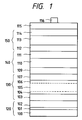
- any imperfection levels and mechanical strain in the vicinity of the interfaces can be decreased and the photovoltaic force and photoelectric currents of the photovoltaic device of the present invention can be increased.
- conductive oxides such as In 2 O 3 , SnO 2 , ITO (In 2 O 3 + SnO 2 ), ZnO, CdO, Cd 2 SnO 4 , TiO 2 , Ta 2 O 5 , Bi 2 O 3 , MoO 3 and Na x WO 3 or a mixture of some of these are preferably used.
- An element capable of changing conductivity i.e., a dopant may also be added to these compounds.
- the power of the RF power source 424 was set to 0.008 W/cm 3 and was applied to the bias rod 428 to cause glow discharge to take place, and the shutter 427 was opened.
- the i-type layer was started to be formed on the RF n-type layer, and an i-type layer with a layer thickness of 10 nm was formed, whereupon the RF glow discharge was stopped and the output from the RF power source 424 was stopped to complete the formation of the RF i-type layer 104.
- Example 1 The procedure of Example 1 was repeated except that the MW i-type semiconductor layer 105 of the third pin structure, comprised of amorphous silicon germanium, was formed using only RF power, SiH 4 gas flow rate, GeH 4 gas flow rate and H 2 gas flow rate were controlled by means of the corresponding mass flow controllers 456, 457 and 458 so as to be 4 sccm, 3 sccm and 200 sccm, respectively, and the pressure inside the i-type layer deposition chamber 418 was controlled so as to be 0.8 Torr, thus, an RF i-type semiconductor layer with a layer thickness of 0.1 ⁇ m was formed.
- SiH 4 gas flow rate, GeH 4 gas flow rate and H 2 gas flow rate were controlled by means of the corresponding mass flow controllers 456, 457 and 458 so as to be 4 sccm, 3 sccm and 200 sccm, respectively, and the pressure inside the i-type layer deposition chamber 418 was controlled so as to be 0.8 Tor
- the photovoltaic device of the present invention is seen to have superior characteristics.
- an MW i-type layer 105 comprised of ⁇ c-SiGe and an RF i-type layer 106 (a buffer layer) comprised of a-Si, both of the third pin structure, were successively formed in the following way.
- the gate valve 408 was opened to carry the substrate 490 (with the above layers formed) into the transport chamber 404 and p-type layer deposition chamber 419 previously evacuated by means of a vacuum exhaust pump (not shown).
- the substrate 490 was heated in the manner the back thereof was brought into close contact with the substrate heater 412.
- the inside of the p-type layer deposition chamber 419 was evacuated by means of the vacuum exhaust pump (not shown) to have a pressure of about 1 ⁇ 10 -5 Torr.
- the gate valve 408 was opened to carry the substrate 490 (with the above layers formed) into the transport chamber 403 previously evacuated by means of a vacuum exhaust pump (not shown), and the gate valve 407 was also opened to carry the substrate 490 into the transport chamber 402 and n-type layer deposition chamber 417 previously evacuated by means of a vacuum exhaust pump (not shown).
- the power of the RF power source 424 was set to 0.15 W/cm 3 , and was applied to the bias rod 428. Thereafter, the power of a microwave power source (0.5 GHz) (not shown) was set to 0.10 W/cm 3 , and the microwave power was fed into the i-type layer deposition chamber 418 through the bias rod 428 to cause glow discharge to take place.
- the i-type layer of the second pin structure was started to be formed on the RF n-type layer of the second pin structure, and a layer with a layer thickness of 1.5 ⁇ m was formed, whereupon the glow discharge was stopped and the output from the bias power source 424 was stopped to complete the formation of the i-type layer 110 of the second pin structure.
- the photovoltaic device of the present invention is seen to have superior characteristics.
- Example 9 the n-type layer 109 of the second pin structure was formed in the same way.
- i-type layer 110 of the second pin structure comprised of ⁇ c-Si, SiH 4 gas flow rate and H 2 gas flow rate were controlled by means of the corresponding mass flow controllers 456 and 458 so as to be 50 sccm and 1,500 sccm, respectively, and B 2 H 6 /H 2 gas flow rate was controlled by means of the mass flow controller 460 so that boron content in microcrystalline silicon of the i-type layer 110 of the second pin structure ranged from 0 ppm to 10.0 ppm, thus photovoltaic devices were produced.
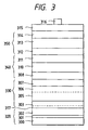
- a photovoltaic device SCEx-16 was produced in which the n-type layer of the third pin structure was changed to have a laminated structure comprised of an amorphous semiconductor layer and a microcrystalline semiconductor layer.
- the constitution is shown in Fig. 3.
- reference numeral 317 denotes an n-type amorphous semiconductor (a-Si) layer and 303 an n-type microcrystalline semiconductor ( ⁇ c-Si) layer.
- a layer 306 was provided as the buffer layer of the i-type layer 305 of the third pin structure.
- the substrate As the substrate, a sheet-like substrate of 300 m long, 30 cm wide and 0.2 mm thick, having light-reflecting layers (a metal layer and a transparent conductive layer) was used. Then, under conditions shown in Table 8 for the other deposited layers, the triple type photovoltaic device was produced in the following way.
- the transparent electrode 115 a mask with a comb-shaped opening was placed, and the comb-shaped collector electrode 116 comprised of Cr(40 nm)/Ag(1,000 nm)/Cr(40 nm) was deposited by vacuum deposition.
- the photovoltaic device of the present invention is seen to have superior characteristics.
- C Unsatisfactory for practical use Boron (B) content in microcrystalline Si (ppm): 0 ppm 1 ppm 3 ppm 8 ppm 10 ppm
Landscapes
- Photovoltaic Devices (AREA)
Applications Claiming Priority (2)
| Application Number | Priority Date | Filing Date | Title |
|---|---|---|---|
| JP226651/96 | 1996-08-28 | ||
| JP22665196 | 1996-08-28 |
Publications (2)
| Publication Number | Publication Date |
|---|---|
| EP0827213A2 true EP0827213A2 (de) | 1998-03-04 |
| EP0827213A3 EP0827213A3 (de) | 1999-05-19 |
Family
ID=16848529
Family Applications (1)
| Application Number | Title | Priority Date | Filing Date |
|---|---|---|---|
| EP97114860A Withdrawn EP0827213A3 (de) | 1996-08-28 | 1997-08-27 | Photovoltaische Vorrichtung |
Country Status (5)
| Country | Link |
|---|---|
| US (1) | US6180870B1 (de) |
| EP (1) | EP0827213A3 (de) |
| KR (1) | KR100251070B1 (de) |
| CN (1) | CN1096714C (de) |
| AU (1) | AU729609B2 (de) |
Cited By (6)
| Publication number | Priority date | Publication date | Assignee | Title |
|---|---|---|---|---|
| EP1032052A1 (de) * | 1999-02-26 | 2000-08-30 | Kaneka Corporation | Herstellungsverfahren für eine auf Silizium basierende Dünnfilmsolarzelle |
| EP1032053A3 (de) * | 1999-02-26 | 2000-09-06 | Kaneka Corporation | Herstellungsverfahren für eine Tandem-Dünnschichtsolarzelle |
| US7064263B2 (en) * | 1998-02-26 | 2006-06-20 | Canon Kabushiki Kaisha | Stacked photovoltaic device |
| US7352044B2 (en) | 2003-01-16 | 2008-04-01 | Tdk Corporation | Photoelectric transducer, photoelectric transducer apparatus, and iron silicide film |
| EP1420461A3 (de) * | 2002-11-13 | 2009-05-06 | Canon Kabushiki Kaisha | Gestapelte photovoltaische Vorrichtung |
| EP2455982A3 (de) * | 2010-11-17 | 2012-11-07 | Samsung SDI Co., Ltd. | Dünnschichtsolarzelle mit einer Polymerstreulichtschicht und Herstellungsverfahren dafür |
Families Citing this family (65)
| Publication number | Priority date | Publication date | Assignee | Title |
|---|---|---|---|---|
| US6303945B1 (en) * | 1998-03-16 | 2001-10-16 | Canon Kabushiki Kaisha | Semiconductor element having microcrystalline semiconductor material |
| JP2001156316A (ja) * | 1999-11-26 | 2001-06-08 | Mitsui High Tec Inc | 太陽電池およびその製造方法 |
| US7122736B2 (en) | 2001-08-16 | 2006-10-17 | Midwest Research Institute | Method and apparatus for fabricating a thin-film solar cell utilizing a hot wire chemical vapor deposition technique |
| JP4162516B2 (ja) * | 2003-03-14 | 2008-10-08 | 三洋電機株式会社 | 光起電力装置 |
| CN100524845C (zh) * | 2003-03-26 | 2009-08-05 | 佳能株式会社 | 叠层型光电元件及其制造方法 |
| JP2004296693A (ja) * | 2003-03-26 | 2004-10-21 | Canon Inc | 積層型光起電力素子および電流バランス調整方法 |
| JP4241446B2 (ja) * | 2003-03-26 | 2009-03-18 | キヤノン株式会社 | 積層型光起電力素子 |
| JP2004356623A (ja) * | 2003-05-08 | 2004-12-16 | Canon Inc | 積層型光起電力素子及びその製造方法 |
| US20060112983A1 (en) * | 2004-11-17 | 2006-06-01 | Nanosys, Inc. | Photoactive devices and components with enhanced efficiency |
| WO2007025062A2 (en) * | 2005-08-25 | 2007-03-01 | Wakonda Technologies, Inc. | Photovoltaic template |
| KR100723137B1 (ko) * | 2005-11-24 | 2007-05-30 | 삼성전기주식회사 | 포토다이오드 소자 및 이를 이용한 광센서용 포토다이오드어레이 |
| US7851695B2 (en) * | 2005-12-26 | 2010-12-14 | Kaneka Corporation | Stacked-type photoelectric conversion device |
| US20070261951A1 (en) * | 2006-04-06 | 2007-11-15 | Yan Ye | Reactive sputtering zinc oxide transparent conductive oxides onto large area substrates |
| US7655542B2 (en) * | 2006-06-23 | 2010-02-02 | Applied Materials, Inc. | Methods and apparatus for depositing a microcrystalline silicon film for photovoltaic device |
| US7674662B2 (en) * | 2006-07-19 | 2010-03-09 | Applied Materials, Inc. | Process for making thin film field effect transistors using zinc oxide |
| SM200600027B (it) * | 2006-08-08 | 2008-02-13 | Stefano Segato | Preparazione fotovoltaica multistrato per la generazione di energia elettrica nonché' metodo di realizzazione ed applicazione |
| FR2910711B1 (fr) * | 2006-12-20 | 2018-06-29 | Centre Nat Rech Scient | Heterojonction a interface intrinsequement amorphe |
| US8747630B2 (en) | 2007-01-16 | 2014-06-10 | Alliance For Sustainable Energy, Llc | Transparent conducting oxides and production thereof |
| US7582515B2 (en) * | 2007-01-18 | 2009-09-01 | Applied Materials, Inc. | Multi-junction solar cells and methods and apparatuses for forming the same |
| US8203071B2 (en) * | 2007-01-18 | 2012-06-19 | Applied Materials, Inc. | Multi-junction solar cells and methods and apparatuses for forming the same |
| US20080223440A1 (en) * | 2007-01-18 | 2008-09-18 | Shuran Sheng | Multi-junction solar cells and methods and apparatuses for forming the same |
| US20080173350A1 (en) * | 2007-01-18 | 2008-07-24 | Applied Materials, Inc. | Multi-junction solar cells and methods and apparatuses for forming the same |
| US20080245414A1 (en) * | 2007-04-09 | 2008-10-09 | Shuran Sheng | Methods for forming a photovoltaic device with low contact resistance |
| US20080254613A1 (en) * | 2007-04-10 | 2008-10-16 | Applied Materials, Inc. | Methods for forming metal interconnect structure for thin film transistor applications |
| US7927713B2 (en) * | 2007-04-27 | 2011-04-19 | Applied Materials, Inc. | Thin film semiconductor material produced through reactive sputtering of zinc target using nitrogen gases |
| US7875486B2 (en) * | 2007-07-10 | 2011-01-25 | Applied Materials, Inc. | Solar cells and methods and apparatuses for forming the same including I-layer and N-layer chamber cleaning |
| WO2009018509A1 (en) * | 2007-08-02 | 2009-02-05 | Applied Materials, Inc. | Thin film transistors using thin film semiconductor materials |
| US20090130827A1 (en) * | 2007-11-02 | 2009-05-21 | Soo Young Choi | Intrinsic amorphous silicon layer |
| WO2009059238A1 (en) * | 2007-11-02 | 2009-05-07 | Applied Materials, Inc. | Plasma treatment between deposition processes |
| US20090114274A1 (en) * | 2007-11-02 | 2009-05-07 | Fritzemeier Leslie G | Crystalline thin-film photovoltaic structures |
| US20090139567A1 (en) * | 2007-11-29 | 2009-06-04 | Philip Chihchau Liu | Conformal protective coating for solar panel |
| US8980066B2 (en) * | 2008-03-14 | 2015-03-17 | Applied Materials, Inc. | Thin film metal oxynitride semiconductors |
| WO2009116990A1 (en) * | 2008-03-17 | 2009-09-24 | Midwest Research Institute | High quality transparent conducting oxide thin films |
| WO2009117438A2 (en) * | 2008-03-20 | 2009-09-24 | Applied Materials, Inc. | Process to make metal oxide thin film transistor array with etch stopping layer |
| US7879698B2 (en) * | 2008-03-24 | 2011-02-01 | Applied Materials, Inc. | Integrated process system and process sequence for production of thin film transistor arrays using doped or compounded metal oxide semiconductor |
| US8258511B2 (en) | 2008-07-02 | 2012-09-04 | Applied Materials, Inc. | Thin film transistors using multiple active channel layers |
| CN101640226B (zh) * | 2008-07-28 | 2012-08-22 | 福建钧石能源有限公司 | 叠层结构和包括该叠层结构的薄膜太阳能电池 |
| EP2330632A1 (de) * | 2008-08-29 | 2011-06-08 | Kaneka Corporation | Fotoelektrischer dünnschichtwandler und herstellungsverfahren dafür |
| US8895842B2 (en) * | 2008-08-29 | 2014-11-25 | Applied Materials, Inc. | High quality TCO-silicon interface contact structure for high efficiency thin film silicon solar cells |
| US8236603B1 (en) | 2008-09-04 | 2012-08-07 | Solexant Corp. | Polycrystalline semiconductor layers and methods for forming the same |
| US20100059110A1 (en) * | 2008-09-11 | 2010-03-11 | Applied Materials, Inc. | Microcrystalline silicon alloys for thin film and wafer based solar applications |
| US20100133094A1 (en) * | 2008-12-02 | 2010-06-03 | Applied Materials, Inc. | Transparent conductive film with high transmittance formed by a reactive sputter deposition |
| US20100163406A1 (en) * | 2008-12-30 | 2010-07-01 | Applied Materials, Inc. | Substrate support in a reactive sputter chamber |
| US8415187B2 (en) * | 2009-01-28 | 2013-04-09 | Solexant Corporation | Large-grain crystalline thin-film structures and devices and methods for forming the same |
| JP4761322B2 (ja) | 2009-04-30 | 2011-08-31 | シャープ株式会社 | 半導体膜の成膜方法および光電変換装置の製造方法 |
| KR101106480B1 (ko) * | 2009-06-12 | 2012-01-20 | 한국철강 주식회사 | 광기전력 장치의 제조 방법 |
| US20110114177A1 (en) * | 2009-07-23 | 2011-05-19 | Applied Materials, Inc. | Mixed silicon phase film for high efficiency thin film silicon solar cells |
| KR101065749B1 (ko) | 2009-07-31 | 2011-09-19 | 주식회사 티지솔라 | 태양전지 및 그 제조방법 |
| KR101733718B1 (ko) | 2009-09-24 | 2017-05-10 | 어플라이드 머티어리얼스, 인코포레이티드 | 소스 및 드레인 금속 식각을 위해 습식 프로세스를 이용하여 금속 산화물 또는 금속 산질화물 tft들을 제조하는 방법들 |
| US8840763B2 (en) * | 2009-09-28 | 2014-09-23 | Applied Materials, Inc. | Methods for stable process in a reactive sputtering process using zinc or doped zinc target |
| WO2011046664A2 (en) * | 2009-10-15 | 2011-04-21 | Applied Materials, Inc. | A barrier layer disposed between a substrate and a transparent conductive oxide layer for thin film silicon solar cells |
| US20110126875A1 (en) * | 2009-12-01 | 2011-06-02 | Hien-Minh Huu Le | Conductive contact layer formed on a transparent conductive layer by a reactive sputter deposition |
| EP2517267A2 (de) * | 2009-12-22 | 2012-10-31 | Oerlikon Solar AG, Trübbach | Tandem-siliziumdünnschicht-solarzelle und verfahren zu ihrer herstellung |
| US20110174362A1 (en) * | 2010-01-18 | 2011-07-21 | Applied Materials, Inc. | Manufacture of thin film solar cells with high conversion efficiency |
| US20110232753A1 (en) * | 2010-03-23 | 2011-09-29 | Applied Materials, Inc. | Methods of forming a thin-film solar energy device |
| CN102244152B (zh) * | 2010-05-12 | 2013-09-04 | 吉林庆达新能源电力股份有限公司 | 一种太阳能电池生产中非晶硅薄膜的沉积方法 |
| KR20120067544A (ko) * | 2010-12-16 | 2012-06-26 | 엘지전자 주식회사 | 박막 태양전지 및 이의 제조 방법 |
| US20130160810A1 (en) * | 2011-12-22 | 2013-06-27 | General Electric Company | Photovoltaic device and method of making |
| WO2013119550A1 (en) | 2012-02-10 | 2013-08-15 | Alliance For Sustainable Energy, Llc | Thin film photovoltaic devices with a minimally conductive buffer layer |
| US20130224899A1 (en) * | 2012-02-28 | 2013-08-29 | International Business Machines Corporation | Enhancing efficiency in solar cells by adjusting deposition power |
| US9214577B2 (en) | 2012-02-28 | 2015-12-15 | International Business Machines Corporation | Reduced light degradation due to low power deposition of buffer layer |
| US9373741B2 (en) * | 2012-08-15 | 2016-06-21 | International Business Machines Corporation | Heterostructure germanium tandem junction solar cell |
| US20150270423A1 (en) | 2012-11-19 | 2015-09-24 | Alliance For Sustainable Energy, Llc | Devices and methods featuring the addition of refractory metals to contact interface layers |
| TW201503390A (zh) * | 2013-07-11 | 2015-01-16 | Univ Nat Cheng Kung | 微晶矽太陽能電池結構及其製造方法 |
| JP6782211B2 (ja) * | 2017-09-08 | 2020-11-11 | 株式会社東芝 | 透明電極、それを用いた素子、および素子の製造方法 |
Citations (2)
| Publication number | Priority date | Publication date | Assignee | Title |
|---|---|---|---|---|
| EP0566972A1 (de) | 1992-04-15 | 1993-10-27 | Canon Kabushiki Kaisha | Photovoltaische Vorrichtung mit einem Pin-Übergang bestehend aus einer i(aSi-Ge)-Schicht mit einem maximalen Punkt für den Ge-Gehalt |
| US5456762A (en) | 1992-12-28 | 1995-10-10 | Canon Kabushiki Kaisha | Photoelectric conversion elements |
Family Cites Families (6)
| Publication number | Priority date | Publication date | Assignee | Title |
|---|---|---|---|---|
| US2949498A (en) | 1955-10-31 | 1960-08-16 | Texas Instruments Inc | Solar energy converter |
| US4490573A (en) * | 1979-12-26 | 1984-12-25 | Sera Solar Corporation | Solar cells |
| DE3854040T2 (de) * | 1987-11-20 | 1995-10-26 | Canon Kk | Photovoltaisches PIN-Bauelement, Tandem-und Triple-Zellen. |
| JP2719230B2 (ja) * | 1990-11-22 | 1998-02-25 | キヤノン株式会社 | 光起電力素子 |
| CA2102948C (en) | 1992-11-16 | 1998-10-27 | Keishi Saito | Photoelectric conversion element and power generation system using the same |
| JP2923193B2 (ja) * | 1993-12-30 | 1999-07-26 | キヤノン株式会社 | 光電変換素子の製造方法 |
-
1997
- 1997-08-27 EP EP97114860A patent/EP0827213A3/de not_active Withdrawn
- 1997-08-27 US US08/917,888 patent/US6180870B1/en not_active Expired - Lifetime
- 1997-08-27 KR KR1019970041383A patent/KR100251070B1/ko not_active Expired - Fee Related
- 1997-08-27 AU AU36048/97A patent/AU729609B2/en not_active Ceased
- 1997-08-28 CN CN97117521A patent/CN1096714C/zh not_active Expired - Fee Related
Patent Citations (2)
| Publication number | Priority date | Publication date | Assignee | Title |
|---|---|---|---|---|
| EP0566972A1 (de) | 1992-04-15 | 1993-10-27 | Canon Kabushiki Kaisha | Photovoltaische Vorrichtung mit einem Pin-Übergang bestehend aus einer i(aSi-Ge)-Schicht mit einem maximalen Punkt für den Ge-Gehalt |
| US5456762A (en) | 1992-12-28 | 1995-10-10 | Canon Kabushiki Kaisha | Photoelectric conversion elements |
Non-Patent Citations (2)
| Title |
|---|
| J. MEIER ET AL., WORLD CONFERENCE ON PHOTOVOLTAIC ENERGY, vol. 1, 1994, pages 409 - 412 |
| PHOTOVOLTAIC SPECIALISTS CONFERENCE, September 1988 (1988-09-01), pages 1469 - 1476 |
Cited By (7)
| Publication number | Priority date | Publication date | Assignee | Title |
|---|---|---|---|---|
| US7064263B2 (en) * | 1998-02-26 | 2006-06-20 | Canon Kabushiki Kaisha | Stacked photovoltaic device |
| EP1032052A1 (de) * | 1999-02-26 | 2000-08-30 | Kaneka Corporation | Herstellungsverfahren für eine auf Silizium basierende Dünnfilmsolarzelle |
| EP1032053A3 (de) * | 1999-02-26 | 2000-09-06 | Kaneka Corporation | Herstellungsverfahren für eine Tandem-Dünnschichtsolarzelle |
| US6190932B1 (en) | 1999-02-26 | 2001-02-20 | Kaneka Corporation | Method of manufacturing tandem type thin film photoelectric conversion device |
| EP1420461A3 (de) * | 2002-11-13 | 2009-05-06 | Canon Kabushiki Kaisha | Gestapelte photovoltaische Vorrichtung |
| US7352044B2 (en) | 2003-01-16 | 2008-04-01 | Tdk Corporation | Photoelectric transducer, photoelectric transducer apparatus, and iron silicide film |
| EP2455982A3 (de) * | 2010-11-17 | 2012-11-07 | Samsung SDI Co., Ltd. | Dünnschichtsolarzelle mit einer Polymerstreulichtschicht und Herstellungsverfahren dafür |
Also Published As
| Publication number | Publication date |
|---|---|
| KR100251070B1 (ko) | 2000-04-15 |
| CN1096714C (zh) | 2002-12-18 |
| AU3604897A (en) | 1998-03-05 |
| EP0827213A3 (de) | 1999-05-19 |
| AU729609B2 (en) | 2001-02-08 |
| US6180870B1 (en) | 2001-01-30 |
| KR19980019054A (ko) | 1998-06-05 |
| CN1175095A (zh) | 1998-03-04 |
Similar Documents
| Publication | Publication Date | Title |
|---|---|---|
| US6180870B1 (en) | Photovoltaic device | |
| US6835888B2 (en) | Stacked photovoltaic device | |
| US6166319A (en) | Multi-junction photovoltaic device with microcrystalline I-layer | |
| US5913986A (en) | Photovoltaic element having a specific doped layer | |
| US5720826A (en) | Photovoltaic element and fabrication process thereof | |
| US5279679A (en) | Multi-layered photovoltaic element having at least three unit cells | |
| EP1271661B1 (de) | Photovoltaische Vorrichtung | |
| US6399411B1 (en) | Method for forming non-single-crystal semiconductor thin film, and method for producing photovoltaic device | |
| US6911594B2 (en) | Photovoltaic device | |
| JP2004165394A (ja) | 積層型光起電力素子 | |
| US6495392B2 (en) | Process for producing a semiconductor device | |
| JP3684041B2 (ja) | 光起電力素子 | |
| JPH11261102A (ja) | 光起電力素子 | |
| JPH11261087A (ja) | 光起電力素子 | |
| JPH11103082A (ja) | 光起電力素子及びその作製方法 | |
| JP2895213B2 (ja) | 光起電力素子 | |
| JP3659511B2 (ja) | 光起電力素子 | |
| JP2007189266A (ja) | 積層型光起電力素子 | |
| AU756834B2 (en) | Method of producing a microcrystal semiconductor thin film | |
| JPH10229209A (ja) | 光起電力素子 | |
| JPH09191119A (ja) | 光起電力素子の製造方法 | |
| JPH04255273A (ja) | 光起電力素子 |
Legal Events
| Date | Code | Title | Description |
|---|---|---|---|
| PUAI | Public reference made under article 153(3) epc to a published international application that has entered the european phase |
Free format text: ORIGINAL CODE: 0009012 |
|
| AK | Designated contracting states |
Kind code of ref document: A2 Designated state(s): CH DE IT LI |
|
| PUAL | Search report despatched |
Free format text: ORIGINAL CODE: 0009013 |
|
| AK | Designated contracting states |
Kind code of ref document: A3 Designated state(s): AT BE CH DE DK ES FI FR GB GR IE IT LI LU MC NL PT SE |
|
| 17P | Request for examination filed |
Effective date: 19991005 |
|
| AKX | Designation fees paid |
Free format text: CH DE IT LI |
|
| 17Q | First examination report despatched |
Effective date: 20071009 |
|
| STAA | Information on the status of an ep patent application or granted ep patent |
Free format text: STATUS: THE APPLICATION HAS BEEN WITHDRAWN |
|
| 18W | Application withdrawn |
Effective date: 20091118 |