EP0827286A2 - Telekommunikationsgerät mit als Ringschaltung ausgeführter Schaltvorrichtung - Google Patents
Telekommunikationsgerät mit als Ringschaltung ausgeführter Schaltvorrichtung Download PDFInfo
- Publication number
- EP0827286A2 EP0827286A2 EP97202554A EP97202554A EP0827286A2 EP 0827286 A2 EP0827286 A2 EP 0827286A2 EP 97202554 A EP97202554 A EP 97202554A EP 97202554 A EP97202554 A EP 97202554A EP 0827286 A2 EP0827286 A2 EP 0827286A2
- Authority
- EP
- European Patent Office
- Prior art keywords
- switching
- switching elements
- branches
- compensation
- parallel
- Prior art date
- Legal status (The legal status is an assumption and is not a legal conclusion. Google has not performed a legal analysis and makes no representation as to the accuracy of the status listed.)
- Withdrawn
Links
Images
Classifications
-
- H—ELECTRICITY
- H04—ELECTRIC COMMUNICATION TECHNIQUE
- H04B—TRANSMISSION
- H04B1/00—Details of transmission systems, not covered by a single one of groups H04B3/00 - H04B13/00; Details of transmission systems not characterised by the medium used for transmission
- H04B1/38—Transceivers, i.e. devices in which transmitter and receiver form a structural unit and in which at least one part is used for functions of transmitting and receiving
- H04B1/40—Circuits
- H04B1/44—Transmit/receive switching
- H04B1/48—Transmit/receive switching in circuits for connecting transmitter and receiver to a common transmission path, e.g. by energy of transmitter
Definitions
- the invention relates to a telecommunications device, in particular a Radio, with a switching device designed as a ring circuit, the four Has switching branches, each with a switching element, for optional Coupling of two first signal paths with two second signal paths serves and whose switching elements compensation branches are connected in parallel, each for Generation of a parallel resonance together with a blocking switching element to serve.
- a radio is known, the one as a ring circuit executed switching device with four switching branches contains.
- the switching branches each contain a switching element and are used to couple the transmitter or the Receiver of the radio with one of two transmit / receive antennas each.
- a Switching element of the switching device may in particular be in the blocking state Do not let high-frequency signals through or only let insignificant portions through.
- each switching element has a compensation branch in parallel switch that with an execution of the switching elements as a semiconductor switch parallel switching element in its locked state has a parallel resonance causes.
- This increases the blocking effect of a semiconductor switch in the open (locking) condition.
- the blocking effect of an open semiconductor switch is affected by the fact that in the blocking state to the outside essentially capacity due to housing influences is effective, which leads to a reduced Attenuation or partial transmission of high-frequency signals leads. This is for all radio applications relevant, e.g. B. with GSM devices ("Global System for Mobile communications ") or DECT devices (" Digital European Cordless Telecommunication ").
- the compensation branches connected in parallel are used for compensation of this effect.
- the invention is based, the telecommunications device to change the type mentioned in such a way that the number of to realize the Switching device of the telecommunications device required components is reduced.
- the object is achieved in that the assignment of a compensation branch to one of the switching elements depends on the switching state of the switching device.
- two compensation branches are provided, one of which is two opposite connections of the switching device and the other the two connects other connections, being in the different switching states
- Switching device only one of the semiconductor switching elements Switching elements are in the on state and in the compensation branches
- Inductors are arranged to generate parallel resonances with the externally effective capacity of the blocking switching elements, which is in the Passing state switching element are adjacent, serve.
- the semiconductor switching elements are designed as switching diodes by applying suitable DC voltages in their on state or in have their locking status transferred.
- the invention also relates to a switching device with four in a ring circuit arranged switching branches, each with a switching element, in which the Switching elements compensation branches are connected in parallel, each for Generation of a parallel resonance together with a blocking switching element serve, and in which the assignment of a compensation branch to one of the Switching elements is dependent on the switching state of the switching device.
- the Switching device can be used universally in all devices where four Signal paths for AC or radio frequency signals must be switched and, as already mentioned, leads to a reduction in the realization of Compensation means required for the switching elements used Components.
- a transmitter and a receiver are optional two antennas coupled, e.g. in mobile terminals in motor vehicles be used, is used. For this application there is one Switching from the transmitting / receiving antenna of the mobile radio terminal to one Transmitting / receiving external antenna of the motor vehicle advantageous.
- the invention relates also relates to a method for operating such a switching device.
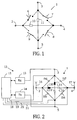
- the switching device 1 shown in FIG. 1 and designed as a ring circuit has connections 2, 3, 4 and 5, which are for coupling with different Signal paths are provided. Controllable are between the connections 2 to 5 Switching elements 6, 7, 8 and 9, the controllability of which is indicated by arrows.
- connection 3 Between the connections 2 and 3 is the switching element 6, between the Connections 3 and 4, the switching element 7, between the connections 4 and 5 that Switching element 8 and between the connections 5 and 2, the switching element 9.
- Two Opposing connections can optionally be made by appropriate Control of the switching elements 6 to 9 with a different one of the two Couple other connections. So the connection 3 with the connections 2 and 4 and port 5 also connect to ports 2 and 4.
- only switching states are provided in which one of the four switching elements is in the on state and the remaining three Switching elements are in the blocking state. For example, if Switching element 6 switched to its on state, the rest Switching elements 7 to 9 set in their blocking state. In this switching state can either a signal from port 2 to port 3 or vice versa Signal from port 3 to port 2 are transmitted.
- An impedance 10 is connected between the terminals 2 and 4, so that parallel to the switching elements 6 and 7 or parallel to the switching elements 8 and 9 lies. Between the connections 3 and 5 there is an impedance 11, which is thus parallel to the switching elements 6 and 9 or parallel to the switching elements 7 and 8 lies.
- the branches with the impedances 10 and 11 form two compensation branches, to compensate for the switching elements 6 in the blocking state to 9 externally effective capacities of the switching elements 6 to 9 serve.
- semiconductor switching elements have a corresponding one in the blocking state parasitic capacitance, which is essentially due to the housing capacity such components is determined. So that the switching elements 6 to 9 for AC and especially high-frequency signals also in the blocking state partially permeable.
- the impedances 10 and 11 are now designed to match the neighboring ones blocking switching elements of a switching element in the on state one parallel resonance circuit each for a narrow band Form frequency range. This causes an increased damping through the blocking (i.e. open) switching elements. For example form the switching element 6 in the on state (i.e. in the closed state) on the one hand the impedance 11 with the switching element 9 via the switching element 6 and on the other hand, the impedance 10 with the switching element 7 via the switching element 6 one parallel resonance circuit each. Depending on the frequency, the values are the To design impedances 10 and 11 for generating parallel resonances.
- switching element 6 in the on state are accordingly the impedances 10 and 11 the switching element 7 and the switching element 9 for generating a Assigned parallel resonance.
- switching element 6 to 9 are in the on state and the rest Switching elements are controlled in their blocking state changes the assignment of the compensation branches according to the specified circuit diagram with the impedances 10 so that they each the two adjacent switching elements of the switching element in the on state for generating Parallel resonances are assigned.
- the radio 12 is, for example, a mobile radio terminal according to the GSM standard or a cordless telephone according to the DECT standard. However, the invention is not limited to such radio devices. Also one Application in other telecommunication devices in which two transmit / or Receive signals are each assigned to one of two possible signal paths, comes into consideration for the invention.
- the present radio 12 contains one Receiver 13 and a transmitter 14, both coupled to a digital part 15 are to implement digital signal processing from the receiver 13 received signals or signals emitted via the transmitter 14 is. 15 microprocessors and / or signal processors are usually used in the digital part used. The receiver 13 is still connected to the connector 3 Switching device 1 coupled.
- the transmitter 14 is correspondingly connected to the connector 5 the switching device 1 coupled.
- the connections 2 and 4 of the switching device 1 are each coupled to an antenna.
- At the connection 2 is a transmit / receive antenna 16
- at the connection 4 is a transmit / receive antenna 17th connected.
- the switching elements 6 to 9 of the Switching device 1 are in this embodiment as switching diodes D6, D7, D8 and D9 realized. Another implementation would be a realization, for example of the switching elements 6 to 9 by transistor switching elements.
- the impedance is 10 through a series connection of an inductor L10 and a capacitor C10 realized.
- the impedance 11 is a series connection of an inductance L11 and a capacitor C11 realized.
- the inductors L10 and L11 are used for Generation of parallel resonances together with the depending on the switching state Switching device 1 associated blocking two switching diodes.
- the Generation of parallel resonances and their purpose is already related has been described with Fig. 1. In the present case, a partial transmission of signals generated by transmitter 14 with high power suppressed to the receiver 13, causing malfunction or destruction of the receiver 13 can be avoided.
- the switching diodes D6 to D9 are controlled by control lines 18 to 21 transmitted DC signals. By suitable selection of DC voltage values the diodes D6 to D9 are in their conductive or blocking state transferred.
- the capacitors C10 and C11 are used for DC decoupling of the two connections of the compensation branch with the impedance 10 or two connections of the compensation branch with impedance 11, which is because of Control of the switching diodes D6 to D9 with the aid of direct current signals is required.
Landscapes
- Engineering & Computer Science (AREA)
- Computer Networks & Wireless Communication (AREA)
- Signal Processing (AREA)
- Transceivers (AREA)
- Input Circuits Of Receivers And Coupling Of Receivers And Audio Equipment (AREA)
- Waveguide Switches, Polarizers, And Phase Shifters (AREA)
- Electronic Switches (AREA)
- Variable-Direction Aerials And Aerial Arrays (AREA)
Abstract
Description
Claims (6)
- Telekommunikationsgerät, insbesondere Funkgerät, mit einer als Ringschaltung ausgeführten Schaltvorrichtung (1), die vier Schaltzweige mit jeweils einem Schaltelement (6, ... , 9; D6, ... , D9) aufweist, die zur wahlweisen Kopplung von zwei ersten Signalwegen (3, 5) mit zwei zweiten Signalwegen (2, 4) dient und deren Schaltelementen (6, ... , 9; D6, ... , D9) Kompensationszweige (10,11; L10, C10, L11, C11) parallel geschaltet sind, die jeweils zur Erzeugung einer Parallelresonanz zusammen mit einem sperrenden Schaltelement dienen,
dadurch gekennzeichnet,daß die Zuordnung eines Kompensationszweiges (10,11; L10, C10, L11, C11) zu einem der Schaltelemente (6, ... , 9; D6, ... , D9) vom Schaltzustand der Schaltvorrichtung (1) abhängig ist. - Telekommunikationsgerät nach Anspruch 1,
dadurch gekennzeichnet,daß zwei Kompensationszweige (10,11; L10, C10, L11, C11) vorgesehen sind, von denen einer (10; L10, C10) zwei gegenüberliegende Anschlüsse (2, 4) der Schaltvorrichtung und der andere (11; L11, C11) die beiden anderen Anschlüsse (3, 5) verbindet,daß in den verschiedenen Schaltzuständen der Schaltvorrichtung (1) sich nur eines der aus Halbleiterschaltelementen (D6, ..., D9) bestehenden Schaltelemente (6, ..., 9) im Durchlaßzustand befindet unddaß in den Kompensationszweigen Induktivitäten (L10, L11) angeordnet sind, die zur Erzeugung von Parallelresonanzen mit der nach außen wirksamen Kapazität der sperrenden Schaltelemente, die dem sich im Durchlaßzustand befindenden Schaltelement benachbart sind, dienen. - Telekommunikationsgerät nach Anspruch 2,
dadurch gekennzeichnet,daß Schaltdioden (D6, ..., D9) als Schaltelemente (6, ..., 9) dienen. - Telekommunikationsgerät nach einem der Ansprüche 1 bis 3,
dadurch gekennzeichnet,daß den zwei ersten Signalwegen (3, 5) ein Empfänger (13) und ein Sender (14) zugeordnet sind unddaß den zwei zweiten Signalwegen (2, 4) jeweils eine Antenne (2, 4) zugeordnet ist. - Schaltvorrichtung (1) mit vier in einer Ringschaltung angeordneten Schaltzweigen mit jeweils einem Schaltelement (6, ... , 9; D6, ... , D9), bei der den Schaltelementen Kompensationszweige (10,11; L10, C10, L11, C11) parallel geschaltet sind, die jeweils zur Erzeugung einer Parallelresonanz zusammen mit einem sperrenden Schaltelement dienen,
dadurch gekennzeichnet,daß die Zuordnung eines Kompensationszweiges (10,11; L10, C10, L11, C11) zu einem der Schaltelemente (6, ... , 9; D6, ... , D9) vom Schaltzustand der Schaltvorrichtung (1) abhängig ist. - Verfahren zum Betreiben einer Schaltvorrichtung (1) mit vier in einer Ringschaltung angeordneten Schaltzweigen mit jeweils einem Schaltelement (6, ... , 9; D6, ... , D9), bei der den Schaltelementen Kompensationszweige (10,11; L10, C10, L11, C11) parallel geschaltet sind, die jeweils zur Erzeugung einer Parallelresonanz zusammen mit einem sperrenden Schaltelement dienen,
dadurch gekennzeichnet,daß die Zuordnung eines Kompensationszweiges (10,11; L10, C10, L11, C11) zu einem der Schaltelemente (6, ... , 9; D6, ... , D9) in Abhängigkeit von die Schaltelemente steuernden Steuersignalen (18, 19, 20, 21) festgelegt wird.
Applications Claiming Priority (2)
| Application Number | Priority Date | Filing Date | Title |
|---|---|---|---|
| DE19635175A DE19635175A1 (de) | 1996-08-29 | 1996-08-29 | Telekommunikationsgerät mit als Ringschaltung ausgeführter Schaltvorrichtung |
| DE19635175 | 1996-08-29 |
Publications (2)
| Publication Number | Publication Date |
|---|---|
| EP0827286A2 true EP0827286A2 (de) | 1998-03-04 |
| EP0827286A3 EP0827286A3 (de) | 2003-05-21 |
Family
ID=7804170
Family Applications (1)
| Application Number | Title | Priority Date | Filing Date |
|---|---|---|---|
| EP97202554A Withdrawn EP0827286A3 (de) | 1996-08-29 | 1997-08-20 | Telekommunikationsgerät mit als Ringschaltung ausgeführter Schaltvorrichtung |
Country Status (4)
| Country | Link |
|---|---|
| US (1) | US5991607A (de) |
| EP (1) | EP0827286A3 (de) |
| JP (1) | JPH1098410A (de) |
| DE (1) | DE19635175A1 (de) |
Families Citing this family (9)
| Publication number | Priority date | Publication date | Assignee | Title |
|---|---|---|---|---|
| WO2000041326A1 (en) * | 1999-01-07 | 2000-07-13 | Motorola Inc. | A radio frequency (rf) switch using a single quarter wave isolating section and method of forming same |
| US6806791B1 (en) * | 2000-02-29 | 2004-10-19 | Radio Frequency Systems, Inc. | Tunable microwave multiplexer |
| JP2004048220A (ja) * | 2002-07-10 | 2004-02-12 | Alps Electric Co Ltd | 送受切替回路 |
| US7719383B2 (en) * | 2007-04-30 | 2010-05-18 | Zeji Gu | High isolation electronic multiple pole multiple throw switch |
| US7816996B2 (en) * | 2007-12-18 | 2010-10-19 | Zeji Gu | Non-reflective MPNT switch |
| US9136838B2 (en) * | 2010-09-21 | 2015-09-15 | Dsp Group Ltd. | RF switch implementation in CMOS process |
| US20130252562A1 (en) * | 2010-09-21 | 2013-09-26 | Dsp Group, Ltd. | High power high isolation low current cmos rf switch |
| US9735854B2 (en) * | 2016-01-18 | 2017-08-15 | Qorvo Us, Inc. | Systems for antenna swapping switching and methods of operation thereof |
| US9793972B1 (en) | 2016-04-04 | 2017-10-17 | Qorvo Us, Inc. | Multiple-input multiple-output (MIMO) antenna swapping circuit |
Family Cites Families (6)
| Publication number | Priority date | Publication date | Assignee | Title |
|---|---|---|---|---|
| DE4430987C1 (de) * | 1994-08-31 | 1995-11-23 | Siemens Ag | Antennenschalter für drahtlose Antennendiversity-Telekommunikationsgeräte mit zwei Antennen |
| JP3163918B2 (ja) * | 1994-11-28 | 2001-05-08 | 株式会社村田製作所 | 高周波スイッチ |
| JPH08204530A (ja) * | 1995-01-23 | 1996-08-09 | Sony Corp | スイツチ回路 |
| US5625894A (en) * | 1995-03-21 | 1997-04-29 | Industrial Technology Research Institute | Switch filter having selectively interconnected filter stages and ports |
| US5584053A (en) * | 1995-08-04 | 1996-12-10 | Motorola, Inc. | Commonly coupled high frequency transmitting/receiving switching module |
| JP3332194B2 (ja) * | 1995-08-10 | 2002-10-07 | ソニー株式会社 | スイツチ半導体集積回路及び通信端末装置 |
-
1996
- 1996-08-29 DE DE19635175A patent/DE19635175A1/de not_active Withdrawn
-
1997
- 1997-08-20 EP EP97202554A patent/EP0827286A3/de not_active Withdrawn
- 1997-08-27 US US08/918,968 patent/US5991607A/en not_active Expired - Fee Related
- 1997-08-29 JP JP9233591A patent/JPH1098410A/ja active Pending
Also Published As
| Publication number | Publication date |
|---|---|
| EP0827286A3 (de) | 2003-05-21 |
| DE19635175A1 (de) | 1998-03-05 |
| JPH1098410A (ja) | 1998-04-14 |
| US5991607A (en) | 1999-11-23 |
Similar Documents
| Publication | Publication Date | Title |
|---|---|---|
| DE69615914T2 (de) | Funkübertragungsvorrichtung für Zeitmultiplex-Vielfachzugriffssystem | |
| DE69835937T2 (de) | Zweifrequenzschalter, anordnung mit gemeinsamer zweifrequenzantenne und mobile zweifrequenz-funkübertragungsausrüstung damit | |
| DE69517348T2 (de) | Anordnung zur Trennung von Sende- und Empfangssignalen in einem Sende-Empfangsgerät | |
| DE19823060C2 (de) | Leistungsverstärker-Ausgangsschaltung | |
| DE69834679T2 (de) | Antennenweiche | |
| DE69221355T2 (de) | Scheibenantennensystem für Kraftfahrzeug | |
| DE69513719T2 (de) | Duplexer | |
| DE68907613T2 (de) | Anordnung mit bandsperrfiltern. | |
| DE102008049063B4 (de) | Hochfrequenz-Vorstufe und Empfänger | |
| DE19853484A1 (de) | Hochfrequente Schalteinrichtung | |
| DE10105942A1 (de) | Einpoliger Umschalter und Kommunikationseinheit unter Verwendung desselben | |
| EP1352482A2 (de) | Elektrisches schaltmodul, schaltmodulanordnung und verwendung des schaltmoduls und der schaltmodulanordnung | |
| EP1168500A2 (de) | Antennenumschalter für Sende-Empfangseinheiten in einer Mobilstation | |
| EP0827286A2 (de) | Telekommunikationsgerät mit als Ringschaltung ausgeführter Schaltvorrichtung | |
| EP1119918B1 (de) | Sendeendstufe für ein mobiltelefon | |
| DE3203961C2 (de) | ||
| DE19810620B4 (de) | Breitbanddämpfungseinrichtung zur frequenzkompensierten Dämpfung von Hochfrequenzsignalen eines Frequenzbandes | |
| DE10305379A1 (de) | Frontendschaltung | |
| EP0850512B1 (de) | Funkgerät mit mehreren frequenzbereichen | |
| DE102019101888B4 (de) | Konfigurierbares mikroakustisches HF-Filter | |
| DE3108993C2 (de) | HF-Eingangsfilterschaltung eines Tuners | |
| DE102005020084B4 (de) | Empfänger mit Hochfrequenz-Schaltanordnung | |
| DE19948964C2 (de) | Schaltungsanordnung zum Herstellen einer unidirektionalen Verbindung zwischen Sende- und/oder Empfangsgeräten und einer Antenne | |
| DE2927225A1 (de) | Schaltung zum mischen und frequenzband-umschalten fuer ein mehrband-abstimmsystem | |
| DE1924680B2 (de) | Transistor-mischschaltung |
Legal Events
| Date | Code | Title | Description |
|---|---|---|---|
| PUAI | Public reference made under article 153(3) epc to a published international application that has entered the european phase |
Free format text: ORIGINAL CODE: 0009012 |
|
| AK | Designated contracting states |
Kind code of ref document: A2 Designated state(s): AT BE CH DE DK ES FI FR GB GR IE IT LI LU MC NL PT SE |
|
| RAP3 | Party data changed (applicant data changed or rights of an application transferred) |
Owner name: KONINKLIJKE PHILIPS ELECTRONICS N.V. Owner name: PHILIPS PATENTVERWALTUNG GMBH |
|
| RAP3 | Party data changed (applicant data changed or rights of an application transferred) |
Owner name: KONINKLIJKE PHILIPS ELECTRONICS N.V. Owner name: PHILIPS CORPORATE INTELLECTUAL PROPERTY GMBH |
|
| RAP1 | Party data changed (applicant data changed or rights of an application transferred) |
Owner name: KONINKLIJKE PHILIPS ELECTRONICS N.V. Owner name: PHILIPS CORPORATE INTELLECTUAL PROPERTY GMBH |
|
| PUAL | Search report despatched |
Free format text: ORIGINAL CODE: 0009013 |
|
| RAP1 | Party data changed (applicant data changed or rights of an application transferred) |
Owner name: KONINKLIJKE PHILIPS ELECTRONICS N.V. Owner name: PHILIPS INTELLECTUAL PROPERTY & STANDARDS GMBH |
|
| AK | Designated contracting states |
Designated state(s): AT BE CH DE DK ES FI FR GB GR IE IT LI LU MC NL PT SE |
|
| RIC1 | Information provided on ipc code assigned before grant |
Ipc: 7H 03K 17/76 B Ipc: 7H 04B 1/48 A |
|
| 17P | Request for examination filed |
Effective date: 20031121 |
|
| AKX | Designation fees paid |
Designated state(s): DE FR GB |
|
| 17Q | First examination report despatched |
Effective date: 20041228 |
|
| STAA | Information on the status of an ep patent application or granted ep patent |
Free format text: STATUS: THE APPLICATION IS DEEMED TO BE WITHDRAWN |
|
| 18D | Application deemed to be withdrawn |
Effective date: 20050510 |