EP0828247B1 - Equipement de transmission de données et méthode associée - Google Patents
Equipement de transmission de données et méthode associée Download PDFInfo
- Publication number
- EP0828247B1 EP0828247B1 EP97115346A EP97115346A EP0828247B1 EP 0828247 B1 EP0828247 B1 EP 0828247B1 EP 97115346 A EP97115346 A EP 97115346A EP 97115346 A EP97115346 A EP 97115346A EP 0828247 B1 EP0828247 B1 EP 0828247B1
- Authority
- EP
- European Patent Office
- Prior art keywords
- data
- main
- modulating
- level
- subordinate
- Prior art date
- Legal status (The legal status is an assumption and is not a legal conclusion. Google has not performed a legal analysis and makes no representation as to the accuracy of the status listed.)
- Expired - Lifetime
Links
Images


Classifications
-
- H—ELECTRICITY
- H04—ELECTRIC COMMUNICATION TECHNIQUE
- H04L—TRANSMISSION OF DIGITAL INFORMATION, e.g. TELEGRAPHIC COMMUNICATION
- H04L25/00—Baseband systems
- H04L25/38—Synchronous or start-stop systems, e.g. for Baudot code
- H04L25/40—Transmitting circuits; Receiving circuits
- H04L25/49—Transmitting circuits; Receiving circuits using code conversion at the transmitter; using predistortion; using insertion of idle bits for obtaining a desired frequency spectrum; using three or more amplitude levels ; Baseband coding techniques specific to data transmission systems
- H04L25/4906—Transmitting circuits; Receiving circuits using code conversion at the transmitter; using predistortion; using insertion of idle bits for obtaining a desired frequency spectrum; using three or more amplitude levels ; Baseband coding techniques specific to data transmission systems using binary codes
-
- G—PHYSICS
- G11—INFORMATION STORAGE
- G11B—INFORMATION STORAGE BASED ON RELATIVE MOVEMENT BETWEEN RECORD CARRIER AND TRANSDUCER
- G11B20/00—Signal processing not specific to the method of recording or reproducing; Circuits therefor
- G11B20/10—Digital recording or reproducing
- G11B20/14—Digital recording or reproducing using self-clocking codes
- G11B20/1403—Digital recording or reproducing using self-clocking codes characterised by the use of two levels
- G11B20/1423—Code representation depending on subsequent bits, e.g. delay modulation, double density code, Miller code
- G11B20/1426—Code representation depending on subsequent bits, e.g. delay modulation, double density code, Miller code conversion to or from block codes or representations thereof
-
- H—ELECTRICITY
- H04—ELECTRIC COMMUNICATION TECHNIQUE
- H04L—TRANSMISSION OF DIGITAL INFORMATION, e.g. TELEGRAPHIC COMMUNICATION
- H04L12/00—Data switching networks
- H04L12/50—Circuit switching systems, i.e. systems in which the path is physically permanent during the communication
- H04L12/52—Circuit switching systems, i.e. systems in which the path is physically permanent during the communication using time division techniques
-
- H—ELECTRICITY
- H04—ELECTRIC COMMUNICATION TECHNIQUE
- H04L—TRANSMISSION OF DIGITAL INFORMATION, e.g. TELEGRAPHIC COMMUNICATION
- H04L25/00—Baseband systems
- H04L25/02—Details ; arrangements for supplying electrical power along data transmission lines
- H04L25/03—Shaping networks in transmitter or receiver, e.g. adaptive shaping networks
- H04L25/03828—Arrangements for spectral shaping; Arrangements for providing signals with specified spectral properties
- H04L25/03866—Arrangements for spectral shaping; Arrangements for providing signals with specified spectral properties using scrambling
-
- G—PHYSICS
- G11—INFORMATION STORAGE
- G11B—INFORMATION STORAGE BASED ON RELATIVE MOVEMENT BETWEEN RECORD CARRIER AND TRANSDUCER
- G11B2220/00—Record carriers by type
- G11B2220/20—Disc-shaped record carriers
- G11B2220/25—Disc-shaped record carriers characterised in that the disc is based on a specific recording technology
- G11B2220/2537—Optical discs
-
- H—ELECTRICITY
- H04—ELECTRIC COMMUNICATION TECHNIQUE
- H04L—TRANSMISSION OF DIGITAL INFORMATION, e.g. TELEGRAPHIC COMMUNICATION
- H04L1/00—Arrangements for detecting or preventing errors in the information received
- H04L1/004—Arrangements for detecting or preventing errors in the information received by using forward error control
- H04L1/0056—Systems characterized by the type of code used
- H04L1/0064—Concatenated codes
- H04L1/0065—Serial concatenated codes
Definitions
- the present invention relates to an equipment for transmitting data and a method of the same, which can be applied, for example, to an optical disc drive.
- the equipment and the method according to the invention when compensating a dc level of a modulating data, main and subordinate modulated data to be used for recording are provided in the time division and the dc level is calculated in advance, and the modulating data is generated on the basis of the calculation result.
- the total construction can be simplified and the circuit blocks for the transmission system can be used commonly to different systems.
- a method and apparatus for recording data on recording medium is revealed in document EP 0 660 325 A1.
- the data is divided into parts each having a certain constant length so as to prevent the DC component from building up.
- a resynchronization signal RESYNC is inserted in the break between the parts, the data is preliminarily modulated and encoded subsequent to the RESYNC, the DC component thereof is counted, and the pattern of the RESYNC is changed in the direction so that the phase becomes a minus value when the sum of the DC component DSV (digital sum value) up to before that RESYNC is a plus value and becomes a plus value when the sum is a minus value, that is the DSV converges to zero, and the changed data is subjected to modulation and encoding, thereby to reduce the DC component of the recording data.
- DSV digital sum value
- a dc level of a modulating data is calculated in advance, and on the basis of the calculation, the dc level of the modulating data is compensated; and thereby, the dc level of the modulating data can be suppressed and a recorded data can reliably be reproduced.
- Fig. 7 is a block diagram showing a part of the optical disc drive disclosed in the Japanese Patent Application Laid Open no. 6-162668.
- a modulation circuit 2 modulates a data D1 to be used for recording in accordance with the modulation system suitable for the recording characteristic of an optical disc and outputs.
- a pattern generator 3 receives an output data D2 from the modulation circuit 2, and when the output data D2 is the logic "1", the pattern generator 3 inverts the logical level and outputs.
- An up-down counter 4 receives an output data D3 from the pattern generator 3, and when the output data D3 is the logic "1", the up-down counter 4 counts up the count value in each one frame of the output data D3, and when the output data D3 is the logic "0", the up-down counter 4 counts down the count value. Thereby, the up-down counter 4 detects the dc level of the output data D3 in each one frame.
- a sign inverter 5 receives the count value from the up-down counter 4, and inverts the sign of the count value and outputs. Thereby, the sign inverter 5 detects the dc level of the output data D3 when the sign of the output data D2 is inverted.
- An adder 6A outputs the addition of the count value from the up-down counter 4 and an accumulated value stored in an accumulated value memory 7.
- An adder 6B outputs the addition of the output value from the sign inverter 5 and the accumulated value stored in the accumulated value memory 7.
- the accumulated value memory 7 is designed to hold an accumulated value of a dc level of continuous modulating data.
- An absolute value comparator 8 makes an added value by the adder 6A and an added value by the adder 6B into an absolute value of the former and an absolute value of the latter, respectively, and thereafter outputs the comparison result.
- a selector 9 selects the added value by the adder 6A or the added value by the adder 6B on the basis of the comparison result, and stores the selected added value in the accumulated value memory 7. Thereby, the selector 9 selects the added value by the adder 6A or the added value by the adder 6B so as to decrease the accumulated value of the dc level.
- a one block shift register 11 delays the data D1 to be used for recording for the period of one frame and outputs the data.
- a modulation circuit 12 modulates the data D1 into the output data D2 in accordance with the same modulation system as the modulation circuit 2.
- a synchronization pattern switching circuit 13 switches the polarity of the output data D2 from a synchronizing signal added to the output data D2 on the basis of the comparison result of the absolute value comparator 8 and outputs the data.
- the synchronization pattern switching circuit 13 switches the polarity of the output data D2 so as to correspond with the selecting process by the selector 9.
- a pattern generator 14 processing the input data in the same manner as the pattern generator 3, inverts the logic of the output data, when the output data from the synchronizing signal pattern switching circuit 13 is the logic "1". Thereby, in the optical disc drive 1, the dc level of the output data D3 is detected by the up-down counter 4 in advance for one frame to the output data D3 from the pattern generator 14, and on the basis of this detection result, the pattern of the synchronizing signal is switched so as to reduce the dc level.
- the data D1 to be used for recording is designed to be delayed for the period of one frame by the one block shift register 11.
- the circuit scale of the one block shift register 11 made of delay circuits is apt to become large, and thereby the total construction becomes large to that extent, which is a problem.
- the present invention has been made in view of the foregoing problems, and an object of the present invention is to provide an equipment for transmitting data and a method of the same, whereby the total construction can be simplified and circuit blocks for the transmission system can commonly be used in different systems.
- the invention is provided with storage means for outputting in the time division a main modulated data and a subordinate modulated data precedent to the main modulated data, and dc level compensation means for compensating a dc level of a main modulating data generated from the main modulated data on the basis of a dc level of a modulating data detected from the subordinate modulated data.
- the storage means output in the time division the main modulated data and the subordinate modulated data, the dc level of the modulating data can be detected in advance from the subordinate modulated data without delay circuits provided, and on the basis of the dc level detected in advance, the dc level of the following main modulated data can be compensated.
- Fig. 2 is a block diagram showing an optical disc drive relating to one embodiment of the present invention.
- This optical disc drive 20 applied to an external storage for a computer or the like, records a user data D5 in a magneto-optic disc 21, and reproduces and outputs the user data D5 recorded in the magneto-optic disc 21.
- the magneto-optic disc 21 is provided with the track address and the sector address formatted in advance by the pregroove forming the guide groove for laser beams.
- an optical pickup 22 emits laser beams and receives a returned light from the magneto-optic disc 21. From the received returned light, a regenerative signal RF is detected, and thereby, the track address and the sector address can be detected.
- the magneto-optic disc 21 is designed such that, on the basis of the track address and the sector address, a quantity of the laser beams is intermittently raised, a modulation magnetic field is applied by a modulation coil 23, and thereby a desired data can be recorded by the thermomagnetic recording system. Further, while the magnetic Kerr effect is effectively utilized, a change of the plane of polarization of the returned light is detected, and thereby the recorded data can be reproduced.
- a buffer memory 24 temporarily stores a user data D5 and outputs the data in specific blocks.
- An EDC (Error Detection Code) encoder 25 adds the code for error detection on the user data D5 outputted from the buffer memory 24 and outputs the data.
- a scrambling circuit 26 scrambles an output data from the EDC encoder 25 and outputs the data.
- An ID encoder 27 adds fixed data such as ID on the output data from the scrambling circuit 26 and outputs the data.
- a memory 28 holds an output data of the ID encoder 27 by the address control of an address generator not illustrated, and interleaves the data and outputs the data interleaved.
- An ECC 29 generates codes for error correction on the basis of the data outputted from the memory 28 and stores the generated codes for error correction into the memory 28.
- the memory 28 outputs at a specific timing the code for error detection and the codes for error correction, etc., added to the user data D5 as well as the user data D5.
- a modulating data generator 30 processes an output data D6 (hereinafter, referred to as modulated data) of the memory 28 to output a modulating data D7 suitable for being recorded into the magnet-optical disc 21.
- a driver 31 drives the modulation coil 23 in accordance with the modulating data D7 so as to correspond with the quantity of the laser beams that rises intermittently.
- the optical disc drive 20 applying the technique of the thermomagnetic recording, records the user data D5 into the magneto-optic disc 21.
- the regenerative signal RF obtained by the optical pickup 22 is inputted to a demodulator circuit 33.
- the demodulator circuit 33 makes the regenerative signal RF binary on the basis of a specific threshold to generate a binary signal, and generates a regenerative clock. Further, the demodulator circuit 33 sequentially latches the binary signal on the basis of the regenerative clock, and thereby generates a reproduced data. Further, the demodulator circuit 33 processes the reproduced data in correspondence with the data processing by the modulating data generator 30, and thereby generates a demodulated data from the reproduced data and outputs the data.
- a memory 34 holds the demodulated data by the address control of the address generator not illustrated, and outputs the data at a specific timing.
- An ECC 35 applies the error correction processing to the demodulated data outputted from the memory 34 and stores the data into the memory 34.
- An ID decoder 36 detects IDs and the like from the demodulated data outputted from the memory 34, and selectively outputs on the basis of the detected IDs.
- a descrambling circuit 37 descrambles this output data to output.
- An EDC decoder 38 applies the error detection processing to the output data on the basis of the error detection code added to the output data.
- a buffer memory 39 holds the output data from the EDC decoder 38, and outputs the data in accordance with the request from an external equipment.
- the modulating data generator 30 is designed to set the logical level of control bits arranged in the modulating data so as to decrease the dc level (corresponding to DSV (Digital Sum Value))of the modulating data D7, and thereby the demodulator circuit 33 can correctly make the regenerative signal RF binary on the basis of the threshold.
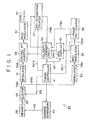
- Fig. 1 is a block diagram showing the modulating data generator 30 as well as the peripheral circuits.
- a timing controller 41 outputs a switching signal SEL to a selector 43 on the basis of a clock of the modulated data D6 processed in the modulating data generator 30, and outputs various timing signals necessary for operating an address generator 44. Further, the timing controller 41 outputs a sampling pulse SP to an NRZI sampler 45, and outputs reset pulses RST1 and RST2 that set one frame DSV counter 46 and DSV integrating counter 47, respectively, to the initial values.
- the address generator 44 is controlled by the timing controller 41 to output an address data AD to the memory 28. As shown in Fig. 3, the address generator 44 outputs in the time division an address data AD (A1) and an address data AD (A0, A1) precedent to the address data AD (A1) for one frame for the modulated data D6 to be recorded into the mmagneto-optic discoptical disc 21 (Fig. 3A). Thereby, the memory 28 is designed to output a modulated data DA1 to be recorded into the magneto-optic disc 21 precedently for one frame in each frame, and thereafter to output a modulated data DA0 to be recorded into the magneto-optic disc 21 (Fig. 3B).
- the selector 43 receives the modulated data D6 outputted from the memory 28, controlled by the timing controller 41, outputs a modulated data D6A precedent for one frame to a modulator 50 (Fig. 3C), and outputs a following modulated data D6B to a modulator 51 (Fig. 3D).
- the modulator 50 modulates the modulated data D6A (Fig. 4A) in accordance with the 1-7 modulation system, and outputs a modulating data D9A (Fig. 4C) formed of the NRZ (Non Return to Zero) code synchronized with a clock CK (Fig. 4B).
- An NRZI modulator 52 inverts the logical level at the timing that the logical level of the modulating data D9A falls down, and converts the modulating data D9A into a modulating data D10A formed of the NRZI (Non Return to Zero Inverted) code and outputs the data (Fig. 4D).
- the one frame DSV counter 46 increases or decreases the count value in correspondence with the logical level of the modulating data D10A, and thereby detects a DSV of the modulating data D10A (Fig. 4E). Further, when counting the DSV of the modulating data D10A corresponding to a control bit CT that is allocated to the synchronizing signal of the modulating data D9A, the one frame DSV counter 46 resets the count value by a reset pulse RST1 (Fig. 4F) outputted from the timing controller 41.
- the one frame DSV counter 46 detects the DSV of the modulating data D10A precedently for one frame, for the period from the control bit CT of the modulating data D9A through the following control bit CT. Further, the one frame DSV counter 46 generates a sign bit FBA (Fig. 4G) such that the logical level switches in accordance with the sign of the detected DSV, and outputs the sign bit FBA to a polarity judgment circuit 54.
- a sign bit FBA Fig. 4G
- the NRZI sampler 45 samples the modulating data D10A by the sampling pulse SP (Fig. 4H) outputted from the timing controller 41, and outputs a sampled result SPA (Fig. 4I) to the polarity judgment circuit 54.
- the control bit CT is held at a specific value
- the modulated data D6 read out precedently for one frame to the memory 28 is processed in the same manner as in recording, the DSV of the modulating data D10A thus obtained is detected in one frame, and on the basis of the sampling pulse SP, the sign of the modulating data D10A is detected.
- the modulator 51 in the same manner as the modulator 50, modulates the modulated data D6B and outputs the modulating data D9B (Fig. 4J).
- a control bit inverter 56 receives the modulating data D9B, and being controlled by the polarity judgment circuit 54, inverts the polarity of the control bit CT to output.
- the control bit inverter 56 sets the polarity of the control bit CT in compliance with the control signal outputted from the polarity judgment circuit 54.
- An NRZI modulator 57 receives the output data from the control bit inverter 56, and processes in the same manner as the NRZI modulator 52 to output the modulating data D7 (D10B) (Fig. 4K).
- the DSV integrating counter 47 after the count value is reset at the timing of start of modulation, sequentially integrates the DSV of the modulating data D7 (D10B) (Fig. 4L). Further, the DSV integrating circuit 47 generates the sign bit FBB (Fig. 4M) such that the logical level switches in accordance with the sign of the DSV, and outputs the sign bit FBB to the polarity judgment circuit 54. Thereby, in the modulating data generator 30, the DSV at the present moment is detected in addition to the detection of the DSV precedent for one frame and the sign detection of the modulating data D10A.
- the polarity judgment circuit 54 takes in and holds a detection result FBA (Fig. 5E) of the DSV detected from the modulating data D10A (Fig. 5C) and a sign detection result SPA (Fig. 5F). Thereby the polarity judgment circuit 54 detects and holds the dc level and polarity of the modulating data D10B (Fig. 5H) in advance from the modulated data D6A (Figs. 5A and 5B) precedent for one frame.
- FBA Fig. 5E
- a sign detection result SPA Fig. 5F
- the polarity judgment circuit 54 detects the polarity of the modulating data D10B (Fig. 5H) generated from the modulated data D6B (Fig. 5G) and a cumulatively added DSV at the present moment as a detection result FBB (Fig. 5J). Further, the polarity judgment circuit 54 judges to invert the polarity of the control bit CT or not according to the relation shown in Fig. 6, from the detection result FBA of the DSV detected in advance, the detection result FBB of the DSV at the present moment, and the sign detection results of the modulating data D10A and D10B.
- both the detection result FBA of the DSV precedent for one frame and the detection result FBB of the DSV at the present moment are held to the logical level "H", and the modulating data D10A and D10B both are held to the logical level "H"; and thereby, the polarity judgment circuit 54 sets the operation of the control bit inverter 56 so as to invert the control bit CT.
- the modulated data D6B (Fig. 5L) is modulated, while the polarity of the control bit CT is set so as to converge the DSV (Fig. 5K) at the present moment to the zero level, into the modulating data D10B by the NRZI code.
- the modulating data D10B (D7) generates the modulation magnetic field, and thereby the modulated data D6B is recorded into the magneto-optic disc 21.
- the user data D5 (Fig. 2) inputted from a computer or the like is inputted to the EDC encoder 25 in a specific block through the buffer memory 24, where the error detection code is added. Further, the user data D5 is scrambled in the scrambling circuit 26, and thereafter the ID encoder 27 adds a fixed data such as IDs to the user data D5, which is stored in the memory 28. To the data stored in the memory 28, the ECC 29 adds the error correction codes, thereby generating the modulated data D6.
- the preceding modulated data DA0 for one frame and the following modulated data DA1 for one frame are outputted from the memory 28 in the time division.
- the modulated data D6 is separated into the preceding modulated data D6A for one frame and the following modulated data D6B for one frame.
- the dc level of the modulating data is detected in advance by the modulated data D6A precedent for one frame, and the dc level of the modulating data is compensated.
- the preceding modulated data D6A is modulated in accordance with the 1-7 modulation system by the modulator 50, and thereafter is converted into the modulating data D10A by the following NRZI modulator 52.
- the one frame DSV counter 46 detects the DSV for one frame from a control bit (Fig. 4) to the next control bit and the sign (FBA) of the DSV to be outputted to the polarity judgment circuit 54.
- the NRZI sampler 45 detects the sign of the modulating data D10A by the sampling pulse SP that rises precedently for specific bits compared to the control bit CT.
- the detected result (SPA) is outputted to the polarity judgment circuit 54.
- the modulated data D6B is modulated in accordance with the 1-7 modulation system by the modulator 51, thereafter is inputted to the NRZI modulator 57 through the control bit inverter 56, and is converted therein into the modulating data D10B to be outputted to the driver 31.
- the accumulated DSV of the modulating data D10B is counted by the DSV integrating counter 47, and the DSV at the present moment is detected in correspondence with the DSV precedent for one frame detected by the one frame DSV counter 46.
- the polarity at the present moment is detected by the sampling pulse SP.
- control bit inverter 56 inverts the control bit CT so as to converge the DSV to zero, namely, to make the dc level into zero from the polarity and DSV detected at the present moment and the polarity and DSV detected precedently for one frame.
- the dc level of the modulating data D10B is compensated on the basis of the dc level detected in advance, which is outputted to the driver 31 (Fig. 2).
- the modulation coil 23 is driven by the modulating data D7 (D10B) and the quantity of the laser beams is raised intermittently; and thereby, the dc level is suppressed and the user data D5 is recorded into the magneto-optic disc 21 by the thermomagnetic recording system.
- the laser beams are irradiated from the optical pickup 22, and a change of the plane of polarization of the returned light is detected to generate the regenerative signal RF.
- the regenerative signal RF is converted into a binary signal in the demodulator circuit 33 and a regenerative clock is generated from the binary signal. Further, the binary signal is sequentially latched on the basis of the regenerative clock to generate a reproduced data.
- the regenerative signal RF is correctly converted into the binary signal, and the jitters, etc. of the regenerative clock are effectively suppressed, and further the bit errors are effectively reduced, thus correctly demodulating the reproduced data.
- the modulated data D6A precedent for one frame and the original modulated data D6B are outputted from the memory 28 in the time division, and thereafter separated and processed.
- the modulating data generator 30 can be used commonly to different systems.
- the foregoing embodiment deals with a case in which the DSV is detected precedently for one frame in advance.
- the invention is not limited to this and can widely be applied to a case in which the DSV is detected precedently for two frames or more, or further to a case in which the DSV is detected precedently for a period shorter than one frame.
- the foregoing embodiment deals with a case in which the dc level is compensated by inverting the control bit for one bit.
- the invention is not limited to this and can widely be applied to a case in which the operation of the NRZI modulator 57 may be switched at a timing corresponding to the control bit to compensate the dc level, or for example, to a case in which the polarity of the entire synchronizing signal is inverted to compensate the dc level.
- the foregoing embodiment discusses a case in which the modulated data is recorded in accordance with the 1-7 modulation system.
- the invention is not limited to this and can widely be applied to a case in which the modulated data is modulated in accordance with various PLL modulations.
- the foregoing embodiment deals with a case in which the user data is recorded into a magneto-optic disc.
- the invention is not limited to this and can widely be applied to a case in which a desired data is recorded into a phase change type optical disc, or further to a case in which various data are transmitted through transmission lines such as optical discs.
- the modulated data to be used for recording is supplied in the time division and the dc level is calculated in advance; and on the basis of the calculation result, the dc level is compensated to generate the modulating data.
- the dc level can be detected in advance with delay circuits omitted. Accordingly, the total construction of the system can be simplified to that extent, and the circuit blocks relating to the transmission system can be employed commonly to different systems.
Landscapes
- Engineering & Computer Science (AREA)
- Signal Processing (AREA)
- Computer Networks & Wireless Communication (AREA)
- Physics & Mathematics (AREA)
- Spectroscopy & Molecular Physics (AREA)
- Power Engineering (AREA)
- Signal Processing For Digital Recording And Reproducing (AREA)
Claims (3)
- Équipement de transmission de données, comprenant :un moyen de stockage (28) pour contenir des données modulées, et pour fournir dans une division temporelle des données modulées principales (D6B) utilisées pour la transmission et des données modulées subordonnées (D6A) précédant une période de référence spécifique aux données modulées principales ;un moyen de modulation principale (51, 56, 57) pour moduler les données modulées principales et générer des données de modulation principale (D10B),un moyen de détection de niveau de courant continu principal (47) pour détecter un niveau de courant continu des données de modulation principale et fournir un niveau de courant continu principal comme résultat de détection ;un moyen de modulation subordonnée (50, 52) pour moduler les données modulées subordonnées et générer des données de modulation subordonnée (D10A) par le même traitement que le moyen de modulation principale ;un moyen de détection de niveau de courant continu subordonné (46) pour détecter un niveau de courant continu des données de modulation subordonnée et fournir un niveau de courant continu subordonné comme un résultat de détection ; etun moyen de compensation de niveau de courant continu (54) pour commuter une opération du moyen de modulation principale et pour compenser le niveau de courant continu des données de modulation principale, sur la base des résultats de détection des niveaux de courant continu principal et subordonné.
- Équipement pour transmettre des données selon la revendication 1, dans lequel :le moyen de modulation principale (51, 56, 57) convertit les données modulées en données de modulation selon le code NRZ, et module ensuite lesdites données de démodulation en données de modulation principale du code NRZI ; etle moyen de compensation de niveau de courant continu (54) inverse un bit spécifique mis aux données de modulation du code NRZ et compense le niveau de courant continu des données de modulation principale.
- Procédé pour la transmission de données, le procédé comprenant les traitements de :maintien des données modulées, et fourniture dans une division temporelle des données modulées principales utilisées pour la transmission et des données modulées subordonnées précédentes pendant une période de référence spécifique pour les données modulées principales ;modulation des données modulées principales et génération des données de modulation principale par un moyen de modulation principale ;détection d'un niveau de courant continu des données de modulation principale et fourniture d'un niveau de courant continu principal comme résultat de détection ;modulation des données modulées subordonnées et génération des données de modulation subordonnée, par le même traitement que le moyen de modulation principale ;détection d'un niveau de courant continu des données de modulation subordonnée et fourniture d'un niveau de courant continu subordonné comme résultat de détection ; etcommutation d'une opération du moyen de modulation principale et compensation du niveau de courant continu des données de modulation principale, sur la base des résultats de détection des niveaux de courant continu principaux et subordonnés.
Applications Claiming Priority (3)
| Application Number | Priority Date | Filing Date | Title |
|---|---|---|---|
| JP26035096 | 1996-09-09 | ||
| JP260350/96 | 1996-09-09 | ||
| JP26035096A JP4032399B2 (ja) | 1996-09-09 | 1996-09-09 | 情報伝送装置、情報伝送方法及び光ディスク装置 |
Publications (3)
| Publication Number | Publication Date |
|---|---|
| EP0828247A2 EP0828247A2 (fr) | 1998-03-11 |
| EP0828247A3 EP0828247A3 (fr) | 1999-09-01 |
| EP0828247B1 true EP0828247B1 (fr) | 2004-08-04 |
Family
ID=17346749
Family Applications (1)
| Application Number | Title | Priority Date | Filing Date |
|---|---|---|---|
| EP97115346A Expired - Lifetime EP0828247B1 (fr) | 1996-09-09 | 1997-09-04 | Equipement de transmission de données et méthode associée |
Country Status (5)
| Country | Link |
|---|---|
| US (1) | US6049514A (fr) |
| EP (1) | EP0828247B1 (fr) |
| JP (1) | JP4032399B2 (fr) |
| KR (1) | KR100535292B1 (fr) |
| DE (1) | DE69730087T2 (fr) |
Families Citing this family (4)
| Publication number | Priority date | Publication date | Assignee | Title |
|---|---|---|---|---|
| CN1055143C (zh) * | 1998-07-24 | 2000-08-02 | 清华大学 | 氮化铝纤维的合成方法 |
| EP1280151A4 (fr) * | 2001-02-08 | 2007-08-08 | Sony Disc And Digital Solution | Generateur de signaux de modulation pour produire un disque original de disque optique |
| JP3714301B2 (ja) * | 2002-07-04 | 2005-11-09 | ソニー株式会社 | 記録装置、記録方法、再生装置、再生方法、及び記録媒体 |
| US7190653B2 (en) * | 2002-10-21 | 2007-03-13 | Ricoh Company, Ltd. | Data recording/reproducing device |
Family Cites Families (9)
| Publication number | Priority date | Publication date | Assignee | Title |
|---|---|---|---|---|
| JPS60669A (ja) * | 1983-06-17 | 1985-01-05 | Hitachi Ltd | デイジタル信号変調記録回路 |
| JPS60150735A (ja) * | 1984-01-18 | 1985-08-08 | 株式会社東芝 | 超音波診断装置 |
| US5333126A (en) * | 1990-01-03 | 1994-07-26 | Hitachi, Ltd. | Information recording method and optical disk apparatus using same |
| US5151699A (en) * | 1990-09-05 | 1992-09-29 | Pioneer Electronic Corporation | Data converting apparatus |
| JP2948016B2 (ja) * | 1992-03-19 | 1999-09-13 | 株式会社日立製作所 | 情報記録再生方法 |
| JPH06162668A (ja) * | 1992-11-24 | 1994-06-10 | Hitachi Ltd | 情報記録方式 |
| EP0660325B1 (fr) * | 1993-12-21 | 1999-11-10 | Sony Corporation | Méthode et appareil d'enregistrement de données sur un support d'enregistrement |
| JP3541439B2 (ja) * | 1994-07-08 | 2004-07-14 | ソニー株式会社 | 信号変調方法及び装置、並びに信号復調装置及び方法 |
| JP3794036B2 (ja) * | 1995-04-07 | 2006-07-05 | ソニー株式会社 | データの記録媒体及びデータ記録装置 |
-
1996
- 1996-09-09 JP JP26035096A patent/JP4032399B2/ja not_active Expired - Fee Related
-
1997
- 1997-09-04 US US08/923,342 patent/US6049514A/en not_active Expired - Fee Related
- 1997-09-04 DE DE69730087T patent/DE69730087T2/de not_active Expired - Lifetime
- 1997-09-04 EP EP97115346A patent/EP0828247B1/fr not_active Expired - Lifetime
- 1997-09-08 KR KR1019970046132A patent/KR100535292B1/ko not_active Expired - Fee Related
Also Published As
| Publication number | Publication date |
|---|---|
| US6049514A (en) | 2000-04-11 |
| EP0828247A2 (fr) | 1998-03-11 |
| DE69730087T2 (de) | 2005-08-11 |
| KR19980024420A (ko) | 1998-07-06 |
| JPH1083634A (ja) | 1998-03-31 |
| EP0828247A3 (fr) | 1999-09-01 |
| KR100535292B1 (ko) | 2006-03-16 |
| JP4032399B2 (ja) | 2008-01-16 |
| DE69730087D1 (de) | 2004-09-09 |
Similar Documents
| Publication | Publication Date | Title |
|---|---|---|
| US4716567A (en) | Method of transmitting digital data in which error detection codes are dispersed using alternate delay times | |
| EP0310330B1 (fr) | Dispositif d'enregistrement et de reproduction d'un signal numérique | |
| KR19990023617A (ko) | 기록 매체, 데이타 전송 장치, 데이타 수신 장치 및 광디스크 장치 | |
| US4456905A (en) | Method and apparatus for encoding binary data | |
| US4577180A (en) | Digital data converting method and apparatus thereof | |
| EP0828247B1 (fr) | Equipement de transmission de données et méthode associée | |
| US4680791A (en) | Digital video signal process apparatus for use in a video tape recorder | |
| JPH07326139A (ja) | 記録符号化ディジタル信号再生装置 | |
| US4516163A (en) | Digital information signal recording system | |
| US20020114460A1 (en) | Method of embedding a secondary signal in the bitstream of a primary signal | |
| EP0853805B1 (fr) | Transmission, enregistrement et reproduction d'un signal d'information numerique | |
| US5101394A (en) | Data reproducing apparatus | |
| US4868853A (en) | Demodulation circuit for digital modulated signal | |
| JP3239663B2 (ja) | 変調方法、変調装置及び復調装置 | |
| US4870647A (en) | Digital signal demodulator | |
| CN1042783C (zh) | 二进制信号判定电路 | |
| GB2243060A (en) | Disk drive controller. | |
| JP3144107B2 (ja) | 記録再生制御信号の伝送方法及び記録再生制御装置 | |
| KR0166753B1 (ko) | 드럼 가변회전수에 대응하는 디지탈 영상기록재생장치 및 그 방법 | |
| US6108149A (en) | Digital data transmitting apparatus for transmitting partial response signals | |
| KR100250577B1 (ko) | 비디오 씨디의 동기 검출장치 | |
| KR0152771B1 (ko) | 디지탈 자기기록/재생기의 에러검출장치 | |
| JP2870060B2 (ja) | 符号化方法 | |
| JP3276700B2 (ja) | ディスクのデータ記録方法およびディスクのデータ記録再生方法 | |
| JPH0758916B2 (ja) | デ−タ伝送装置 |
Legal Events
| Date | Code | Title | Description |
|---|---|---|---|
| PUAI | Public reference made under article 153(3) epc to a published international application that has entered the european phase |
Free format text: ORIGINAL CODE: 0009012 |
|
| AK | Designated contracting states |
Kind code of ref document: A2 Designated state(s): DE FR GB |
|
| PUAL | Search report despatched |
Free format text: ORIGINAL CODE: 0009013 |
|
| AK | Designated contracting states |
Kind code of ref document: A3 Designated state(s): AT BE CH DE DK ES FI FR GB GR IE IT LI LU MC NL PT SE |
|
| 17P | Request for examination filed |
Effective date: 20000105 |
|
| AKX | Designation fees paid |
Free format text: DE FR GB |
|
| 17Q | First examination report despatched |
Effective date: 20021230 |
|
| GRAP | Despatch of communication of intention to grant a patent |
Free format text: ORIGINAL CODE: EPIDOSNIGR1 |
|
| GRAS | Grant fee paid |
Free format text: ORIGINAL CODE: EPIDOSNIGR3 |
|
| GRAA | (expected) grant |
Free format text: ORIGINAL CODE: 0009210 |
|
| AK | Designated contracting states |
Kind code of ref document: B1 Designated state(s): DE FR GB |
|
| REG | Reference to a national code |
Ref country code: GB Ref legal event code: FG4D |
|
| REF | Corresponds to: |
Ref document number: 69730087 Country of ref document: DE Date of ref document: 20040909 Kind code of ref document: P |
|
| ET | Fr: translation filed | ||
| PLBE | No opposition filed within time limit |
Free format text: ORIGINAL CODE: 0009261 |
|
| STAA | Information on the status of an ep patent application or granted ep patent |
Free format text: STATUS: NO OPPOSITION FILED WITHIN TIME LIMIT |
|
| 26N | No opposition filed |
Effective date: 20050506 |
|
| PGFP | Annual fee paid to national office [announced via postgrant information from national office to epo] |
Ref country code: FR Payment date: 20080915 Year of fee payment: 12 |
|
| PGFP | Annual fee paid to national office [announced via postgrant information from national office to epo] |
Ref country code: GB Payment date: 20080910 Year of fee payment: 12 |
|
| PGFP | Annual fee paid to national office [announced via postgrant information from national office to epo] |
Ref country code: DE Payment date: 20090827 Year of fee payment: 13 |
|
| GBPC | Gb: european patent ceased through non-payment of renewal fee |
Effective date: 20090904 |
|
| REG | Reference to a national code |
Ref country code: FR Ref legal event code: ST Effective date: 20100531 |
|
| PG25 | Lapsed in a contracting state [announced via postgrant information from national office to epo] |
Ref country code: FR Free format text: LAPSE BECAUSE OF NON-PAYMENT OF DUE FEES Effective date: 20090930 |
|
| PG25 | Lapsed in a contracting state [announced via postgrant information from national office to epo] |
Ref country code: GB Free format text: LAPSE BECAUSE OF NON-PAYMENT OF DUE FEES Effective date: 20090904 |
|
| REG | Reference to a national code |
Ref country code: DE Ref legal event code: R119 Ref document number: 69730087 Country of ref document: DE Effective date: 20110401 |
|
| PG25 | Lapsed in a contracting state [announced via postgrant information from national office to epo] |
Ref country code: DE Free format text: LAPSE BECAUSE OF NON-PAYMENT OF DUE FEES Effective date: 20110401 |