EP0828359A2 - Empfänger für optische Burstsignale und Empfangsverfahren dazu - Google Patents
Empfänger für optische Burstsignale und Empfangsverfahren dazu Download PDFInfo
- Publication number
- EP0828359A2 EP0828359A2 EP97115625A EP97115625A EP0828359A2 EP 0828359 A2 EP0828359 A2 EP 0828359A2 EP 97115625 A EP97115625 A EP 97115625A EP 97115625 A EP97115625 A EP 97115625A EP 0828359 A2 EP0828359 A2 EP 0828359A2
- Authority
- EP
- European Patent Office
- Prior art keywords
- signal
- optical
- offset
- set forth
- receiving
- Prior art date
- Legal status (The legal status is an assumption and is not a legal conclusion. Google has not performed a legal analysis and makes no representation as to the accuracy of the status listed.)
- Withdrawn
Links
Images



Classifications
-
- H—ELECTRICITY
- H04—ELECTRIC COMMUNICATION TECHNIQUE
- H04B—TRANSMISSION
- H04B10/00—Transmission systems employing electromagnetic waves other than radio-waves, e.g. infrared, visible or ultraviolet light, or employing corpuscular radiation, e.g. quantum communication
- H04B10/60—Receivers
- H04B10/66—Non-coherent receivers, e.g. using direct detection
- H04B10/67—Optical arrangements in the receiver
-
- H—ELECTRICITY
- H04—ELECTRIC COMMUNICATION TECHNIQUE
- H04B—TRANSMISSION
- H04B10/00—Transmission systems employing electromagnetic waves other than radio-waves, e.g. infrared, visible or ultraviolet light, or employing corpuscular radiation, e.g. quantum communication
- H04B10/60—Receivers
- H04B10/66—Non-coherent receivers, e.g. using direct detection
- H04B10/69—Electrical arrangements in the receiver
- H04B10/695—Arrangements for optimizing the decision element in the receiver, e.g. by using automatic threshold control
Definitions
- the present invention relates to an optical receiver and an optical receiving method, and, more particularly, to an optical receiver for receiving optical burst signals and a receiving method for it.
- optical receivers for receiving optical burst signals include a device using an automatic threshold level control circuit ( hereinafter called the "ATC circuit").
- the optical receiver converts optical burst signals into electric current at its optical receiver element.
- the signal current is amplified, identified by the ATC circuit, and converted into digital signals by a limiter circuit (or, a limiter amplifier).
- An ATC circuit used for the above is disclosed, for example, in Japanese Patent Application Laid-Open No. 2-266630 (U.S. Patent No. 5,025,456).
- the ATC circuit sets a capacitor of a peak detector in it to an initial potential when an interval between optical burst signals is shorter than a leak time constant of the peak detector, so that subsequent optical burst signals can be surely received. For example, optical burst signal can be surely received by entering a reset signal to initialize the ATC circuit.
- the conventional optical receiver is known to be of a system not offsetting the threshold level of the ATC circuit (a circuit system setting the threshold value to zero) and a system offsetting the threshold level (a circuit system setting the threshold value to non-zero).
- both systems have the following problems.
- the system In the case of the system not offsetting threshold level of the ATC circuit, that is, setting the threshold level to zero in the reset operation, the system becomes a 1/0 uncertain state (a state where 1 or 0 is not determined) until the next optical burst signal. This state may erroneously establish synchronization.
- a limiter output outputs a noise signal even if there is no signal after a reset signal is input. This noise may cause erroneous operation of a circuit in the following stage.
- the present invention is intended to eliminate such problems, and to provide an optical receiver and an optical receiving method that do not offset the threshold level of the ATC circuit, thereby not deteriorating the minimum light receiving sensitivity and not outputting a noise signal when there is no signal.
- an optical receiver for receiving optical burst signals comprises an optical signal receiving section, an ATC circuit for identifying an electric signal output from the optical signal receiving section, a limiter circuit for outputting output of the ATC circuit as a digital signal, and offset optical signal generator means.
- the offset optical signal generator means comprises a control circuit for receiving a reset signal as input and outputting an offset signal, a circuit for driving a light emitting element with the offset signal, and the light emitting element for generating an offset optical signal.
- the automatic threshold level control circuit has an amplifier that does not offset the threshold level.
- the method for receiving optical burst signals first inputs a reset signal between optical burst signals, and inputs an offset signal immediately after the reset signal.
- the offset signal is entered as an optical signal into the optical signal receiving section of the optical receiver, and the reset signal is input as an electric signal to the ATC circuit that identifies an electric signal converted from an optical burst signal.
- An offset optical signal pulse is generated with the falling edge of the reset signal as a trigger. Its level is set lower than the minimum light receiving level of the incident optical signal.
- a conventional optical receiver is briefly described with reference to the drawing.
- a burst optical signal 5 is input into a light receiving element 1, and converted into electric current.
- the signal current is amplified by a preamplifier 2, identified by an ATC circuit 3, and converted into a digital signal by a limiter circuit 4.
- a reset signal 6 is input into the ATC circuit 3 to initialize it.
- the conventional optical receiver outputs a noise signal in no signal state when the threshold level of the ATC circuit is not offset, or deteriorates sensitivity when the threshold level of the ATC circuit is offset.
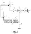
- FIG. 3 shows a configuration of an optical receiver according to the present invention.
- the optical receiver comprises a light receiving element 1 for being input with an optical burst signal 10 transmitted over fiber optics or the like, and a preamplifier 2 for amplifying an electric signal converted by the light receiving element 1, as well as comprises an ATC circuit 3 for identifying the amplified electric signal, and being input with a reset signal, and a limiter circuit 4 for receiving an output signal of the ATC circuit 3 and outputting a digital signal 12.
- the optical receiver further comprises offset optical signal generator means. In the example of FIG.
- the offset optical signal generator means comprises a control circuit 5 for being input with a reset signal 8, a light emitting element drive circuit 6 for connecting the control circuit 5 and driving a light emitting element 7, and the light emitting element 7 for inputting offset light into the light receiving element 1.
- FIG. 4 shows an embodiment of the ATC circuit 3.
- a peak detector (PEAKDET.) 26 connects an amplifier 21 to which a signal is input, and from which signals of forward and reverse phases are output.
- the peak detector 26 connects a capacitor 27 the other end of which is grounded, and a transistor 29 that connects a reference potential (V.RESET) 28, and to the base of which the reset signal 8 is input.
- the amplifier 21 used is a one without offset for the threshold level.
- the optical receiver of FIG. 3 and the ATC circuit 3 of FIG. 4 operate as follows.
- the optical burst signal 10 inputs in the light receiving element 1, the light receiving element 1 converts the optical burst signal into an electric signal.
- the electric signal is amplified by the preamplifier 2.
- the amplified electric signal is identified by the automatic threshold level control (ATC) circuit 3, and output as a digital signal 12 from the limiter circuit 4.
- ATC automatic threshold level control
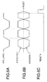
- the ATC circuit 3 when a signal as shown in FIG. 6A is input into an input terminal 33, an output waveform of the amplifier 21 becomes that as shown in FIG. 6B by the operation of the peak detector 26. Since the amplifier 21 used is a one without offset of the threshold level, there is no variation in the duty ratio regardless of the light receiving level.
- the reset signal 8 is also input into the control circuit 5 in addition to the ATC circuit 3.
- the control circuit 5 outputs the offset signal 9 with a predetermined width with the falling edge of the reset signal 8 as a trigger.
- the light emitting element drive circuit 6 drives the light emitting element 7 with the offset signal 9, and outputs an offset optical signal.
- the offset optical signal is input into the light receiving element 1 of the optical receiver.
- the light receiving level of the offset optical signal is desirably established to be lower than the minimum light receiving level of the optical input signal 10.
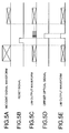
- FIGS. 5A to 5E the optical receiving method according to the present invention is described by referring to FIGS. 5A to 5E.
- a case is described where an optical burst signal with low light receiving level is entered following an optical burst signal with high light receiving level as shown in FIG. 3A.
- the reset signal 6 is generated between the burst optical signals to surely receive the optical burst signal with low light receiving level. Since the optical receiving method of the present invention is applied to the ATC circuit without offset, when the reset signal 6 is released, noise begins to be output on the output waveform of the limiter circuit (LIM.) 4, as shown in FIG. 5C.
- LIM. limiter circuit
- the control circuit 5 outputs the offset signal 9 with the falling edge of the reset signal 6 as a trigger.
- the offset optical signal 11 is entered into the light receiving element 1 for a specified period of time based on the offset signal 9.
- the optical burst signal is identified in a state where the offset signal is input between the optical burst signals.
- an output waveform 12 of the limiter circuit 4 becomes H-level under an operation similar to the input of the optical burst signal 10.
- the level of the offset optical signal 11 is set to be lower than the minimum light receiving level of the incident optical signal.
- the limiter circuit 4 When input of the offset optical signal 11 completes, the limiter circuit 4 continues to output L-level until the next optical burst signal 10 is entered. Since the level of the offset optical signal 11 is held by a capacitor 27 of the peak detector 26 in the ATC circuit 3, the limiter circuit 4 outputs zero (L-level). Generally, since a time constant of an offset cancel circuit (the time constant of the capacitor 27) is larger than the pulse width of the offset optical signal 11, the duration when L-level is output is longer than the pulse width. Consequently, a 1/0 uncertain state is avoided after completion of the reset signal 8, and there is no possibility that minute noise is output from the limiter circuit 4.
- timing when the reset signal is input into the ATC circuit after the first optical burst signal may be determined by taking into account time to the next optical burst signal, difference between light receiving levels, and the like.
- the offset optical signal 11 can be adjusted for its incident duration.
- the offset optical signal 11 can be masked by a circuit in the following stage.
- an interval between optical burst signals is, for example, about 8 to 16 bits, and width of reset and offset signals is adjusted to be about several bits.
- the present invention uses the ATC circuit not offsetting its threshold level, and inputs an offset optical signal at a level lower than the minimum light receiving level to the light receiving element with a reset signal as a trigger, so that the potential of the offset optical signal is held by the peak detector of the ATC circuit to vary the threshold level.
- the sensitivity is not deteriorated because a noise signal is not output in no signal state between the burst optical signals, and the duty ratio does not vary regardless of the light receiving level.
Landscapes
- Physics & Mathematics (AREA)
- Electromagnetism (AREA)
- Engineering & Computer Science (AREA)
- Computer Networks & Wireless Communication (AREA)
- Signal Processing (AREA)
- Optical Communication System (AREA)
Applications Claiming Priority (3)
| Application Number | Priority Date | Filing Date | Title |
|---|---|---|---|
| JP8239453A JP2891197B2 (ja) | 1996-09-10 | 1996-09-10 | 光受信方法および装置 |
| JP239453/96 | 1996-09-10 | ||
| JP23945396 | 1996-09-10 |
Publications (2)
| Publication Number | Publication Date |
|---|---|
| EP0828359A2 true EP0828359A2 (de) | 1998-03-11 |
| EP0828359A3 EP0828359A3 (de) | 2000-12-20 |
Family
ID=17044998
Family Applications (1)
| Application Number | Title | Priority Date | Filing Date |
|---|---|---|---|
| EP97115625A Withdrawn EP0828359A3 (de) | 1996-09-10 | 1997-09-09 | Empfänger für optische Burstsignale und Empfangsverfahren dazu |
Country Status (3)
| Country | Link |
|---|---|
| EP (1) | EP0828359A3 (de) |
| JP (1) | JP2891197B2 (de) |
| CA (1) | CA2214946A1 (de) |
Cited By (3)
| Publication number | Priority date | Publication date | Assignee | Title |
|---|---|---|---|---|
| EP1355436A1 (de) * | 2002-04-16 | 2003-10-22 | Samsung Electronics Co., Ltd. | Optischer Empfänger im Burstmodus zur Erzeugung eines Rücksetzsignals für eine automatische Schwellwertanpassungsschaltung zwischen aufeinanderfolgenden Bursts |
| EP1355437A1 (de) * | 2002-04-19 | 2003-10-22 | Samsung Electronics Co., Ltd. | Niedrigstwertdektor für einen optischen Empfänger im Burstbetrieb |
| US9191124B2 (en) | 2012-10-25 | 2015-11-17 | Avago Technologies General Ip (Singapore) Pte. Ltd. | Opto-isolator with correction circuit |
Families Citing this family (1)
| Publication number | Priority date | Publication date | Assignee | Title |
|---|---|---|---|---|
| JP4590708B2 (ja) * | 2000-09-26 | 2010-12-01 | 富士通株式会社 | 光受信回路 |
Family Cites Families (2)
| Publication number | Priority date | Publication date | Assignee | Title |
|---|---|---|---|---|
| US5025456A (en) * | 1989-02-02 | 1991-06-18 | At&T Bell Laboratories | Burst mode digital data receiver |
| US5371763A (en) * | 1992-11-13 | 1994-12-06 | At&T Corp. | Packet mode digital data receiver |
-
1996
- 1996-09-10 JP JP8239453A patent/JP2891197B2/ja not_active Expired - Lifetime
-
1997
- 1997-09-09 CA CA 2214946 patent/CA2214946A1/en not_active Abandoned
- 1997-09-09 EP EP97115625A patent/EP0828359A3/de not_active Withdrawn
Cited By (5)
| Publication number | Priority date | Publication date | Assignee | Title |
|---|---|---|---|---|
| EP1355436A1 (de) * | 2002-04-16 | 2003-10-22 | Samsung Electronics Co., Ltd. | Optischer Empfänger im Burstmodus zur Erzeugung eines Rücksetzsignals für eine automatische Schwellwertanpassungsschaltung zwischen aufeinanderfolgenden Bursts |
| US7266312B2 (en) | 2002-04-16 | 2007-09-04 | Samsung Electronics Co., Ltd. | Burst mode optical receiver |
| EP1355437A1 (de) * | 2002-04-19 | 2003-10-22 | Samsung Electronics Co., Ltd. | Niedrigstwertdektor für einen optischen Empfänger im Burstbetrieb |
| US7330670B2 (en) | 2002-04-19 | 2008-02-12 | Samsung Electronics Co., Ltd. | Bottom level detection device for burst mode optical receiver |
| US9191124B2 (en) | 2012-10-25 | 2015-11-17 | Avago Technologies General Ip (Singapore) Pte. Ltd. | Opto-isolator with correction circuit |
Also Published As
| Publication number | Publication date |
|---|---|
| EP0828359A3 (de) | 2000-12-20 |
| CA2214946A1 (en) | 1998-03-10 |
| JPH1084316A (ja) | 1998-03-31 |
| JP2891197B2 (ja) | 1999-05-17 |
Similar Documents
| Publication | Publication Date | Title |
|---|---|---|
| AU746734B2 (en) | Offset control for burst-mode optical receiver | |
| EP1615359B1 (de) | Infrarot-Kommunikationsanordnung | |
| EP0828359A2 (de) | Empfänger für optische Burstsignale und Empfangsverfahren dazu | |
| EP1315317A2 (de) | Vorrichtung zur Detektion von Unterbrechungen eines optischen Signals, optischen Empfängers, optischen Senders, und dazugehöriges Verfahren | |
| JP2003152649A (ja) | 光受信装置 | |
| US5712475A (en) | Light receiving circuit with variable threshold circuit | |
| US4692687A (en) | Optical pulse receiving device | |
| JP3031326B2 (ja) | バースト受信回路およびバースト受信回路の制御方法 | |
| US5302860A (en) | Circuit arrangement for automatic gain control | |
| JP2616480B2 (ja) | バースト光受信回路 | |
| JP2674494B2 (ja) | 光受信回路 | |
| JP3698988B2 (ja) | キャリア検出回路および赤外線リモコン受信機 | |
| JP2520455B2 (ja) | 相関ピ―ク検出回路 | |
| JP2536178B2 (ja) | 光送受信器 | |
| JP2917093B2 (ja) | 光モデム装置 | |
| EP0782264A2 (de) | Digitaler Empfänger mit adaptiven Schwellenwerten | |
| JPH0846568A (ja) | 光受信装置 | |
| JPH0340539A (ja) | 光信号入力断検出装置 | |
| JPH01149558A (ja) | 光伝送データ受信回路 | |
| JPH09260719A (ja) | 光受信回路 | |
| JP2545848B2 (ja) | 光受信回路 | |
| JPH08307358A (ja) | 光受信装置 | |
| JPH05252008A (ja) | 光受信回路 | |
| JPS595756A (ja) | 光入力断検知回路 | |
| JPH04350981A (ja) | レーザダイオード駆動電流設定装置 |
Legal Events
| Date | Code | Title | Description |
|---|---|---|---|
| PUAI | Public reference made under article 153(3) epc to a published international application that has entered the european phase |
Free format text: ORIGINAL CODE: 0009012 |
|
| AK | Designated contracting states |
Kind code of ref document: A2 Designated state(s): DE FR GB IT |
|
| PUAL | Search report despatched |
Free format text: ORIGINAL CODE: 0009013 |
|
| AK | Designated contracting states |
Kind code of ref document: A3 Designated state(s): AT BE CH DE DK ES FI FR GB GR IE IT LI LU MC NL PT SE |
|
| 17P | Request for examination filed |
Effective date: 20001108 |
|
| AKX | Designation fees paid |
Free format text: DE FR GB IT |
|
| STAA | Information on the status of an ep patent application or granted ep patent |
Free format text: STATUS: THE APPLICATION HAS BEEN WITHDRAWN |
|
| 18W | Application withdrawn |
Withdrawal date: 20020206 |