EP0830013A2 - Methode zur Kalibration eines Bildebenenarrays - Google Patents
Methode zur Kalibration eines Bildebenenarrays Download PDFInfo
- Publication number
- EP0830013A2 EP0830013A2 EP97114312A EP97114312A EP0830013A2 EP 0830013 A2 EP0830013 A2 EP 0830013A2 EP 97114312 A EP97114312 A EP 97114312A EP 97114312 A EP97114312 A EP 97114312A EP 0830013 A2 EP0830013 A2 EP 0830013A2
- Authority
- EP
- European Patent Office
- Prior art keywords
- detector element
- detector
- power level
- adjacent
- gain
- Prior art date
- Legal status (The legal status is an assumption and is not a legal conclusion. Google has not performed a legal analysis and makes no representation as to the accuracy of the status listed.)
- Withdrawn
Links
Images
Classifications
-
- H—ELECTRICITY
- H04—ELECTRIC COMMUNICATION TECHNIQUE
- H04N—PICTORIAL COMMUNICATION, e.g. TELEVISION
- H04N25/00—Circuitry of solid-state image sensors [SSIS]; Control thereof
- H04N25/60—Noise processing, e.g. detecting, correcting, reducing or removing noise
- H04N25/67—Noise processing, e.g. detecting, correcting, reducing or removing noise applied to fixed-pattern noise, e.g. non-uniformity of response
- H04N25/671—Noise processing, e.g. detecting, correcting, reducing or removing noise applied to fixed-pattern noise, e.g. non-uniformity of response for non-uniformity detection or correction
- H04N25/673—Noise processing, e.g. detecting, correcting, reducing or removing noise applied to fixed-pattern noise, e.g. non-uniformity of response for non-uniformity detection or correction by using reference sources
-
- H—ELECTRICITY
- H04—ELECTRIC COMMUNICATION TECHNIQUE
- H04N—PICTORIAL COMMUNICATION, e.g. TELEVISION
- H04N23/00—Cameras or camera modules comprising electronic image sensors; Control thereof
- H04N23/20—Cameras or camera modules comprising electronic image sensors; Control thereof for generating image signals from infrared radiation only
-
- H—ELECTRICITY
- H04—ELECTRIC COMMUNICATION TECHNIQUE
- H04N—PICTORIAL COMMUNICATION, e.g. TELEVISION
- H04N25/00—Circuitry of solid-state image sensors [SSIS]; Control thereof
- H04N25/48—Increasing resolution by shifting the sensor relative to the scene
Definitions
- the invention relates to the field of focal plane array sensors (FPA) and in particular to focal place array flat-field calibration by a cross-pixel step-stare reflector.
- FPA focal plane array sensors
- Focal plane arrays are optical sensing devices utilized in imaging and night vision devices such as the forward looking infrared (FLIR) systems, surveillance systems, and sensory/tracking systems for weapon control.
- FLIR forward looking infrared
- FPAs are particularly useful in detecting weak objects or objects whose emitted radiation has been strongly attenuated by atmospheric conditions.
- Stare FPA scanning devices i.e., devices having multiple detector elements assembled into an array, include a two-dimensional array of elements which simultaneously receive information from an area within the field of view of the FPA utilizing electronic scanning.
- An optical scanning assembly scans the field of view at a number of different viewing angles and reflects the signals received from a particular viewing angle to the scanning array.
- the optical scanning assembly can include oscillating mirrors or vertically and horizontally rotating prisms to hold or "stare” while scanning at a particular viewing angle and then move or "step” to a new viewing angle, scanning at this new viewing angle and so on.
- Flat-field calibration sources are usually difficult to include in the imaging optics system because limitations in space and cost. This is particularly the case for long wave applications.
- passive millimeter wave imaging technology providing visibility in obscured weather such as in fog, rain and snow, require substantially simplified and improved calibration, for both pixel gains and offsets.
- the present invention satisfies these needs.
- the present invention provides a method of calibrating gains and offsets for a two-dimensional detector array comprising individual detector elements.
- the method comprises the steps of: focusing a first incoming image signal at a first power level onto the detector array; reading the corresponding electrical signals from the detector elements as a first image frame at the first power level; for each detector element, translating the first incoming image signal by a detector element distance onto an adjacent detector element; reading the corresponding electrical signal from the detector elements as a second image frame at the first power level; focusing a second incoming image signal at a second power level onto the detector array; reading the corresponding electrical signals from the detector elements as a first image frame at the second power level; for each detector element, translating the second incoming image signal by a detector element distance onto an adjacent detector element; and reading the corresponding electrical signals from the detector elements as a second image frame at the second power level.
- the method further comprises the steps of: selecting a reference detector element; determining the gain of detector elements adjacent to the reference detector element from: (1) the corresponding electrical signals of the reference detector element and said adjacent detector elements from the first and the second images at the first and the second power levels, respectively, and (2) the gain of the reference detector element; and determining the offset of said adjacent detector elements from: (1) the corresponding electrical signals of the reference detector element and said adjacent detector elements from the first and second image frames at the first power level, (2) the gain of the reference detector element, (3) the offset of the reference detector element, and (4) the gain of said adjacent detector elements.
- the selection and determination steps can be repeated for all detector elements of the detector array.
- the present invention also provides a computer software system including program instructions implementing the method of the present invention.
- the present invention also provides a focal plane array calibration system for calibrating the gains and offsets for a two-dimensional detector array comprising individual detector elements.
- the system comprises: an optical assembly for focusing incoming image signals onto the detector array; an input system for reading the corresponding electrical signals from the detector elements; and a controller for controlling the optical assembly and the input system for: focusing a first incoming image signal at a first power level onto the detector array; reading the corresponding electrical signals from the detector elements as a first image frame at the first power level; translating the first incoming image signal by a detector element distance onto an adjacent detector element for each detector element; reading the corresponding electrical signals from the detector elements as a second image frame at the first power level; focusing a second incoming image signal at a second power level onto the detector array; reading the corresponding electrical signals from the detector elements as a first image frame at the second power level; translating the second incoming image signal by a detector element distance onto an adjacent detector element for each detector element; and reading the corresponding electrical signals from the detector elements as a second image frame
- the system further comprises a processor for: selecting a reference detector element; determining the gain of detector elements adjacent to the reference detector element from: (1) the corresponding electrical signals of the reference detector element and said adjacent detector elements from the first and the second images at the first and the second power levels, respectively, and (2) the gain of the reference detector element; and determining the offset of said adjacent detector elements from: (1) the corresponding electrical signals of the reference detector element and said adjacent detector elements from the first and second image frames at the second power level, (2) the gain of the reference detector element, (3) the offset of the reference detector element, and (4) the gain of said adjacent detector elements.
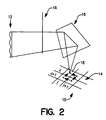
- a method of calibrating gains and offsets for a two-dimensional detector array 10 includes the high level steps of focusing the image of a calibration source 12 at a source power level onto the detector elements 14 of the two-dimensional detector array 10. Resulting electrical signals from the detector elements 14 are stored in a memory device. The image of calibration source 12 is then translated by one or more pixel distance, by a step-stare reflector assembly 16, so that the same illumination effect is produced on the adjacent detector of every detector element 14. The electrical signals from the detector elements 14 are compared with the stored values to obtain offset and gain calibration.
- the method of the present invention comprises the steps of: focusing a first incoming image signal at a first power level onto the detector array 10; reading the corresponding electrical signals from the detector elements 14 as a first image frame at the first power level; for each detector element 14, translating the first incoming image signal by a detector element distance onto an adjacent detector element 14; reading the corresponding electrical signal from the detector elements 14 as a second image frame at the first power level; focusing a second incoming image signal at a second power level onto the detector array 10; reading the corresponding electrical signals from the detector elements 14 as a first image frame at the second power level; for each detector element 14, translating the second incoming image signal by a detector element distance onto an adjacent detector element 14; and reading the corresponding electrical signals from the detector elements 14 as a second image frame at the second power level.
- the method further comprises the steps of: selecting a reference detector element 14; determining the gain of detector elements adjacent to the reference detector element 14 from: (1) the corresponding electrical signals of the reference detector element 14 and said adjacent detector elements from the first and the second image frames at the first and the second power levels, respectively, and (2) the gain of the reference detector element 14; and determining the offset of said adjacent detector elements from: (1) the corresponding electrical signals of the reference detector element 14 and said adjacent detector elements from the first and second image frames at the first power level, (2) the gain of the reference detector element 14, (3) the offset of the reference detector element 14, and (4) the gain of said adjacent detector elements.
- the selection and determination steps can be repeated for all detector elements of the detector array.
- an FPA calibration method utilizes a step-stare reflector 16 with an unspecified noise source 12.
- An FPA 10 is an orthogonal, two-dimensional detector array with NXM detectors 14.
- the detectors 14 can be visible light, infrared, millimeter wave or microwave sensors.
- the natural background source is sufficient.
- a switch noise source with illumination power slightly higher than the background radiation is used for pixel gain calibration. In both cases, advantageously, source uniformity and knowledge of the source function amplitude are not required.
- the first step includes focusing the image signal of the switching calibration source 12 at the first power level onto the FPA 10, then digitizing and recording the corresponding electrical signal levels for the entire FPA 10 as a first image frame at the first source power level.
- the second step includes translating horizontally (vertically) the image signal of the switching calibration source 12 at the first power level by one pixel distance to the left (top), so the adjacent detector element to the left (top) of every element 14 on the FPA 10, except the one on the left (top) edge of the FPA 10, observes the same image as that observed by a reference element 18 in the first step, then digitizing and recording the corresponding electrical signals for the entire FPA as a second image frame at the first source power level.
- the third step includes focusing the image signal of the switching calibration source 12 at the second power level on to the FPA 10, then digitizing and recording the corresponding electrical signal levels for the entire FPA 10 as a first image frame at the second source power level.
- the fourth step includes translating horizontally (vertically) the image signal of the switching calibration source 12 at the second power level one pixel distance to the right (down), so the adjacent detector element to the top (bottom) of every element on the FPA 10, except the one on the right (bottom) edge of the FPA, observes the same image as that observed by the reference element 18 in the third step, then digitizing and recording the corresponding electrical signal levels as the second image frame at the second source power level.
- the fifth step includes determining the gain of every adjacent detector element 14 from: (1) the ratio of the difference of the electrical signals observed by the reference detector element 18 under the two source power levels used to the difference of that observed by the adjacent detectors 14 under the same source power levels, and (2) the gain of the reference detector 18.
- the sixth step includes determining the offset of every adjacent detector element 14 from; (1) the corresponding electrical signals observed by the adjacent detector element 14 and the reference detector 18 under the same source power level, (2) the gain of the reference detector 18, (3) the offset of the reference detector 18, and (4)the gain of the adjacent detector element 14.
- the above steps are repeated for all detector elements 14 of the FPA 10 except one.
- the one detector which has no other detector to refer to will be calibrated in a separated procedure.
- the detectors 14 are arranged in the form of a two-dimensional array with NxM pixel elements, or a NxM FPA.
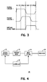
- the image observed by a reference pixel (i,j) is moved to walk through the neighboring three pixels, (i+1,j), (i+1,j+1) and (i,j+1), in a 4-step cycle and the switching source 12 is synchronized with the step-stare motion, as shown in Fig. 3.
- relation (5) expresses all pixel gains in terms of the gain of the first pixel.
- the step-stare reflector 16 is utilized to achieve offset and gain calibration of the FPA 10.
- the step-stare reflector 16 is used to move the image over the FPA 10 by exactly one pixel (per step) in each field of view (FOV) dimensions to an accuracy specified by the calibration requirement.
- FOV field of view
- the reflector 16 provides a physically identical illumination for every adjacent pixel pair, thereby allowing a quantitative comparison for the offset and gain of these two pixels.
- the offset and gain comparison between the adjacent pixel pair can be cascaded from one end to the other in the direction of the step-stare motion.
- the gain and offset calibration for the entire FPA 10 can be obtained without using a flat (uniform) calibration source.
- a two-dimensional step-stare reflector is used to obtain two-dimensional FPA 10 calibration.
- the presence of a few isolated bad pixels does not impair the cascaded calibration method because calibration beyond those bad pixels in one dimension (i.e. the x dimension) can be cascaded from the other dimension (i.e. the y dimension).
- cascaded calibration includes utilizing the step-stare reflector 16 to move an incoming image signal in a four-step cyclic motion in the following manner:
- the method of the present invention can be implemented as a computer software system for a dedicated processor, such as an TMS 320C50, or a general purpose computer such as a personal computer.
- the steps of the method of the present invention can be programmed as program instructions utilizing a program language such as C as is well known to the practitioners in the art.
- the mathematical relations can be implemented utilizing a simulation package of a math library readily available.
- the present invention provides a focal plane array calibration system 20 for calibrating the gains and offsets for a two-dimensional detector array 10 comprising individual detector elements shown in Fig. 4.
- the system 20 comprises: an optical assembly 22 for focusing incoming image signals onto the detector array 10; an input system 24 for reading the corresponding electrical signals from the detector elements 14; and a controller 26 for controlling the optical assembly 22 and the input system 24 for: focusing a first incoming image signal at a first power level onto the detector array 10; reading the corresponding electrical signals from the detector elements 14 as a first image frame at the first power level; translating the first incoming image signal by a detector element distance onto an adjacent detector element 14 for each detector element; reading the corresponding electrical signals from the detector elements 14 as a second image frame at the first power level; focusing a second incoming image signal at a second power level onto the detector array 10; reading the corresponding electrical signals from the detector elements 14 as a first image frame at the second power level; translating the second incoming image signal by a detector element distance onto an adjacent detector element for
- the system 20 further comprises a processor 28 for: selecting a reference detector element 18; determining the gain of detector elements 14 adjacent to the reference detector element 18 from: (1) the corresponding electrical signals of the reference detector element 18 and said adjacent detector elements 14 from the first and the second images at the first and the second power levels, respectively, and (2) the gain of the reference detector element 18; and determining the offset of said adjacent detector elements 14 from: (1) the corresponding electrical signals of the reference detector element 18 and said adjacent detector elements 14 from the first and second image frames at the second power level, (2) the gain of the reference detector element 18, (3) the offset of the reference detector element 18, and (4) the gain of said adjacent detector elements 14.
- the optical assembly 22, the detector array 10, the input system 24 and the controller 26 are well-known to the art and, therefore, described as an example below.
- the method of the present invention described herein and shown in the drawings can be used as a pseudo code for programming a general purpose or dedicated computer system.
- Example computer systems suitable for use with the present invention are described in the example below.
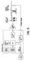
- step-stare reflector An example step-stare reflector is described here. Although the present invention does not depend on a particular mechanism of the step-stare reflector used, the calibration accuracy indeed depends strongly on the image position and alignment accuracy of the reflector.
- a block diagram for the step-stare reflector mechanism is shown in Fig. 5.
- the reflector is made of a light weight (0.75 lbs.), 10"x11.5"x0.5" honeycomb aluminum plate for millimeter wave application (at 90 Ghz). The surface flatness is maintained to within 1/10 of the wavelength which is 0.133.”
- the plate is supported at the center using two double-end flexure pivots, Model Lucas 6008-400, with high radial stiffness (22,000 lbs./in) and small spring rate (0.114 lb./in/degree).
- the motion of the reflector is actuated using four high quality voice-coil actuators, Model EBI LA15-15-000, with a force constant 1.35 lb./Amp.
- the actuator coils have time response faster than 100 micro-seconds, allowing close simulation of the actuator waveform in the frequency range from DC to above 20 kHz.
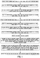
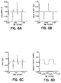
- a current waveform model can be used to produce the required step-stare motion: (1) moving the image from position P ij , P i+1j , P ji+1j+1 , and positioning P ij+1 in a four-step cyclic motion; (2) timing all motions to take place in less than 5 milliseconds, following a 10 millisecond motionless dwell time; (3) achieving position accuracy of less than 0.1 pixel distance; and (4) achieving timing accuracy of better than 0.1 milliseconds.
- a summary of current waveform is given in Fig. 6.
- B relates to the back electromotive force (EMF) by the actuator coils,
- K is the characteristic spring rate and
- N(t) is the required current waveform for the actuator torque.
- This waveform can be obtained by differentiating the desired position profile ⁇ (t), as shown in relation 6.
- N(t) can be modeled using a few scaling parameters and numerically integrated relation 6 to obtain ⁇ (t).
- the latter approach defines the relationship between the damping coefficient B and the back EMF.
- B K F 2 L
- K F is the same force constant of the actuator voice-coil
- L is the effective arm-length.
- Solution N(t) can be optimized by a number of trade-offs, including the peak force magnitude, the rise time requirement, the accuracy requirement, the power consumption requirement, etc.
- a Texas Instruments model TMS320C5X digital signal processing (DSP) Kit can be used for the control of the actuators and the data acquisition from the position sensors.
- the actuator current waveform is pre-loaded into the circular buffer of the TMS320C5CX PROM.
- This waveform is sequentially read into the driver program to generate a voltage drive signal through the on-board analog interface circuit model TLC32040C, which includes a 14-bit bipolar DAC and a dual channel 14 bit ADC.
- the output of the DAC is buffered and applied through two Model APEX 12PA power amplifiers to the actuators.
- the current phases of the four actuators were arranged to generate the four-step step-stare motion as follows: Referring to actuator 1 (zero phase), actuator 2 lags 90°, actuator 3 lags 180° and actuator 4 lags 270°.
- the on-board ADC are used to monitor the position sensor signals to provide precision control for the actuator balance positions.
- the mechanism of the millimeter-wave step-stare reflector described herein can be applied to other optics bands with shorter or longer wavelengths.
Landscapes
- Engineering & Computer Science (AREA)
- Multimedia (AREA)
- Signal Processing (AREA)
- Transforming Light Signals Into Electric Signals (AREA)
- Photometry And Measurement Of Optical Pulse Characteristics (AREA)
Applications Claiming Priority (2)
| Application Number | Priority Date | Filing Date | Title |
|---|---|---|---|
| US712757 | 1991-06-10 | ||
| US08/712,757 US5789622A (en) | 1996-09-12 | 1996-09-12 | Focal plane array calibration method |
Publications (2)
| Publication Number | Publication Date |
|---|---|
| EP0830013A2 true EP0830013A2 (de) | 1998-03-18 |
| EP0830013A3 EP0830013A3 (de) | 1999-10-13 |
Family
ID=24863437
Family Applications (1)
| Application Number | Title | Priority Date | Filing Date |
|---|---|---|---|
| EP97114312A Withdrawn EP0830013A3 (de) | 1996-09-12 | 1997-08-19 | Methode zur Kalibration eines Bildebenenarrays |
Country Status (4)
| Country | Link |
|---|---|
| US (1) | US5789622A (de) |
| EP (1) | EP0830013A3 (de) |
| JP (1) | JP3017140B2 (de) |
| CN (1) | CN1176380A (de) |
Cited By (4)
| Publication number | Priority date | Publication date | Assignee | Title |
|---|---|---|---|---|
| EP1253779A1 (de) * | 2001-04-25 | 2002-10-30 | Lockheed Martin Corporation | Szenenabhängige Korrektur der Ungleichmässigkeit von Detektoranordnungen |
| US6973218B2 (en) | 2001-04-25 | 2005-12-06 | Lockheed Martin Corporation | Dynamic range compression |
| US7103235B2 (en) | 2001-04-25 | 2006-09-05 | Lockheed Martin Corporation | Extended range image processing for electro-optical systems |
| EP2257047A4 (de) * | 2008-02-29 | 2015-12-30 | Nec Corp | Infrarot-bildgebungsvorrichtung und eigenrauschkorrekturverfahren |
Families Citing this family (15)
| Publication number | Priority date | Publication date | Assignee | Title |
|---|---|---|---|---|
| US5925875A (en) * | 1996-04-26 | 1999-07-20 | Lockheed Martin Ir Imaging Systems | Apparatus and method for compensating for fixed pattern noise in planar arrays |
| US6125335A (en) * | 1998-04-10 | 2000-09-26 | Sun Nuclear Corporation | Wide field calibration of a multi-sensor array |
| US6670596B2 (en) * | 2001-08-06 | 2003-12-30 | Raytheon Company | Radiometry calibration system and method for electro-optical sensors |
| US6900438B2 (en) * | 2003-01-31 | 2005-05-31 | Millivision Technologies | Baseline compensating method and camera used in millimeter wave imaging |
| US6870162B1 (en) * | 2003-01-31 | 2005-03-22 | Millivision, Inc. | Weighted noise compensating method and camera used in millimeter wave imaging |
| US6878939B2 (en) * | 2003-01-31 | 2005-04-12 | Millivision Technologies | Offset drift compensating flat fielding method and camera used in millimeter wave imaging |
| DE102006000976A1 (de) * | 2006-01-07 | 2007-07-12 | Leica Microsystems Cms Gmbh | Vorrichtung, Mikroskop mit Vorrichtung und Verfahren zum Kalibrieren eines Photosensor-Chips |
| EP2608713A4 (de) | 2010-08-27 | 2014-01-08 | Milwaukee Electric Tool Corp | Wärmeerkennungssysteme, -verfahren und -vorrichtungen |
| WO2012125819A2 (en) | 2011-03-15 | 2012-09-20 | Milwaukee Electric Tool Corporation | Thermal imager |
| US10794769B2 (en) * | 2012-08-02 | 2020-10-06 | Milwaukee Electric Tool Corporation | Thermal detection systems, methods, and devices |
| EP3183872B1 (de) * | 2014-08-20 | 2018-12-19 | Seek Thermal, Inc. | Adaptive regelung der betriebsspannung eines bildgebungssystems |
| US9641772B2 (en) | 2014-11-19 | 2017-05-02 | Northrop Grumman Systems Corporation | Compact PMMW camera calibration target |
| CN108088570B (zh) * | 2016-11-23 | 2020-02-21 | 北京遥感设备研究所 | 一种基于相控阵扫描体制的辐射计成像方法 |
| US10264191B2 (en) * | 2017-08-03 | 2019-04-16 | The Boeing Company | Calibration of pixels for producing super resolution images |
| CN113848592A (zh) * | 2020-06-28 | 2021-12-28 | 同方威视技术股份有限公司 | 安检系统、太赫兹波成像设备及其校准方法 |
Family Cites Families (17)
| Publication number | Priority date | Publication date | Assignee | Title |
|---|---|---|---|---|
| US4323987A (en) * | 1980-03-28 | 1982-04-06 | Pitney Bowes Inc. | Power failure memory support system |
| GB2149605B (en) * | 1983-11-04 | 1987-06-10 | Marconi Avionics | Image processing |
| GB2149260B (en) * | 1983-11-04 | 1987-05-13 | Marconi Avionics | Image processing |
| US4767937A (en) * | 1986-12-30 | 1988-08-30 | The Boeing Company | Scanning system with low scan rate and high effective frame rate |
| US4893925A (en) * | 1988-05-26 | 1990-01-16 | Grumman Aerospace Corporation | Optical measurement system for a display interface unit |
| US5001650A (en) * | 1989-04-10 | 1991-03-19 | Hughes Aircraft Company | Method and apparatus for search and tracking |
| US5140147A (en) * | 1990-08-14 | 1992-08-18 | Texas Instruments Incorporated | Intrafield interleaved sampled video processor/reformatter |
| US5129595A (en) * | 1991-07-03 | 1992-07-14 | Alliant Techsystems Inc. | Focal plane array seeker for projectiles |
| US5245425A (en) * | 1992-03-24 | 1993-09-14 | Hughes Aircraft Company | Method and apparatus for equalizing the gain of multi-channel systems in the presence of noise |
| EP0569063B1 (de) * | 1992-05-04 | 1998-06-03 | Agfa-Gevaert N.V. | Automatische Verschiebung und Verstärkungssteuerung für einen Dokumentenabtaster |
| WO1994000950A1 (en) * | 1992-06-19 | 1994-01-06 | Honeywell Inc. | Infrared camera with thermoelectric temperature stabilization |
| US5300780A (en) * | 1992-12-17 | 1994-04-05 | Trw Inc. | Missile surveillance method and apparatus |
| US5345304A (en) * | 1992-12-17 | 1994-09-06 | Texas Instruments Incorporated | Integrated LADAR/FLIR sensor |
| US5424543A (en) * | 1993-04-19 | 1995-06-13 | Surface Optics Corporation | Imaging spectroradiometer |
| US5390040A (en) * | 1994-02-04 | 1995-02-14 | Martin Marietta Corporation | Optical transceiver for free-space communication links |
| US5514865A (en) * | 1994-06-10 | 1996-05-07 | Westinghouse Electric Corp. | Dither image scanner with compensation for individual detector response and gain correction |
| JP3344163B2 (ja) * | 1995-06-06 | 2002-11-11 | 三菱電機株式会社 | 赤外線撮像素子 |
-
1996
- 1996-09-12 US US08/712,757 patent/US5789622A/en not_active Expired - Fee Related
-
1997
- 1997-08-19 EP EP97114312A patent/EP0830013A3/de not_active Withdrawn
- 1997-09-10 JP JP9244948A patent/JP3017140B2/ja not_active Expired - Lifetime
- 1997-09-11 CN CN97118435.6A patent/CN1176380A/zh active Pending
Cited By (6)
| Publication number | Priority date | Publication date | Assignee | Title |
|---|---|---|---|---|
| EP1253779A1 (de) * | 2001-04-25 | 2002-10-30 | Lockheed Martin Corporation | Szenenabhängige Korrektur der Ungleichmässigkeit von Detektoranordnungen |
| US6901173B2 (en) | 2001-04-25 | 2005-05-31 | Lockheed Martin Corporation | Scene-based non-uniformity correction for detector arrays |
| US6973218B2 (en) | 2001-04-25 | 2005-12-06 | Lockheed Martin Corporation | Dynamic range compression |
| US7103235B2 (en) | 2001-04-25 | 2006-09-05 | Lockheed Martin Corporation | Extended range image processing for electro-optical systems |
| US7760965B2 (en) | 2001-04-25 | 2010-07-20 | Lockheed Martin Corporation | Extended range image processing for electro-optical systems |
| EP2257047A4 (de) * | 2008-02-29 | 2015-12-30 | Nec Corp | Infrarot-bildgebungsvorrichtung und eigenrauschkorrekturverfahren |
Also Published As
| Publication number | Publication date |
|---|---|
| US5789622A (en) | 1998-08-04 |
| EP0830013A3 (de) | 1999-10-13 |
| JPH1090059A (ja) | 1998-04-10 |
| JP3017140B2 (ja) | 2000-03-06 |
| CN1176380A (zh) | 1998-03-18 |
Similar Documents
| Publication | Publication Date | Title |
|---|---|---|
| US5789622A (en) | Focal plane array calibration method | |
| US10267915B2 (en) | Optical system for object detection and location | |
| CA3017811C (en) | Lidar based 3-d imaging with varying pulse repetition | |
| US10908266B2 (en) | Time of flight distance sensor | |
| US4419692A (en) | High speed infrared imaging system | |
| EP3433578A1 (de) | Auf lidar basierende 3d-bildgebung mit variierender beleuchtungsintensität | |
| EP3433634A1 (de) | Auf lidar basierende 3d-bildgebung mit variierender beleuchtungsfelddichte | |
| JP2002525685A (ja) | プログラム可能レンズアッセンブリ及びこれを組み込んだ光学システム | |
| EP3602110B1 (de) | System und verfahren zur entfernungsmessung nach flugzeit | |
| US20210208283A1 (en) | Efficient algorithm for projecting world points to a rolling shutter image | |
| JP2578604B2 (ja) | ハンターとターゲットとの間の距離を測定するための光学的装置 | |
| US12163841B1 (en) | Systems and methods of acquiring polarization information | |
| US5086411A (en) | Optical location systems | |
| US11815676B2 (en) | Active pushbroom imaging system using a micro-electro-mechanical system (MEMS) micro-mirror array (MMA) | |
| US5600123A (en) | High-resolution extended field-of-view tracking apparatus and method | |
| Stanton et al. | CCD star sensor for fine pointing control of spaceborne telescopes | |
| JPH02500299A (ja) | 可変位相時間遅延及び信号集積システム及び走査検出装置の一定の空間分解能を得るための方法 | |
| JPH0949728A (ja) | 距離測定装置 | |
| JPH0798429A (ja) | 距離計測装置 | |
| CA2250451A1 (en) | Earth sensor | |
| Andresen et al. | Surface-based IRST: a selection process for sensor parameter values | |
| JP2680331B2 (ja) | 宇宙航行体の補捉追尾装置 | |
| JPH0624030B2 (ja) | 画像解析装置 | |
| Borghi et al. | Star detection and tracking using CCDs | |
| JPH10221110A (ja) | 太陽角度検出機能付き突き抜け走査型地球センサ |
Legal Events
| Date | Code | Title | Description |
|---|---|---|---|
| PUAI | Public reference made under article 153(3) epc to a published international application that has entered the european phase |
Free format text: ORIGINAL CODE: 0009012 |
|
| AK | Designated contracting states |
Kind code of ref document: A2 Designated state(s): AT BE CH DE DK ES FI FR GB GR IE IT LI LU MC NL PT SE |
|
| PUAL | Search report despatched |
Free format text: ORIGINAL CODE: 0009013 |
|
| AK | Designated contracting states |
Kind code of ref document: A3 Designated state(s): AT BE CH DE DK ES FI FR GB GR IE IT LI LU MC NL PT SE |
|
| STAA | Information on the status of an ep patent application or granted ep patent |
Free format text: STATUS: THE APPLICATION HAS BEEN WITHDRAWN |
|
| 18W | Application withdrawn |
Withdrawal date: 19991008 |