EP0831449A2 - Appareil de commande pour un dispositif d'affichage luminescent - Google Patents
Appareil de commande pour un dispositif d'affichage luminescent Download PDFInfo
- Publication number
- EP0831449A2 EP0831449A2 EP97305309A EP97305309A EP0831449A2 EP 0831449 A2 EP0831449 A2 EP 0831449A2 EP 97305309 A EP97305309 A EP 97305309A EP 97305309 A EP97305309 A EP 97305309A EP 0831449 A2 EP0831449 A2 EP 0831449A2
- Authority
- EP
- European Patent Office
- Prior art keywords
- pixel data
- data
- pixel
- drive
- image
- Prior art date
- Legal status (The legal status is an assumption and is not a legal conclusion. Google has not performed a legal analysis and makes no representation as to the accuracy of the status listed.)
- Withdrawn
Links
Images



Classifications
-
- G—PHYSICS
- G09—EDUCATION; CRYPTOGRAPHY; DISPLAY; ADVERTISING; SEALS
- G09G—ARRANGEMENTS OR CIRCUITS FOR CONTROL OF INDICATING DEVICES USING STATIC MEANS TO PRESENT VARIABLE INFORMATION
- G09G3/00—Control arrangements or circuits, of interest only in connection with visual indicators other than cathode-ray tubes
- G09G3/20—Control arrangements or circuits, of interest only in connection with visual indicators other than cathode-ray tubes for presentation of an assembly of a number of characters, e.g. a page, by composing the assembly by combination of individual elements arranged in a matrix no fixed position being assigned to or needed to be assigned to the individual characters or partial characters
- G09G3/2007—Display of intermediate tones
- G09G3/2044—Display of intermediate tones using dithering
- G09G3/2051—Display of intermediate tones using dithering with use of a spatial dither pattern
-
- G—PHYSICS
- G09—EDUCATION; CRYPTOGRAPHY; DISPLAY; ADVERTISING; SEALS
- G09G—ARRANGEMENTS OR CIRCUITS FOR CONTROL OF INDICATING DEVICES USING STATIC MEANS TO PRESENT VARIABLE INFORMATION
- G09G3/00—Control arrangements or circuits, of interest only in connection with visual indicators other than cathode-ray tubes
- G09G3/20—Control arrangements or circuits, of interest only in connection with visual indicators other than cathode-ray tubes for presentation of an assembly of a number of characters, e.g. a page, by composing the assembly by combination of individual elements arranged in a matrix no fixed position being assigned to or needed to be assigned to the individual characters or partial characters
- G09G3/22—Control arrangements or circuits, of interest only in connection with visual indicators other than cathode-ray tubes for presentation of an assembly of a number of characters, e.g. a page, by composing the assembly by combination of individual elements arranged in a matrix no fixed position being assigned to or needed to be assigned to the individual characters or partial characters using controlled light sources
- G09G3/28—Control arrangements or circuits, of interest only in connection with visual indicators other than cathode-ray tubes for presentation of an assembly of a number of characters, e.g. a page, by composing the assembly by combination of individual elements arranged in a matrix no fixed position being assigned to or needed to be assigned to the individual characters or partial characters using controlled light sources using luminous gas-discharge panels, e.g. plasma panels
- G09G3/2803—Display of gradations
-
- G—PHYSICS
- G09—EDUCATION; CRYPTOGRAPHY; DISPLAY; ADVERTISING; SEALS
- G09G—ARRANGEMENTS OR CIRCUITS FOR CONTROL OF INDICATING DEVICES USING STATIC MEANS TO PRESENT VARIABLE INFORMATION
- G09G2310/00—Command of the display device
- G09G2310/02—Addressing, scanning or driving the display screen or processing steps related thereto
- G09G2310/0229—De-interlacing
-
- G—PHYSICS
- G09—EDUCATION; CRYPTOGRAPHY; DISPLAY; ADVERTISING; SEALS
- G09G—ARRANGEMENTS OR CIRCUITS FOR CONTROL OF INDICATING DEVICES USING STATIC MEANS TO PRESENT VARIABLE INFORMATION
- G09G3/00—Control arrangements or circuits, of interest only in connection with visual indicators other than cathode-ray tubes
- G09G3/20—Control arrangements or circuits, of interest only in connection with visual indicators other than cathode-ray tubes for presentation of an assembly of a number of characters, e.g. a page, by composing the assembly by combination of individual elements arranged in a matrix no fixed position being assigned to or needed to be assigned to the individual characters or partial characters
- G09G3/22—Control arrangements or circuits, of interest only in connection with visual indicators other than cathode-ray tubes for presentation of an assembly of a number of characters, e.g. a page, by composing the assembly by combination of individual elements arranged in a matrix no fixed position being assigned to or needed to be assigned to the individual characters or partial characters using controlled light sources
- G09G3/28—Control arrangements or circuits, of interest only in connection with visual indicators other than cathode-ray tubes for presentation of an assembly of a number of characters, e.g. a page, by composing the assembly by combination of individual elements arranged in a matrix no fixed position being assigned to or needed to be assigned to the individual characters or partial characters using controlled light sources using luminous gas-discharge panels, e.g. plasma panels
- G09G3/288—Control arrangements or circuits, of interest only in connection with visual indicators other than cathode-ray tubes for presentation of an assembly of a number of characters, e.g. a page, by composing the assembly by combination of individual elements arranged in a matrix no fixed position being assigned to or needed to be assigned to the individual characters or partial characters using controlled light sources using luminous gas-discharge panels, e.g. plasma panels using AC panels
Definitions
- the present invention relates to a drive apparatus for a self light-emitting display unit
- sub-field method As a method of allowing a plasma display panel as a self light-emitting display unit to present gradation display, there is known a method which divides the display period of one frame (field) into N sub-frames (sub-fields) to permit light emission only for the time corresponding to the weight on each bit position of N-bit display data (so-called sub-field method).
- the display period of one frame is divided to eight sub-frames SF8, SF7, SF6, ..., and SF1 in the order of a heavier weight to a lighter one.
- light emissions of 128 pulses, 64 pulses, 32 pulses, 16 pulses, 8 pulses, 4 pulses, 2 pulses and 1 pulse are carried out in the respective sub-frames SF8 to SF1.
- the light emissions in those eight sub-frames provide 256-gradation display.
- This gradation display scheme however has such a problem that a more-like false outline which looks like a gradation-lost image is observed near the area on a flat image where the gradation level crosses the boundary of 2 n gradation levels, such as 128 or 64, which significantly degrades the display quality.
- Japanese Unexamined Patent Publication No. Hei 7-271325 has proposed a gradation display scheme of equally dividing a sub-frame with a heavy weight into a plurality of sub-frames, separating them so as to prepare a plurality of light emission patterns which have the equal light emission time (the equal number of light emissions) but different light emission orders of the sub-frames, and changing the light emission pattern from one to another pixel by pixel (pseudo outline compensation data conversion) to suppress a pseudo outline.
- This gradation display scheme however suffers an increased number of sub-frames in one frame period. Further, if the number of bits of pixel data is increased to improve the image quality, the number of sub-frames in one frame period is increased more.
- the increase in the number of sub-frames in one frame period increases the addressing period for lighting a plasma display panel for light emission. This relatively shortens the sustain period as the light emission period, reducing the maximum luminescent.
- the dithering process expresses a single intermediate display level based on plural pieces of pixel data adjacent to one another.
- 8-bit equivalent gradation display is demonstrated using the upper six bits of pixel data in 8-bit pixel data, for example, first, dither coefficients different pixel by pixel in each set of four pixels adjoining right and left and up and down are added to pixel data. Then, the upper six bits of the dither-coefficients added pixel data are extracted to be used as a drive signal for the display panel.
- This dithering process generates a combination of four different intermediate display levels with four pixels, thus ensuring four times the 6-bit gradation display levels or 8-bit equivalent intermediate tone display.
- pixel data corresponding to odd rows (even rows) of the screen is also assigned directly to even rows (odd rows) for interpolation to drive the display by sequential scanning (linear scanning).
- a drive apparatus for a self light-emitting display unit comprises an A/D converter for sampling a video signal, obtained by interlaced scanning, to yield pixel data corresponding to each pixel; image data processing means for performing an image data process on the pixel data to acquire image-processed pixel data and performing an image data process, different from the former image data process, on the pixel data to acquire interpolation data; and drive means for driving the self light-emitting display unit in an linear scanning mode by treating the image-processed pixel data as pixel drive data associated with one of an odd line and an even line of the self light-emitting display unit and treating the interpolation pixel data as pixel drive data associated with the other one of the odd line and even line.
- Fig. 1 is a schematic diagram illustrating the structure of a plasma display equipped with a drive apparatus according to this invention.
- an A/D converter 1 samples an input video signal in accordance with a first clock signal CK1 of a frequency fs, supplied from a control circuit 2, to acquire N-bit pixel data D for each pixel and sequentially sends the pixel data D to an image data processor 3.
- the image data processor 3 comprises a dithering circuit 31 for executing data processing in accordance with a second clock signal CK2 of a frequency 2•fs supplied from the control circuit 2, and a pseudo outline compensation data converter 32.
- Those dithering circuit 31 and pseudo outline compensation data converter 32 carry out processing (which will be discussed later) on the pixel data D to accomplish pseudo intermediate tone display with a less number of bits in pixel data.
- the dithering circuit 31 and the pseudo outline compensation data converter 32 generate pseudo-outline compensated pixel data and supply the data to a frame memory 4.
- the frame memory 4 sequentially writes the pixel data, sent from the image data processor 3, at every timing of the second clock signal CK2 from the control circuit 2. Further, the frame memory 4 reads the written pixel data at the timing of the second clock signal CK2 and sends it as pixel drive data to a column electrode driver 6.
- the control circuit 2 generates the aforementioned first clock signal CK1 and second clock signal CK2, and further generates a reset timing signal, a scan timing signal, a sustain timing signal and an erase timing signal in accordance with horizontal and vertical sync signals of an input video signal and supplies those timing signals to a row electrode driver 5.
- the row electrode driver 5 generates a reset pulse for initializing the amount of residual charges, a scan pulse for writing pixel data, a sustain pulse for sustaining the discharge light emission state and an erase pulse for stopping discharge light emission, and applies those pulses to pairs of row electrodes 20 1 to 20 n of a PDP (Plasma Display Panel) 10.
- the scan pulse is sequentially applied to the pairs of row electrodes from 20 1 to 20 n .
- the column electrode driver 6 divides one frame of pixel drive data read from the frame memory 4 into bits with the same weight, generates a pixel data pulse having a voltage value corresponding to a logic value "1" or "0" of that bit, and applies the pulse to column electrodes 30 1 to 30 m of the PDP 10.
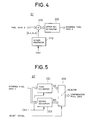
- Fig. 4 shows the internal structure of the dithering circuit 31 in the image data processor 3.
- N-bit pixel data D for each pixel corresponding to a video signal is sequentially supplied to an adder 320 for each first clock signal CK1 of a frequency fs as shown in Fig. 3. Since this video signal has been produced by interlaced scanning, pixel data corresponding to an odd row of pixels in the entire pixels of the PDP 10 shown in Fig. 2 are supplied first, and then pixel data corresponding to an even row of pixels are supplied. As shown in Fig. 3, for example, after pixel data D 11 -D 1m respectively corresponding to the first row of pixels G 11 -G 1m of Fig.
- pixel data D 31 -D 3m respectively corresponding to the next row or the third row of pixels G 31 -G 3m are supplied.
- pixel data Dml-Dmn respectively corresponding to the last odd row of pixels G n1 -G nm are supplied
- pixel data D 2l -D 2m respectively corresponding to the first even row of pixels G 21 -G 2m are supplied.
- a dither generator 310 repeatedly generates a dither coefficient a, dither coefficient c, dither coefficient b and dither coefficient d in circulation for each second clock signal CK2 of a frequency 2•fs as shown in Fig. 3, and supplies those dither coefficients to the adder 320.
- the adder 320 adds those dither coefficients to the pixel data D sequentially supplied from the A/D converter 1, and sends the resultant dither-added pixel data to an upper-bit extractor 330.
- the dither coefficient a is added to the pixel data D 11 at the first row and the first column to acquire dither-added pixel data (D 11 +a), and then the dither coefficient c is added to the pixel data D 11 to acquire dither-added pixel data (D 11 +c).
- the dither coefficient b is added to the pixel data D 12 at the first row and the second column to acquire dither-added pixel data (D 12 +b)
- the dither coefficient d is added to the pixel data D 12 to acquire dither-added pixel data (D 12 +d).
- two different dither coefficients are added to a single piece of pixel data to newly generate two pieces of dither-added pixel data.
- the upper-bit extractor 330 extracts upper M bits of data of such dither-added pixel data and supplies the data as dithered pixel data Z to the pseudo outline compensation data converter 32 at the subsequent stage.
- Fig. 5 shows the internal structure of the pseudo outline compensation data converter 32
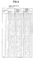
- a first converter 321 converts the dithered pixel data Z consisting of, for example, six bits supplied from the dithering circuit 31 to 8-bit pixel data based on a first mode conversion table as shown in Fig. 6 or 7, and supplies the converted data as pseudo outline compensation pixel data AZ to a selector 322.
- a second converter 323 converts the dithered pixel data Z consisting of, for example, six bits supplied from the dithering circuit 31 to 8-bit pixel data based on a second mode conversion table as shown in Fig. 6 or 7, and supplies the converted data as pseudo outline compensation pixel data BZ to the selector 322.
- the logic value "0" of each bit in the pseudo outline compensation pixel data AZ (BZ) shown in Fig. 6 or 7 designates no light emission while the logic value "1" designates light emission.
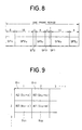
- the light emission period in one frame period accords to the light emission format in Fig. 8.
- bit 7 of the pseudo outline compensation pixel data AZ corresponds to light emission in the sub-frame SF4 in Fig. 8, and when its logic value is “1", light emission is carried out for the period of "8".
- Bit 6 corresponds to light emission in the sub-frame SF61, and when its logic value is “1”, light emission is carried out for the period of "16”.
- Bit 5 corresponds to light emission in the sub-frame SF2, and when its logic value is "1", light emission is carried out for the period of "2”.
- Bit 4 corresponds to light emission in the sub-frame SF5 1 , and when its logic value is "1", light emission is carried out for the period of "8".
- Bit 3 corresponds to light emission in the sub-frame SF3, and when its logic value is “1”, light emission is carried out for the period of "4".
- Bit 2 corresponds to light emission in the sub-frame SF1, and when its logic value is “1”, light emission is carried out for the period of "1”.
- Bit 1 corresponds to light emission in the sub-frame SF6 2 , and when its logic value is “1”, light emission is carried out for the period of "16”.
- bit 0 corresponds to light emission in the sub-frame SF52, and when its logic value is “1", light emission is carried out for the period of "8".
- the sum of the light emission periods in those SF1-SF6 is equivalent to the luminance level.
- the sub-frame SF6 (equivalent to the light emission period of "32") which has a heavy weight is separated to the sub-frames SF6 1 and SF6 2 each specifying the light emission period of "16" and both arranged apart from each other.
- the sub-frame SF5 (equivalent to the light emission period of "16") which also has a heavy weight is separated to the sub-frames SF5 1 and SF5 2 each specifying the light emission period of "8" and both arranged apart from each other.
- Two conversion patterns that have different light emission positions in sub-frames in one frame, whose total light emission periods are the same and whose light emission periods are equal to one another, are prepared in the first and second mode conversion tables to suppress a pseudo outline.
- a pseudo outline can be suppressed by shifting the position of light emission in one frame period from one pixel to another adjacent pixel in the aforementioned manner.
- Driving for such light emission is carried out by the row electrode driver 5 and the column electrode driver 6.
- Data conversions by the first converter 321 and the second converter 323 are executed in synchronism with the second clock signal CK2.
- the selector 322 selects one of the pseudo outline compensation pixel data AZ supplied from the first converter 321 and the pseudo outline compensation pixel data BZ supplied from the second converter 323 which accords to the logic value of a select signal supplied from the control circuit 2 as shown in Fig. 3, and sends the selected one to the frame memory 4.
- the selector 322 selects the pseudo outline compensation pixel data AZ supplied from the first converter 321 and sends it to the frame memory 4.
- the selector 322 selects the pseudo outline compensation pixel data BZ supplied from the second converter 323 and sends it to the frame memory 4.
- the operations of the dithering circuit 31 and the pseudo outline compensation data converter 32 permit the first compensation pixel data AZ(D 11 +a) and the second compensation pixel data BZ(D 11 +c) to be generated based on the pixel data D 11 supplied in association with the pixel G 11 in Fig. 2 and to be stored in the frame memory 4. Further, the first compensation pixel data BZ(D 12 +b) and the second compensation pixel data AZ(D 12 +d) are generated based on the pixel data D 12 associated with the pixel G 12 in Fig. 2 and are stored in the frame memory 4.
- the first compensation pixel data AZ(D 11 +a) is read out from the frame memory 4 as pixel drive data corresponding to the pixel G 11 at the first row and first column
- the first compensation pixel data BZ(D 12 +b) is read out from the frame memory 4 as pixel drive data corresponding to the pixel G 12 at the first row and second column.
- the second compensation pixel data BZ(D 11 +c) is read out from the frame memory 4 as pixel drive data corresponding to the pixel G 21 at the second row and first column
- the second compensation pixel data AZ(D 12 +d) is read out from the frame memory 4 as pixel drive data corresponding to the pixel G 22 at the second row and second column.
- the first compensation pixel data AZ(D 11 +a) and BZ(D 12 +b) are image-processed pixel data which is the supplied pixel data corresponding to the first row having undergone image processing by the image data processor 3.
- the second compensation pixel data BZ(D 11 +c) and AZ(D 12 +d) are compensation pixel data corresponding to the second row interpolated on the basis of the first row of pixel data.
- Pixel drive data respectively corresponding to those image-processed pixel data and interpolation pixel data are sequentially read from the frame memory 4 from the one that corresponds to the first row, and are supplied to the column electrode driver 6. This operation permits display in an linear scanning mode to be effected based on the video signal produced by the interlaced scanning.
- the drive apparatus embodying this invention as apparent from the above, two different image processes are performed on pixel data obtained by sampling interlaced scanning originated video signal, yielding image-processed pixel data and interpolation pixel data.
- the self light-emitting display unit is driven in an linear scanning mode by treating the image-processed pixel data as pixel drive data associated with one of an odd line and an even line of the self light-emitting display unit and treating the interpolation pixel data as pixel drive data associated with the other one of the odd line and even line.
- this invention is effective in that at the time a video signal of a interlaced scanning mode is converted to a video signal of an linear scanning mode which is to be displayed, noise and dot interference on the screen, which are originated from image processing, are suppressed, advantageously.
Landscapes
- Engineering & Computer Science (AREA)
- Physics & Mathematics (AREA)
- Computer Hardware Design (AREA)
- General Physics & Mathematics (AREA)
- Theoretical Computer Science (AREA)
- Plasma & Fusion (AREA)
- Control Of Indicators Other Than Cathode Ray Tubes (AREA)
- Control Of Gas Discharge Display Tubes (AREA)
- Transforming Electric Information Into Light Information (AREA)
Applications Claiming Priority (2)
| Application Number | Priority Date | Filing Date | Title |
|---|---|---|---|
| JP249634/96 | 1996-09-20 | ||
| JP8249634A JPH1098662A (ja) | 1996-09-20 | 1996-09-20 | 自発光表示器の駆動装置 |
Publications (2)
| Publication Number | Publication Date |
|---|---|
| EP0831449A2 true EP0831449A2 (fr) | 1998-03-25 |
| EP0831449A3 EP0831449A3 (fr) | 1998-04-22 |
Family
ID=17195948
Family Applications (1)
| Application Number | Title | Priority Date | Filing Date |
|---|---|---|---|
| EP97305309A Withdrawn EP0831449A3 (fr) | 1996-09-20 | 1997-07-16 | Appareil de commande pour un dispositif d'affichage luminescent |
Country Status (3)
| Country | Link |
|---|---|
| US (1) | US6008793A (fr) |
| EP (1) | EP0831449A3 (fr) |
| JP (1) | JPH1098662A (fr) |
Cited By (9)
| Publication number | Priority date | Publication date | Assignee | Title |
|---|---|---|---|---|
| EP1022714A3 (fr) * | 1999-01-18 | 2001-05-09 | Pioneer Corporation | Méthode de commande pour un panneau d'affichage à plasma |
| EP1184833A2 (fr) * | 2000-09-04 | 2002-03-06 | Sel Semiconductor Energy Laboratory Co., Ltd. | Méthode de commande d'un dispositif d'affichage électroluminescent |
| US7283111B2 (en) | 2001-08-03 | 2007-10-16 | Semiconductor Energy Laboratory Co., Ltd. | Display device and method of driving thereof |
| US7502040B2 (en) | 2004-12-06 | 2009-03-10 | Semiconductor Energy Laboratory Co., Ltd. | Display device, driving method thereof and electronic appliance |
| US7623091B2 (en) | 2005-05-02 | 2009-11-24 | Semiconductor Energy Laboratory Co., Ltd. | Display device, and driving method and electronic apparatus of the display device |
| US7719526B2 (en) | 2005-04-14 | 2010-05-18 | Semiconductor Energy Laboratory Co., Ltd. | Display device, and driving method and electronic apparatus of the display device |
| US7755651B2 (en) | 2006-01-20 | 2010-07-13 | Semiconductor Energy Laboratory Co., Ltd. | Driving method of display device |
| US8378935B2 (en) | 2005-01-14 | 2013-02-19 | Semiconductor Energy Laboratory Co., Ltd. | Display device having a plurality of subframes and method of driving the same |
| US8633919B2 (en) | 2005-04-14 | 2014-01-21 | Semiconductor Energy Laboratory Co., Ltd. | Display device, driving method of the display device, and electronic device |
Families Citing this family (17)
| Publication number | Priority date | Publication date | Assignee | Title |
|---|---|---|---|---|
| JP2994633B2 (ja) * | 1997-12-10 | 1999-12-27 | 松下電器産業株式会社 | 疑似輪郭ノイズ検出装置およびそれを用いた表示装置 |
| US6417825B1 (en) * | 1998-09-29 | 2002-07-09 | Sarnoff Corporation | Analog active matrix emissive display |
| EP0994457B1 (fr) * | 1998-10-12 | 2007-09-05 | Victor Company Of Japan, Limited | Appareil et méthode de traitement d'échelle des gris de signal vidéo pour un appareil d'affichage matriciel |
| EP1049068A1 (fr) * | 1999-04-28 | 2000-11-02 | THOMSON multimedia S.A. | Procédé et dispositif pour traitement de signaux vidéo |
| JP3720275B2 (ja) * | 2001-04-16 | 2005-11-24 | シャープ株式会社 | 画像表示パネル、画像表示装置、並びに画像表示方法 |
| JP2002351381A (ja) * | 2001-05-30 | 2002-12-06 | Pioneer Electronic Corp | ディスプレイ装置及びディスプレイパネルの駆動方法 |
| US6963319B2 (en) * | 2002-08-07 | 2005-11-08 | Hewlett-Packard Development Company, L.P. | Image display system and method |
| US8289233B1 (en) | 2003-02-04 | 2012-10-16 | Imaging Systems Technology | Error diffusion |
| US8305301B1 (en) | 2003-02-04 | 2012-11-06 | Imaging Systems Technology | Gamma correction |
| JP4410997B2 (ja) | 2003-02-20 | 2010-02-10 | パナソニック株式会社 | 表示パネルの駆動装置 |
| US7391391B2 (en) * | 2003-11-13 | 2008-06-24 | Victor Company Of Japan, Limited | Display apparatus |
| WO2006013799A1 (fr) * | 2004-08-03 | 2006-02-09 | Semiconductor Energy Laboratory Co., Ltd. | Dispositif d'affichage et procede d'attaque |
| ATE488835T1 (de) | 2005-12-22 | 2010-12-15 | Imaging Systems Technology Inc | Sas-adressierung einer ac-plasmaanzeige mit oberflächenentladung |
| WO2007113275A1 (fr) * | 2006-04-03 | 2007-10-11 | Thomson Licensing | Procédé et dispositif de codage de niveaux vidéo dans un panneau d'affichage plasma |
| US8248328B1 (en) | 2007-05-10 | 2012-08-21 | Imaging Systems Technology | Plasma-shell PDP with artifact reduction |
| KR20150019686A (ko) * | 2013-08-14 | 2015-02-25 | 삼성디스플레이 주식회사 | 룩업 테이블에 기반한 부분적 의사 윤관 검출 방법 및 그 장치, 그리고 이를 이용한 영상 데이터 보정 방법 |
| US11282434B1 (en) * | 2020-12-29 | 2022-03-22 | Solomon Systech (China) Limited | Driving method for active matrix display |
Family Cites Families (17)
| Publication number | Priority date | Publication date | Assignee | Title |
|---|---|---|---|---|
| US4720745A (en) * | 1983-06-22 | 1988-01-19 | Digivision, Inc. | Method and apparatus for enhancing video displays |
| US4956638A (en) * | 1988-09-16 | 1990-09-11 | International Business Machines Corporation | Display using ordered dither |
| JP2738865B2 (ja) * | 1989-06-30 | 1998-04-08 | キヤノン株式会社 | 画像処理装置 |
| US5093721A (en) * | 1990-07-10 | 1992-03-03 | Zenith Electronics Corporation | Line interpolator with preservation of diagonal resolution |
| US5159451A (en) * | 1991-03-19 | 1992-10-27 | Faroudja Y C | Field memory expansible line doubler for television receiver |
| TW232060B (en) * | 1992-10-06 | 1994-10-11 | Seiko Epson Corp | Image processing apparatus |
| JPH06282242A (ja) * | 1993-03-25 | 1994-10-07 | Pioneer Electron Corp | ガス放電パネルの駆動方法 |
| EP0624032B1 (fr) * | 1993-05-07 | 2000-07-26 | Lg Electronics Inc. | Procédé et appareil de conversion de format vidéo |
| JPH07140926A (ja) * | 1993-11-17 | 1995-06-02 | Fujitsu Ltd | フラットディスプレイ装置の走査制御方法 |
| JP3333839B2 (ja) * | 1994-04-19 | 2002-10-15 | 松下電器産業株式会社 | 補間ライン検出方法及び補間ライン検出装置 |
| JP2760295B2 (ja) * | 1994-10-06 | 1998-05-28 | 株式会社富士通ゼネラル | ディスプレイ装置の誤差拡散処理装置 |
| US5886745A (en) * | 1994-12-09 | 1999-03-23 | Matsushita Electric Industrial Co., Ltd. | Progressive scanning conversion apparatus |
| DE69609471T2 (de) * | 1995-05-12 | 2001-03-29 | Koninkl Philips Electronics Nv | Bildanzeigevorrichtung mit zeilenzahlumwandlung |
| US5714975A (en) * | 1995-05-31 | 1998-02-03 | Canon Kabushiki Kaisha | Apparatus and method for generating halftoning or dither values |
| US5784116A (en) * | 1995-06-29 | 1998-07-21 | Motorola Inc. | Method of generating high-resolution video |
| US5532751A (en) * | 1995-07-31 | 1996-07-02 | Lui; Sam | Edge-based interlaced to progressive video conversion system |
| US5818419A (en) * | 1995-10-31 | 1998-10-06 | Fujitsu Limited | Display device and method for driving the same |
-
1996
- 1996-09-20 JP JP8249634A patent/JPH1098662A/ja active Pending
-
1997
- 1997-07-11 US US08/890,752 patent/US6008793A/en not_active Expired - Lifetime
- 1997-07-16 EP EP97305309A patent/EP0831449A3/fr not_active Withdrawn
Cited By (17)
| Publication number | Priority date | Publication date | Assignee | Title |
|---|---|---|---|---|
| US6646625B1 (en) | 1999-01-18 | 2003-11-11 | Pioneer Corporation | Method for driving a plasma display panel |
| US6967636B2 (en) | 1999-01-18 | 2005-11-22 | Pioneer Corporation | Method for driving a plasma display panel |
| US7042424B2 (en) | 1999-01-18 | 2006-05-09 | Pioneer Corporation | Method for driving a plasma display panel |
| EP1022714A3 (fr) * | 1999-01-18 | 2001-05-09 | Pioneer Corporation | Méthode de commande pour un panneau d'affichage à plasma |
| EP1970884A3 (fr) * | 2000-09-04 | 2008-09-24 | Semiconductor Energy Laboratory Co., Ltd. | Procédé d'afficheur à électroluminescence et afficheur à électroluminescence |
| EP1184833A2 (fr) * | 2000-09-04 | 2002-03-06 | Sel Semiconductor Energy Laboratory Co., Ltd. | Méthode de commande d'un dispositif d'affichage électroluminescent |
| US7106290B2 (en) | 2000-09-04 | 2006-09-12 | Semiconductor Energy Laboratory Co., Ltd. | Method of driving EL display device |
| US8373625B2 (en) | 2001-08-03 | 2013-02-12 | Semiconductor Energy Laboratory Co., Ltd. | Display device and method of driving thereof |
| US7283111B2 (en) | 2001-08-03 | 2007-10-16 | Semiconductor Energy Laboratory Co., Ltd. | Display device and method of driving thereof |
| US7502040B2 (en) | 2004-12-06 | 2009-03-10 | Semiconductor Energy Laboratory Co., Ltd. | Display device, driving method thereof and electronic appliance |
| US8378935B2 (en) | 2005-01-14 | 2013-02-19 | Semiconductor Energy Laboratory Co., Ltd. | Display device having a plurality of subframes and method of driving the same |
| US7719526B2 (en) | 2005-04-14 | 2010-05-18 | Semiconductor Energy Laboratory Co., Ltd. | Display device, and driving method and electronic apparatus of the display device |
| US8633919B2 (en) | 2005-04-14 | 2014-01-21 | Semiconductor Energy Laboratory Co., Ltd. | Display device, driving method of the display device, and electronic device |
| US9047809B2 (en) | 2005-04-14 | 2015-06-02 | Semiconductor Energy Laboratory Co., Ltd. | Display device and driving method and electronic apparatus of the display device |
| US7623091B2 (en) | 2005-05-02 | 2009-11-24 | Semiconductor Energy Laboratory Co., Ltd. | Display device, and driving method and electronic apparatus of the display device |
| US7755651B2 (en) | 2006-01-20 | 2010-07-13 | Semiconductor Energy Laboratory Co., Ltd. | Driving method of display device |
| US8659520B2 (en) | 2006-01-20 | 2014-02-25 | Semiconductor Energy Laboratory Co., Ltd. | Driving method of display device |
Also Published As
| Publication number | Publication date |
|---|---|
| US6008793A (en) | 1999-12-28 |
| EP0831449A3 (fr) | 1998-04-22 |
| JPH1098662A (ja) | 1998-04-14 |
Similar Documents
| Publication | Publication Date | Title |
|---|---|---|
| US6008793A (en) | Drive apparatus for self light emitting display unit | |
| EP0831450B1 (fr) | Appareil de commande pour un dispositif d'affichage luminescent | |
| JP3750889B2 (ja) | ディスプレイパネルの中間調表示方法 | |
| KR100478378B1 (ko) | 표시 장치 및 표시 방법 | |
| US6462721B2 (en) | PDP display drive pulse controller for preventing light emission center fluctuation | |
| JP3489884B2 (ja) | フレーム内時分割型表示装置及びフレーム内時分割型表示装置における中間調表示方法 | |
| KR100467447B1 (ko) | 플라즈마 디스플레이 패널의 화상 표시 방법 및 그 장치 | |
| EP0833299A1 (fr) | Procédé d'expression d'échelle de gris et dispositif d'affichage d'échelle de gris | |
| EP1022714A2 (fr) | Méthode de commande pour un panneau d'affichage à plasma | |
| JPH1124628A (ja) | プラズマディスプレイパネルの階調表示方法 | |
| JPH10124000A (ja) | 自発光表示器の駆動装置 | |
| JPH09218662A (ja) | 自発光画像表示パネルの駆動方法 | |
| EP1262943A2 (fr) | Panneau d'affichage à plasma et son procédé de commande | |
| JP2002351390A (ja) | 表示装置及び階調表示方法 | |
| JP3336935B2 (ja) | 画像表示装置 | |
| JP4731841B2 (ja) | 表示パネルの駆動装置及び駆動方法 | |
| KR100446760B1 (ko) | 계조표시 방법 및 표시장치 | |
| JP3656995B2 (ja) | 画像表示方法及び画像表示装置 | |
| JP2002366085A (ja) | 表示装置及び階調表示処理方法 | |
| JP2006065269A (ja) | ディスプレイ装置及びその駆動方法 | |
| KR100346809B1 (ko) | 중간조 표시 방법 및 표시 장치 | |
| JP3365614B2 (ja) | プラズマディスプレイパネル表示装置及びその駆動方法 | |
| JP2001255846A (ja) | プラズマディスプレイパネルの階調表示処理装置 | |
| JP2001249640A (ja) | プラズマディスプレイパネルの駆動方法 | |
| JP2003015589A (ja) | 表示装置及び階調表示方法 |
Legal Events
| Date | Code | Title | Description |
|---|---|---|---|
| PUAI | Public reference made under article 153(3) epc to a published international application that has entered the european phase |
Free format text: ORIGINAL CODE: 0009012 |
|
| PUAL | Search report despatched |
Free format text: ORIGINAL CODE: 0009013 |
|
| AK | Designated contracting states |
Kind code of ref document: A2 Designated state(s): DE FR GB |
|
| AX | Request for extension of the european patent |
Free format text: AL;LT;LV;RO;SI |
|
| AK | Designated contracting states |
Kind code of ref document: A3 Designated state(s): AT BE CH DE DK ES FI FR GB GR IE IT LI LU MC NL PT SE |
|
| AX | Request for extension of the european patent |
Free format text: AL;LT;LV;RO;SI |
|
| 17P | Request for examination filed |
Effective date: 19980416 |
|
| AKX | Designation fees paid |
Free format text: DE FR GB |
|
| RBV | Designated contracting states (corrected) |
Designated state(s): DE FR GB |
|
| STAA | Information on the status of an ep patent application or granted ep patent |
Free format text: STATUS: THE APPLICATION IS DEEMED TO BE WITHDRAWN |
|
| 18D | Application deemed to be withdrawn |
Effective date: 20030202 |