EP1262943A2 - Panneau d'affichage à plasma et son procédé de commande - Google Patents
Panneau d'affichage à plasma et son procédé de commande Download PDFInfo
- Publication number
- EP1262943A2 EP1262943A2 EP02010751A EP02010751A EP1262943A2 EP 1262943 A2 EP1262943 A2 EP 1262943A2 EP 02010751 A EP02010751 A EP 02010751A EP 02010751 A EP02010751 A EP 02010751A EP 1262943 A2 EP1262943 A2 EP 1262943A2
- Authority
- EP
- European Patent Office
- Prior art keywords
- dither
- column
- display
- display cells
- pixel data
- Prior art date
- Legal status (The legal status is an assumption and is not a legal conclusion. Google has not performed a legal analysis and makes no representation as to the accuracy of the status listed.)
- Withdrawn
Links
- 238000000034 method Methods 0.000 title claims description 7
- 239000011159 matrix material Substances 0.000 claims description 54
- 239000003086 colorant Substances 0.000 claims description 6
- 230000004044 response Effects 0.000 claims description 6
- 238000006243 chemical reaction Methods 0.000 description 28
- 230000008030 elimination Effects 0.000 description 16
- 238000003379 elimination reaction Methods 0.000 description 16
- 238000009792 diffusion process Methods 0.000 description 13
- 241001270131 Agaricus moelleri Species 0.000 description 9
- 238000001514 detection method Methods 0.000 description 7
- 239000000284 extract Substances 0.000 description 7
- 238000000605 extraction Methods 0.000 description 7
- 238000000926 separation method Methods 0.000 description 7
- 230000007704 transition Effects 0.000 description 6
- 238000010586 diagram Methods 0.000 description 3
- 230000008033 biological extinction Effects 0.000 description 1
- 230000006835 compression Effects 0.000 description 1
- 238000007906 compression Methods 0.000 description 1
- 230000002093 peripheral effect Effects 0.000 description 1
- 230000002459 sustained effect Effects 0.000 description 1
- 230000001360 synchronised effect Effects 0.000 description 1
Images





Classifications
-
- G—PHYSICS
- G09—EDUCATION; CRYPTOGRAPHY; DISPLAY; ADVERTISING; SEALS
- G09G—ARRANGEMENTS OR CIRCUITS FOR CONTROL OF INDICATING DEVICES USING STATIC MEANS TO PRESENT VARIABLE INFORMATION
- G09G3/00—Control arrangements or circuits, of interest only in connection with visual indicators other than cathode-ray tubes
- G09G3/20—Control arrangements or circuits, of interest only in connection with visual indicators other than cathode-ray tubes for presentation of an assembly of a number of characters, e.g. a page, by composing the assembly by combination of individual elements arranged in a matrix no fixed position being assigned to or needed to be assigned to the individual characters or partial characters
- G09G3/2007—Display of intermediate tones
- G09G3/2059—Display of intermediate tones using error diffusion
-
- G—PHYSICS
- G09—EDUCATION; CRYPTOGRAPHY; DISPLAY; ADVERTISING; SEALS
- G09G—ARRANGEMENTS OR CIRCUITS FOR CONTROL OF INDICATING DEVICES USING STATIC MEANS TO PRESENT VARIABLE INFORMATION
- G09G3/00—Control arrangements or circuits, of interest only in connection with visual indicators other than cathode-ray tubes
- G09G3/20—Control arrangements or circuits, of interest only in connection with visual indicators other than cathode-ray tubes for presentation of an assembly of a number of characters, e.g. a page, by composing the assembly by combination of individual elements arranged in a matrix no fixed position being assigned to or needed to be assigned to the individual characters or partial characters
- G09G3/2007—Display of intermediate tones
- G09G3/2018—Display of intermediate tones by time modulation using two or more time intervals
- G09G3/2022—Display of intermediate tones by time modulation using two or more time intervals using sub-frames
-
- G—PHYSICS
- G09—EDUCATION; CRYPTOGRAPHY; DISPLAY; ADVERTISING; SEALS
- G09G—ARRANGEMENTS OR CIRCUITS FOR CONTROL OF INDICATING DEVICES USING STATIC MEANS TO PRESENT VARIABLE INFORMATION
- G09G3/00—Control arrangements or circuits, of interest only in connection with visual indicators other than cathode-ray tubes
- G09G3/20—Control arrangements or circuits, of interest only in connection with visual indicators other than cathode-ray tubes for presentation of an assembly of a number of characters, e.g. a page, by composing the assembly by combination of individual elements arranged in a matrix no fixed position being assigned to or needed to be assigned to the individual characters or partial characters
- G09G3/2007—Display of intermediate tones
- G09G3/2044—Display of intermediate tones using dithering
- G09G3/2051—Display of intermediate tones using dithering with use of a spatial dither pattern
- G09G3/2055—Display of intermediate tones using dithering with use of a spatial dither pattern the pattern being varied in time
-
- G—PHYSICS
- G09—EDUCATION; CRYPTOGRAPHY; DISPLAY; ADVERTISING; SEALS
- G09G—ARRANGEMENTS OR CIRCUITS FOR CONTROL OF INDICATING DEVICES USING STATIC MEANS TO PRESENT VARIABLE INFORMATION
- G09G3/00—Control arrangements or circuits, of interest only in connection with visual indicators other than cathode-ray tubes
- G09G3/20—Control arrangements or circuits, of interest only in connection with visual indicators other than cathode-ray tubes for presentation of an assembly of a number of characters, e.g. a page, by composing the assembly by combination of individual elements arranged in a matrix no fixed position being assigned to or needed to be assigned to the individual characters or partial characters
- G09G3/2007—Display of intermediate tones
- G09G3/2077—Display of intermediate tones by a combination of two or more gradation control methods
-
- G—PHYSICS
- G09—EDUCATION; CRYPTOGRAPHY; DISPLAY; ADVERTISING; SEALS
- G09G—ARRANGEMENTS OR CIRCUITS FOR CONTROL OF INDICATING DEVICES USING STATIC MEANS TO PRESENT VARIABLE INFORMATION
- G09G3/00—Control arrangements or circuits, of interest only in connection with visual indicators other than cathode-ray tubes
- G09G3/20—Control arrangements or circuits, of interest only in connection with visual indicators other than cathode-ray tubes for presentation of an assembly of a number of characters, e.g. a page, by composing the assembly by combination of individual elements arranged in a matrix no fixed position being assigned to or needed to be assigned to the individual characters or partial characters
- G09G3/22—Control arrangements or circuits, of interest only in connection with visual indicators other than cathode-ray tubes for presentation of an assembly of a number of characters, e.g. a page, by composing the assembly by combination of individual elements arranged in a matrix no fixed position being assigned to or needed to be assigned to the individual characters or partial characters using controlled light sources
- G09G3/28—Control arrangements or circuits, of interest only in connection with visual indicators other than cathode-ray tubes for presentation of an assembly of a number of characters, e.g. a page, by composing the assembly by combination of individual elements arranged in a matrix no fixed position being assigned to or needed to be assigned to the individual characters or partial characters using controlled light sources using luminous gas-discharge panels, e.g. plasma panels
- G09G3/288—Control arrangements or circuits, of interest only in connection with visual indicators other than cathode-ray tubes for presentation of an assembly of a number of characters, e.g. a page, by composing the assembly by combination of individual elements arranged in a matrix no fixed position being assigned to or needed to be assigned to the individual characters or partial characters using controlled light sources using luminous gas-discharge panels, e.g. plasma panels using AC panels
- G09G3/291—Control arrangements or circuits, of interest only in connection with visual indicators other than cathode-ray tubes for presentation of an assembly of a number of characters, e.g. a page, by composing the assembly by combination of individual elements arranged in a matrix no fixed position being assigned to or needed to be assigned to the individual characters or partial characters using controlled light sources using luminous gas-discharge panels, e.g. plasma panels using AC panels controlling the gas discharge to control a cell condition, e.g. by means of specific pulse shapes
- G09G3/292—Control arrangements or circuits, of interest only in connection with visual indicators other than cathode-ray tubes for presentation of an assembly of a number of characters, e.g. a page, by composing the assembly by combination of individual elements arranged in a matrix no fixed position being assigned to or needed to be assigned to the individual characters or partial characters using controlled light sources using luminous gas-discharge panels, e.g. plasma panels using AC panels controlling the gas discharge to control a cell condition, e.g. by means of specific pulse shapes for reset discharge, priming discharge or erase discharge occurring in a phase other than addressing
- G09G3/2927—Details of initialising
-
- G—PHYSICS
- G09—EDUCATION; CRYPTOGRAPHY; DISPLAY; ADVERTISING; SEALS
- G09G—ARRANGEMENTS OR CIRCUITS FOR CONTROL OF INDICATING DEVICES USING STATIC MEANS TO PRESENT VARIABLE INFORMATION
- G09G3/00—Control arrangements or circuits, of interest only in connection with visual indicators other than cathode-ray tubes
- G09G3/20—Control arrangements or circuits, of interest only in connection with visual indicators other than cathode-ray tubes for presentation of an assembly of a number of characters, e.g. a page, by composing the assembly by combination of individual elements arranged in a matrix no fixed position being assigned to or needed to be assigned to the individual characters or partial characters
- G09G3/22—Control arrangements or circuits, of interest only in connection with visual indicators other than cathode-ray tubes for presentation of an assembly of a number of characters, e.g. a page, by composing the assembly by combination of individual elements arranged in a matrix no fixed position being assigned to or needed to be assigned to the individual characters or partial characters using controlled light sources
- G09G3/28—Control arrangements or circuits, of interest only in connection with visual indicators other than cathode-ray tubes for presentation of an assembly of a number of characters, e.g. a page, by composing the assembly by combination of individual elements arranged in a matrix no fixed position being assigned to or needed to be assigned to the individual characters or partial characters using controlled light sources using luminous gas-discharge panels, e.g. plasma panels
- G09G3/288—Control arrangements or circuits, of interest only in connection with visual indicators other than cathode-ray tubes for presentation of an assembly of a number of characters, e.g. a page, by composing the assembly by combination of individual elements arranged in a matrix no fixed position being assigned to or needed to be assigned to the individual characters or partial characters using controlled light sources using luminous gas-discharge panels, e.g. plasma panels using AC panels
- G09G3/291—Control arrangements or circuits, of interest only in connection with visual indicators other than cathode-ray tubes for presentation of an assembly of a number of characters, e.g. a page, by composing the assembly by combination of individual elements arranged in a matrix no fixed position being assigned to or needed to be assigned to the individual characters or partial characters using controlled light sources using luminous gas-discharge panels, e.g. plasma panels using AC panels controlling the gas discharge to control a cell condition, e.g. by means of specific pulse shapes
- G09G3/293—Control arrangements or circuits, of interest only in connection with visual indicators other than cathode-ray tubes for presentation of an assembly of a number of characters, e.g. a page, by composing the assembly by combination of individual elements arranged in a matrix no fixed position being assigned to or needed to be assigned to the individual characters or partial characters using controlled light sources using luminous gas-discharge panels, e.g. plasma panels using AC panels controlling the gas discharge to control a cell condition, e.g. by means of specific pulse shapes for address discharge
- G09G3/2935—Addressed by erasing selected cells that are in an ON state
-
- G—PHYSICS
- G09—EDUCATION; CRYPTOGRAPHY; DISPLAY; ADVERTISING; SEALS
- G09G—ARRANGEMENTS OR CIRCUITS FOR CONTROL OF INDICATING DEVICES USING STATIC MEANS TO PRESENT VARIABLE INFORMATION
- G09G3/00—Control arrangements or circuits, of interest only in connection with visual indicators other than cathode-ray tubes
- G09G3/20—Control arrangements or circuits, of interest only in connection with visual indicators other than cathode-ray tubes for presentation of an assembly of a number of characters, e.g. a page, by composing the assembly by combination of individual elements arranged in a matrix no fixed position being assigned to or needed to be assigned to the individual characters or partial characters
- G09G3/22—Control arrangements or circuits, of interest only in connection with visual indicators other than cathode-ray tubes for presentation of an assembly of a number of characters, e.g. a page, by composing the assembly by combination of individual elements arranged in a matrix no fixed position being assigned to or needed to be assigned to the individual characters or partial characters using controlled light sources
- G09G3/28—Control arrangements or circuits, of interest only in connection with visual indicators other than cathode-ray tubes for presentation of an assembly of a number of characters, e.g. a page, by composing the assembly by combination of individual elements arranged in a matrix no fixed position being assigned to or needed to be assigned to the individual characters or partial characters using controlled light sources using luminous gas-discharge panels, e.g. plasma panels
- G09G3/288—Control arrangements or circuits, of interest only in connection with visual indicators other than cathode-ray tubes for presentation of an assembly of a number of characters, e.g. a page, by composing the assembly by combination of individual elements arranged in a matrix no fixed position being assigned to or needed to be assigned to the individual characters or partial characters using controlled light sources using luminous gas-discharge panels, e.g. plasma panels using AC panels
- G09G3/291—Control arrangements or circuits, of interest only in connection with visual indicators other than cathode-ray tubes for presentation of an assembly of a number of characters, e.g. a page, by composing the assembly by combination of individual elements arranged in a matrix no fixed position being assigned to or needed to be assigned to the individual characters or partial characters using controlled light sources using luminous gas-discharge panels, e.g. plasma panels using AC panels controlling the gas discharge to control a cell condition, e.g. by means of specific pulse shapes
- G09G3/293—Control arrangements or circuits, of interest only in connection with visual indicators other than cathode-ray tubes for presentation of an assembly of a number of characters, e.g. a page, by composing the assembly by combination of individual elements arranged in a matrix no fixed position being assigned to or needed to be assigned to the individual characters or partial characters using controlled light sources using luminous gas-discharge panels, e.g. plasma panels using AC panels controlling the gas discharge to control a cell condition, e.g. by means of specific pulse shapes for address discharge
- G09G3/2937—Control arrangements or circuits, of interest only in connection with visual indicators other than cathode-ray tubes for presentation of an assembly of a number of characters, e.g. a page, by composing the assembly by combination of individual elements arranged in a matrix no fixed position being assigned to or needed to be assigned to the individual characters or partial characters using controlled light sources using luminous gas-discharge panels, e.g. plasma panels using AC panels controlling the gas discharge to control a cell condition, e.g. by means of specific pulse shapes for address discharge being addressed only once per frame
-
- G—PHYSICS
- G09—EDUCATION; CRYPTOGRAPHY; DISPLAY; ADVERTISING; SEALS
- G09G—ARRANGEMENTS OR CIRCUITS FOR CONTROL OF INDICATING DEVICES USING STATIC MEANS TO PRESENT VARIABLE INFORMATION
- G09G3/00—Control arrangements or circuits, of interest only in connection with visual indicators other than cathode-ray tubes
- G09G3/20—Control arrangements or circuits, of interest only in connection with visual indicators other than cathode-ray tubes for presentation of an assembly of a number of characters, e.g. a page, by composing the assembly by combination of individual elements arranged in a matrix no fixed position being assigned to or needed to be assigned to the individual characters or partial characters
- G09G3/2003—Display of colours
Definitions
- This invention relates to a display device having display cells arranged in a matrix.
- PDPs plasma display panels
- a plurality of discharge cells serving as pixels are arranged in a matrix
- PDPs are directly driven by digital image signals, and the number of brightness grayscales which can be represented is determined by the number of bits of pixel data for each pixel, based on the above digital image signal.
- the subfield method in which the display period of one field is divided into a plurality of subfields for driving, is known as one method of PDP grayscale driving. For example, when there are 8 bits of pixel data, the display period of one field is divided, into eight subfields, SF8, SF7, ..., SF1, in order of weighting.
- Each subfield includes an address period, which sets the lit pixel state or the extinguished pixel state for each pixel according to the pixel data, and an emission sustain period which causes only pixels in the above lit pixel state to emit for a period corresponding to the weighting for that subfield.
- discharge cells are set to either light or not light within that subfield (the address period), and only those discharge cells set in the lit state are caused to emit for the period allocated for that subfield (emission sustain period).
- the number of perceived grayscales can be increased and image quality improved by employing dither processing in such grayscale driving.
- dither processing for example, four neighboring pixels above and below, and left and right, are treated as one set, and four dither coefficients consisting of different coefficient values (for example, 0, 1, 2, 3) are added to the four pixel data corresponding to the four pixels of this set respectively.
- dither processing increases the apparent number of grayscales.
- An object of the present invention is to provide a display device capable of presenting good-quality image display in which dither patterns are suppressed.
- a display device for displaying an image, in response to an image (video) signal, on a display screen, in which display screen each of pixels includes a plurality of display cells with different emission colors and the pixels are arranged in a matrix
- the display device comprising: means for converting the image signal into the pixel data such that each of the pixel data corresponds to each of the display cells; dither coefficient generation means for generating dither coefficients such that each of the dither coefficients corresponds to each of the display cells within the pixel; addition means for adding the dither coefficients to the pixel data to obtain dither-added pixel data; and display driving means for causing emission of the display cells in accordance with the dither-added pixel data.
- a value of the dither coefficient corresponding to a display cell used for emission of (at least) one color within the pixel is set to be different from values of other dither coefficients corresponding to other display cells used for emission of other colors within the pixel.
- the dither coefficients added to the pixel data to drive display cells responsible for at least one display color are different in value from the dither coefficients added to the pixel data to drive display cells responsible for another display color. Hence a specific dither pattern is no longer visually recognized in a screen. Consequently good-quality image display is obtained, with the occurrence of dither patterns suppressed.
- FIG. 1 a configuration of a display device of one embodiment of the present invention is illustrated.
- the display device shown in Fig. 1 is a plasma display device equipped with a plasma display panel as a display device.
- This display device includes a PDP 10 as the plasma display panel, and a driving unit.
- the drive unit includes synchronization detection circuit 1, driving control circuit 2, A/D converter 4, data conversion circuit 30, memory 5, address driver 6, first sustaining driver 7, and second sustaining driver 8.
- the PDP 10 includes column electrodes D 1 to D m as address electrodes, and row electrodes X 1 to X n and row electrodes Y 1 to Y n arranged perpendicularly to the column electrodes.
- row electrodes corresponding to one display line worth is formed from a pair of the row electrode X and row electrode Y.
- Column electrodes D 1 to D m are divided into column electrodes D 1 , D 4 , D 7 , ..., D m-2 , which handle red emission;
- column electrodes D 2 , D 5 , D 8 , ..., D m-1 which handle green emission; and
- Red discharge cells which emit red light on discharge are formed at each of the intersections of the column electrodes D 1 , D 4 , D 7 , ..., D m-2 , which handle red emission, and the row electrodes X and Y.
- Green discharge cells which emit green light on discharge are formed at each of the intersections of the column electrodes D 2 , D 5 , D 8 , ..., D m-1 , which handle green emission, and the row electrodes X and Y.
- Blue discharge cells which emit blue light on discharge are formed at each of the intersections of the column electrodes D 3 , D 6 , D 9 , ..., D m , which handle blue emission, and the row electrodes X and Y.
- one pixel is formed from three discharge cells neighboring in the display line direction, that is, from a red discharge cell, green discharge cell, and blue discharge cell.
- the synchronization detection circuit 1 generates a vertical sync signal V when a vertical sync signal is detected in the analog image signal. Also, the synchronization detection circuit 1 generates a horizontal sync signal H when a horizontal sync signal is detected in the image signal. The synchronization detection circuit 1 supplies these vertical sync signals V and horizontal sync signals H to the driving control circuit 2 and data conversion circuit 30.
- the A/D converter 4 samples the image signal in response to a clock signal supplied by the driving control circuit 2, converts the sampled signal(s) into pixel data PD with, for example, 8 bits for each pixel, and supplies the resulting data to the data conversion circuit 30.
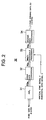
- Fig. 2 shows the internal configuration of the data conversion circuit 30.
- the data conversion circuit 30 includes an ABL (automatic brightness control) circuit 31, first data conversion circuit 32, multi-grayscale processing circuit 33, and second data conversion circuit 34.
- ABL automatic brightness control
- the ABL circuit 31 adjusts the brightness level of the pixel data PD for each pixel supplied in sequence from the A/D converter 4, such that the average brightness of the image displayed on the screen of the PDP 10 is within an appropriate brightness range, and supplies the brightness-adjusted pixel data PD BL obtained in this way to the first data conversion circuit 32.
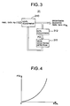
- Fig. 3 shows the internal configuration of the ABL circuit 31.
- the level adjustment circuit 310 outputs brightness-adjusted pixel data PD BL obtained by adjusting the level of the pixel data PD in accordance with the mean brightness determined by the mean brightness detection circuit 311 (will be described).
- the mean brightness detection circuit 311 determines the mean brightness of this inverse-gamma converted pixel data PDr, and supplies the level adjustment circuit 310 with mean brightness information indicating this mean brightness.
- the level adjustment circuit 310 supplies pixel data PD with the level adjusted according to this mean brightness information to the data conversion circuit 312 and to the first data conversion circuit 32 of the next stage, as the brightness-adjusted pixel data PD BL .
- the first data conversion circuit 32 converts the brightness-adjusted pixel data PD BL to 9 bits, from “0" to "384" of first conversion pixel data PD H , based on conversion characteristics as shown in Fig. 5, and supplies the resultant to the multi-grayscale processing circuit 33.
- the first data conversion circuit 32 performs data conversion according to the number of display grayscales in the multi-grayscale processing circuit 33 (will be described) and the number of compression bits in multi-grayscale processing. That is, brightness saturation due to the multi-grayscale processing of the multi-grayscale processing circuit 33, and the occurrence of flat portions in the display characteristic arising when display grayscales are not at bit boundaries (that is, the occurrence of grayscale distortion), are prevented.
- the multi-grayscale processing circuit 33 subjects the above 9 bits of first converted pixel data PD H to error-diffusion processing and dither processing (will be described), and by this means generates multi-grayscale-processed pixel data PD s with the number of grayscales maintained, but with the number of bits reduced to 4. This error-diffusion processing and dither processing are described below.
- the second data conversion circuit 34 converts the above 4 bits of multi-grayscale-processed pixel data PD s into pixel driving data GD including first through 12th bits, according to a conversion table as shown in Fig. 6. Each of these first through 12th bits corresponds to subfields SF1 to SF12 (will be described).
- pixel data PD which can represent 256 grayscales using 8 bits is converted into 12-bit pixel driving data GD including, in all, 13 patterns, as shown in Fig. 6.
- the memory 5 sequentially writes and stores the pixel driving data GD according to write signals supplied from the driving control circuit 2.
- the memory 5 sequentially reads and supplies to the address driver 6 one row's worth (one display line worth) of bits in the same digit (bit place) of the pixel driving data GD 11 to GD nm , in response to a read signal supplied from the driving control circuit 2.
- the memory 5 divides one screen's worth of pixel driving data GD 11 to GD nm , each comprising 12 bits, to be handled as pixel driving data bits DB1 11-nm to DB12 11-nm , as follows:
- bits DB1 11-nm , DB2 11-nm , ..., DB12 11-nm are then read sequentially one row at a time and supplied to the address driver 6, in response to read signals supplied by the driving control circuit 2.
- the driving control circuit 2 generates a clock signal for the A/D converter 4 and write and read signals for the memory 5, synchronized with the horizontal sync signal H and vertical sync signal V.
- the driving control circuit 2 supplies various timing signals to drive the PDP 10 to the address driver 6, first sustain driver 7, and second sustain driver 8, in accordance with the emission driving format shown in Fig. 7.
- the emission driving format shown in Fig. 7 divides one field in an image signal into 12 subfields, namely SF1 to SF12, and performs driving of the PDP 10 by subfields.
- each subfield comprises an address sequence Wc which sets each discharge cell of the PDP 10 to the "lit discharge cell state" or to the "extinguished discharge cell state", based on the input image signal, and an emission sustain sequence Ic which causes only those discharge cells in the "lit discharge cell state" to emit light for a period (number of times) corresponding to the weighting of the subfield.
- a simultaneous reset sequence Rc which initializes to the "lit discharge cell state" all discharge cells of the PDP 10 is executed only in the leading subfield SF1, and an extinction sequence E is executed only for the final subfield SF12.
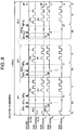
- Fig. 8 illustrates the timing for application of various driving pulses applied to the row electrodes and column electrodes of the PDP 10 by the address driver 6, first sustain driver 7, and second sustain driver 8, according to the emission driving format shown in Fig. 7.
- the first sustain driver 7 applies negative-polarity reset pulses RP x to the row electrodes X 1 to X n , as shown in Fig. 8.
- the second sustain driver 8 applies positive-polarity reset pulses RP Y to the row electrodes Y 1 to Y 2 , as shown in Fig. 8.
- All the discharge cells of the PDP 10 undergo reset discharge in response to application of these reset pulses RP X and RP Y , and a prescribed quantity of wall charge is formed uniformly within each of the discharge cells. By this means, all the discharge cells are initialized to the "lit discharge cell state".
- the address driver 6 generates pixel data pulses having a voltage corresponding to the logical level of the pixel driving data bits DB supplied from the memory 5. For example, when the logical level of the pixel driving data bit DB is "1", the address driver 6 generates a high-voltage pixel data pulse, and when it is "0" generates a low-voltage (0 V) pixel data pulse.
- the address driver 6 applies a pixel data pulse group DP, comprising one row's (one display line's) worth of pixel data pulses, to the column electrodes D 1 to D m .
- a pixel data pulse group DP1 1 comprising m pixel data pulses corresponding to the logical levels of these bits DB1 11-1m , is applied to the column electrodes D 1-m .
- bits DB1 21-2m which are the portion corresponding to the second row (display line) of the pixel driving data bits DB1 11-nm are extracted, and a pixel data pulse group DP1 2 comprising m pixel data pulses corresponding to the logical levels of these bits DB1 21-2m is applied to the column electrodes D 1-m .
- pixel data pulse groups DP1 3 to DP1 n for each row (display line) are applied in sequence to the column electrodes D 1 to D m in the address sequence Wc for the subfield SF1.
- the second sustain driver 8 In the address sequence Wc the second sustain driver 8 generates negative-polarity scan pulses SP as shown in Fig. 8, with the same timing as the timing for application of the above-described pixel data pulse groups DP, and applies the scan pulses SP sequentially to the row electrodes Y 1 to Y n .
- discharge selected elimination discharge
- discharge occurs only in those discharge cells at intersections between the row electrodes to which scan pulses SP are applied, and column electrodes to which high-voltage pixel data pulses are applied, and the wall charge remaining in these discharge cells is (selectively) eliminated (removed, erased).
- each of the 1st through 12th bits in the pixel driving data GD determines whether selected elimination discharge is to be induced in the address sequence Wc in each of the subfields SF1 to SF12. Discharge cells which have been initialized to the "lit discharge cell state" in the simultaneous reset sequence Rc make a transition to the "extinguished discharge cell state" as a result of this selected elimination discharge. On the other hand, discharge cells in which the selected elimination discharge has not been induced are maintained in the state initialized in the simultaneous reset sequence Rc, that is, in the "lit discharge cell state".
- the first sustain driver 7 and the second sustain driver 8 alternately apply positive-polarity sustain pulses IP X and IP Y to the row electrodes X 1 to X n and Y 1 to Y n , as shown in Fig. 8.
- the number of sustain pulses IP applied in the emission sustain sequence Ic is, for the respective subfields SF1 to SF12, as follows.
- the elimination sequence E is executed only for the final subfield SF12.
- the address driver 6 generates and applies positive-polarity elimination pulses AP to the column electrodes D 1 to D m , as shown in Fig. 8.
- the second sustain driver 8 generates negative-polarity elimination pulses EP simultaneously with the timing of application of these elimination pulses AP, as shown in Fig. 8, and applies the elimination pulses EP to the row electrodes Y 1 to Y n .
- elimination discharge is induced in all the discharge cells in the PDP 10, and the wall charge remaining in all the discharge cells is annihilated.
- all the discharge cells in the PDP 10 enter the "extinguished discharge cell state".
- each discharge cell is set in the "lit discharge cell state” or in the "extinguished discharge cell state” is determined by the pixel driving data GD, as shown in Fig. 6. That is, when a bit in the pixel driving data GD is at logical level "1", selected elimination discharge is induced in the address sequence Wc of the subfield corresponding to the digit position for that bit (bit place), and the discharge cell is set in the "extinguished discharge cell state". On the other hand, when the logical level for the bit is "0", the selected elimination discharge is not induced, and the current state is maintained.
- each discharge cell is in the "lit discharge cell state" in a period from the beginning of the first field until the inducement of selected elimination discharge in the subfield indicated by the black circle in Fig. 6.
- emission sustain sequence Ic existing during this period for each subfield, indicated by a white circle, emission occurs the number of times described above.
- the brightness of the grayscale is represented by the total number of emissions executed in each of the subfields SF1 to SF12 within one field.
- the intermediate brightnesses of 13 grayscales can be represented, as follows: 0:1:3:7:14:25:39:59:84:117:157:205:255
- the pixel data obtained based on the image signal is 8 bits; 256 halftones can be made.
- Multi-grayscale processing is performed by the multi-grayscale processing circuit 33 in order to allow the driving scheme utilized in representing (expressing) the above-mentioned 13 intermediate brightnesses to also represent approximately 256 grayscales' worth of halftones in a pseudo fashion.
- Fig. 9 shows the internal configuration of this multi-grayscale processing circuit 33.
- the multi-grayscale processing circuit 33 includes an RGB data separation circuit 331, error diffusion processing circuit 332, RGB data multiplexing circuit 333, and dither processing circuit 340.
- the RGB data separation circuit 331 separates and extracts data for red emission, data for green emission, and data for blue emission from the series of first converted pixel data PD H supplied by the first data conversion circuit 32.
- the RGB data separation circuit 331 supplies data for red emission to the error diffusion processing circuit 332R as red pixel data PD HR .
- the RGB data separation circuit 331 supplies data for green emission to the error diffusion processing circuit 332G as green pixel data PD HG , and supplies data for blue emission to the error diffusion processing circuit 332B as blue pixel data PD HB .
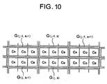
- the error diffusion processing circuit 332R first extracts red pixel data corresponding to red discharge cells C R at each of the pixels G(j,k), G(j,k-1), G(j-1,k-1), G(j-1,k), and G(j-1,k+1) in the PDP 10, as shown in Fig. 10, from the series of red pixel data PD HR supplied by the RGB data separation circuit 331. Next, taking as the lowest bit the digit-carry bit (of single bit worth) obtained when weighting and adding the respective lower two bits of the red pixel data corresponding to these pixels, this lowest bit is added to the upper 7 bits of the red pixel data corresponding to the red discharge cell C R of the pixel G(j,k), to obtain 8-bit data.
- the error diffusion processing circuit 332R supplies these 8 data bits to the dither processing circuit 340 as error diffusion-processed pixel data ED R .
- the error diffusion processing circuit 332G first extracts green pixel data corresponding to green discharge cells C G at each of the pixels G(j,k), G(j,k-1), G(j-1,k-1), G(j-1,k), and G(j-1,k+1) in the PDP 10, as shown in Fig. 10, from the series of green pixel data PD HG supplied by the RGB data separation circuit 331.
- the lowest bit is are added to the upper 7 bits of the green pixel data corresponding to the green discharge cell C G of the pixel G(j,k), to obtain 8-bit data.
- the error diffusion processing circuit 332G supplies these 8 data bits to the dither processing circuit 340 as error diffusion-processed pixel data ED G .
- the error diffusion processing circuit 332B first extracts blue pixel data corresponding to blue discharge cells C B at each of the pixels G(j,k), G(j,k-1), G(j-1,k-1), G(j-1,k), and G(j-1,k+1) in the PDP 10, as shown in Fig. 10, from the series of blue pixel data PD HB supplied by the RGB data separation circuit 331. Next, taking as the lowest bit the digit-carry bit obtained when weighting and adding the respective lower two bits of the blue pixel data corresponding to these pixels, the lowest bit is added to the upper 7 bits of the blue pixel data corresponding to the blue discharge cell C B of the pixel G(j,k), to obtain 8-bit data. The error diffusion processing circuit 332B supplies the 8-bit data to the dither processing circuit 340 as error diffusion-processed pixel data ED B .
- the error diffusion processing circuit 332 reflects, in the pixel data corresponding to the pixel G(j,k), the result of weighting and adding the lowest data bits of the pixels G(j,k-1), G(j-1,k+1), G(j-1,k), and G(j-1,k-1) surrounding the pixel G(j,k).
- the brightness component corresponding to the lowest two bits for the pixel G(j,k) are approximately (in a pseudo manner) represented by the peripheral pixels.
- the dither processing circuit 340 includes dither matrix circuits (341R, 341G and 341B), adders (342R, 342G and 342B), and upper bit extraction circuits (343R, 343G and 343B).
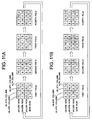
- the dither matrix circuits 341R and 341B generate 4-bit dither coefficients able to represent, for each 4-row by 4-column pixel group of the PDP 10, "0" to "15” corresponding to sixteen pixel positions within the pixel group, as shown in Fig. 11A. That is, as shown in Fig. 11A, the dither matrix circuits 341R and 341B generate dither coefficients "15", "7", "13", "5" for pixels belonging to the (4L-3)th column, (4L-2)th column, (4L-1)th column, and the 4Lth column in the (4K-3)th row of the PDP 10, in the first field.
- the dither matrix circuits 341R and 341B generate dither coefficients "1", “9”, “3”, "11” for pixels belonging to the (4L-3)th column, (4L-2)th column, (4L-1)th column, and the 4Lth column in the (4K-2)th row of the PDP 10.
- the dither matrix circuits 341R and 341B generate dither coefficients "13", "5", "15”, "7” corresponding to pixels belonging to the (4L-3)th column, (4L-2)th column, (4L-1)th column, and the 4Lth column in the (4K-1)th row of the PDP 10.
- the dither matrix circuits 341R and 341B generate dither coefficients "3", "11”, “1”, “9” corresponding to pixels belonging to the (4L-3)th column, (4L-2)th column, (4L-1)th column, and the 4Lth column in the 4Kth row of the PDP 10.
- K represents a natural number from 1 to n/4
- L represents a natural number from 1 to m/4.
- the dither matrix circuits 341R and 341B generate dither coefficients "10", "2", “8”, "0” corresponding to pixels belonging to the (4L-3)th column, (4L-2)th column, (4L-1)th column, and the 4Lth column in the (4K-3)th row of the PDP 10.
- the dither matrix circuits 341R and 341B generate dither coefficients "2", "12", “6”, "14” corresponding to pixels belonging to the (4L-3)th column, (4L-2)th column, (4L-1)th column, and the 4Lth column in the (4K-2)th row of the PDP 10.
- the dither matrix circuits 341R and 341B generate dither coefficients "8", "0”, "10", "2" corresponding to pixels belonging to the (4L-3)th column, (4L-2)th column, (4L-1)th column, and the 4Lth column in the (4K-1)th row of the PDP 10.
- the dither matrix circuits 341R and 341B generate dither coefficients "6", "14", "4", "12” corresponding to pixels belonging to the (4L-3)th column, (4L-2)th column, (4L-1)th column, and the 4Lth column in the 4Kth row of the PDP 10.
- the dither matrix circuits 341R and 341B generate dither coefficients "13", "5", "15”, "7” corresponding to pixels belonging to the (4L-3)th column, (4L-2)th column, (4L-1)th column, and the 4Lth column in the (4K-3)th row of the PDP 10.
- the dither matrix circuits 341R and 341B generate dither coefficients "3", "11”, “1”, “9” corresponding to pixels belonging to the (4L-3)th column, (4L-2)th column, (4L-1)th column, and the 4Lth column in the (4K-2)th row of the PDP 10.
- the dither matrix circuits 341R and 341B generate dither coefficients "15”, "7”, “13”, "5" corresponding to pixels belonging to the (4L-3)th column, (4L-2)th column, (4L-1)th column, and the 4Lth column in the (4K-1)th row of the PDP 10.
- the dither matrix circuits 341R and 341B generate dither coefficients "1", “9”, “3”, “11” corresponding to pixels belonging to the (4L-3)th column, (4L-2)th column, (4L-1)th column, and the 4Lth column in the 4Kth row of the PDP 10.
- the dither matrix circuits 341R and 341B generate dither coefficients "8", "0”, “10”, "2" corresponding to pixels belonging to the (4L-3)th column, (4L-2)th column, (4L-1)th column, and the 4Lth column in the (4K-3)th row of the PDP 10.
- the dither matrix circuits 341R and 341B generate dither coefficients "6", "14", "4", "12” corresponding to pixels belonging to the (4L-3)th column, (4L-2)th column, (4L-1)th column, and the 4Lth column in the (4K-2)th row of the PDP 10.
- the dither matrix circuits 341R and 341B generate dither coefficients "10", "2", “8”, "0” corresponding to pixels belonging to the (4L-3)th column, (4L-2)th column, (4L-1)th column, and the 4Lth column in the (4K-1)th row of the PDP 10.
- the dither matrix circuits 341R and 341B generate dither coefficients "4", "12”, “6”, "14” corresponding to pixels belonging to the (4L-3)th column, (4L-2)th column, (4L-1)th column, and the 4Lth column in the 4Kth row of the PDP 10.
- the dither matrix circuits 341R and 341B repeatedly execute a series of operations to generate dither coefficients in the first through fourth fields, as shown in Fig. 11A.
- the dither matrix circuit 341R supplies the generated dither coefficients to the adder 342R with timing matched to the error diffusion-processed pixel data ED R supplied corresponding to the red discharge cells within each pixel in a 4-row by 4-column pixel group.
- the adder 342R adds the error diffusion-processed pixel data ED R and the dither coefficients shown in Fig. 11A generated by the dither matrix circuit 341R, and supplies the resulting dither-added red pixel data DD R to the upper bit extraction circuit 343R.
- the upper bit extraction circuit 343R extracts the upper 4 bits from the dither-added red pixel data DD R , and supplies this upper 4 bits to the RGB data multiplexing circuit 333 as multi-grayscale red pixel data PD SR .
- the dither matrix circuit 341B supplies the generated dither coefficients to the adder 342B with timing matched to the error diffusion-processed pixel data ED B supplied corresponding to the blue discharge cells within each pixel in a 4-row by 4-column pixel group.
- the adder 342B adds the error diffusion-processed pixel data ED B and the dither coefficients shown in Fig. 11A generated by the dither matrix circuit 341B, and supplies the resulting dither-added blue pixel data DD B to the upper bit extraction circuit 343B.
- the upper bit extraction circuit 343B extracts the upper 4 bits from the dither-added blue pixel data DD B , and supplies this upper 4 bits to the RGB data multiplexing circuit 333 as multi-grayscale blue pixel data PD SB .
- the dither matrix circuit 341G generates dither coefficients as shown in Fig. 11B, which are different from those of the dither matrix circuits 341R and 341B. That is, as shown in Fig. 11B, in the first field the dither matrix circuit 341G generates dither coefficients "2", "8", "0", "10" for pixels belonging to the (4L-3)th column, (4L-2)th column, (4L-1)th column, and the 4Lth column in the (4K-3)th row of the PDP 10.
- the dither matrix circuit 341G In this first field the dither matrix circuit 341G generates dither coefficients "12", “6", “14”, "4" for pixels belonging to the (4L-3)th column, (4L-2)th column, (4L-1)th column, and the 4Lth column in the (4K-2)th row of the PDP 10.
- the dither matrix circuit 341G In this first field the dither matrix circuit 341G generates dither coefficients "0", "10", “2”, “8” for pixels belonging to the (4L-3)th column, (4L-2)th column, (4L-1)th column, and the 4Lth column in the (4K-1)th row of the PDP 10.
- the dither matrix circuit 341G In this first field the dither matrix circuit 341G generates dither coefficients "14", "4", "12”, “6” corresponding to pixels belonging to the (4L-3)th column, (4L-2)th column, (4L-1)th column, and the 4Lth column in the 4Kth row of the PDP 10.
- the dither matrix circuit 341G In the second field the dither matrix circuit 341G generates dither coefficients "5", "15”, “7”, “13” corresponding to pixels belonging to the (4L-3)th column, (4L-2)th column, (4L-1)th column, and the 4Lth column in the (4K-3)th row of the PDP 10.
- the dither matrix circuit 341G In this second field the dither matrix circuit 341G generates dither coefficients "11", “1", “9”, "3" corresponding to pixels belonging to the (4L-3)th column, (4L-2)th column, (4L-1)th column, and the 4Lth column in the (4K-2)th row of the PDP 10.
- the dither matrix circuit 341G In this second field the dither matrix circuit 341G generates dither coefficients "7", "13", "5", "15” corresponding to pixels belonging to the (4L-3)th column, (4L-2)th column, (4L-1)th column, and the 4Lth column in the (4K-1)th row of the PDP 10.
- the dither matrix circuit 341G In this second field the dither matrix circuit 341G generates dither coefficients "9", "3", “11”, "1” corresponding to pixels belonging to the (4L-3)th column, (4L-2)th column, (4L-1)th column, and the 4Lth column in the 4Kth row of the PDP 10.
- the dither matrix circuit 341G In the third field the dither matrix circuit 341G generates dither coefficients "0", "10", “2”, “8” corresponding to pixels belonging to the (4L-3)th column, (4L-2)th column, (4L-1)th column, and the 4Lth column in the (4K-3)th row of the PDP 10.
- the dither matrix circuit 341G generates dither coefficients "14", "4", "12”, “6” corresponding to pixels belonging to the (4L-3)th column, (4L-2)th column, (4L-1)th column, and the 4Lth column in the (4K-2)th row of the PDP 10.
- the dither matrix circuit 341G generates dither coefficients "2", "8”, “0”, "0” corresponding to pixels belonging to the (4L-3)th column, (4L-2)th column, (4L-1)th column, and the 4Lth column in the (4K-1)th row of the PDP 10.
- the dither matrix circuit 341G generates dither coefficients "12", “6”, “14”, "4" corresponding to pixels belonging to the (4L-3)th column, (4L-2)th column, (4L-1)th column, and the 4Lth column in the 4Kth row of the PDP 10.
- the dither matrix circuit 341G In the fourth field the dither matrix circuit 341G generates dither coefficients "7", "13", "5", "15” corresponding to pixels belonging to the (4L-3)th column, (4L-2)th column, (4L-1)th column, and the 4Lth column in the (4K-3)th row of the PDP 10.
- the dither matrix circuit 341G generates dither coefficients "9", "3", “11”, "1” corresponding to pixels belonging to the (4L-3)th column, (4L-2)th column, (4L-1)th column, and the 4Lth column in the (4K-2)th row of the PDP 10.
- the dither matrix circuit 341G In this fourth field the dither matrix circuit 341G generates dither coefficients "5", "15”, “7”, “13” corresponding to pixels belonging to the (4L-3)th column, (4L-2)th column, (4L-1)th column, and the 4Lth column in the (4K-1)th row of the PDP 10.
- the dither matrix circuit 341G generates dither coefficients "11", “1”, “9”, “3" corresponding to pixels belonging to the (4L-3)th column, (4L-2)th column, (4L-1)th column, and the 4Lth column in the 4Kth row of the PDP 10.
- the dither matrix circuit 341G repeatedly execute a series of operations to generate dither coefficients in the first through fourth fields, as shown in Fig. 11B. Also, the dither matrix circuit 341G supplies the generated dither coefficients to the adder 342G with timing matched to the error diffusion-processed pixel data ED G supplied corresponding to the green discharge cells within each pixel in a 4-row by 4-column pixel group.
- the adder 342G adds the error diffusion-processed pixel data ED G and the dither coefficients shown in Fig. 11B generated by the dither matrix circuit 341G, and supplies the resulting dither-added green pixel data DD G to the upper bit extraction circuit 343G.
- the upper bit extraction circuit 343G extracts the upper 4 bits from the dither-added green pixel data DD G , and supplies this upper 4 bits to the RGB data multiplexing circuit 333 as multi-grayscale green pixel data PD SG .
- the RGB data multiplexing circuit 333 performs time-division multiplexing of the multi-grayscale red pixel data PD SR , multi-grayscale green pixel data PD SG , and multi-grayscale blue pixel data PD SB , in order, and outputs the resulting data train to the second data conversion circuit 34 as the multi-grayscale processed pixel data PD s , as shown in Fig. 2.
- the dither processing circuit 340 adds 4-bit dither coefficients from "0" to "15", as shown in Fig. 11A, to the lower 4 bits of the error diffusion-processed pixel data ED R and ED B .
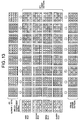
- digit carrying which occurs when the 4-bit dither coefficients are added to the lower 4 bits of the error diffusion-processed pixel data ED R (or ED B ) takes a form like that shown in Fig. 12. It should be noted in Fig.
- the first case shows where the lower 4 bits are all "0" for all of the 16 error diffusion-processed pixel data ED corresponding to 16 pixels in a 4-row by 4-column pixel group
- the second case shows where the lower 4 bits are all "1”
- the third case shows where the lower 4 bits are all "2”
- the fourth case shows where the lower 4 bits are all "3”
- the fifth case shows where the lower 4 bits are all "4"
- the sixth case shows where the lower 4 bits are all "5"
- the seventh case shows where the lower 4 bits are all "6”
- the eighth case shows where the lower 4 bits are all "7”.
- Carrying is reflected in the upper 4 bits of both the dither-added red pixel data DD R and the dither-added blue pixel data DD B .
- intermediate brightnesses equivalent to 7 bits can be represented (expressed), based on the 4-bit multi-grayscale red pixel data PD SR and multi-grayscale blue pixel data PD SB .
- the patterns of dither coefficients added within 4-row by 4-column pixel groups differ for each of the first to fourth fields, so that the digit carry pattern makes a transition from the first field to the fourth field, as shown in Fig. 12.
- a dither pattern is visually represented on the screen of the PDP 10, as shown in Fig. 12.
- intermediate brightnesses equivalent to 7 bits can be represented based on the 4-bit multi-grayscale green pixel data PD G .
- the pattern of the dither coefficients added in a 4-row by 4-column pixel group is different for each of the first to the fourth fields, so that the bit-carry pattern also changes from the first to the fourth fields, as shown in Fig. 13.
- a dither pattern like that shown in Fig. 13 is visually represented on the screen of the PDP 10.
- the dither pattern which appears visually on the screen is different from that shown in Fig. 12. That is, as shown in Fig.
- the dither pattern perceived as a result of emission by green discharge cells C G formed in each pixel is different from the dither pattern perceived as a result of emission by red discharge cells C R and blue discharge cells C B (Fig. 12). Consequently different dither patterns are intermixed within a single screen, as shown in Fig. 12 and Fig. 13, and no specific dither pattern is perceived.
Landscapes
- Engineering & Computer Science (AREA)
- Physics & Mathematics (AREA)
- Computer Hardware Design (AREA)
- General Physics & Mathematics (AREA)
- Theoretical Computer Science (AREA)
- Power Engineering (AREA)
- Plasma & Fusion (AREA)
- Control Of Indicators Other Than Cathode Ray Tubes (AREA)
- Control Of Gas Discharge Display Tubes (AREA)
- Transforming Electric Information Into Light Information (AREA)
- Control Of El Displays (AREA)
Applications Claiming Priority (2)
| Application Number | Priority Date | Filing Date | Title |
|---|---|---|---|
| JP2001161994A JP2002351381A (ja) | 2001-05-30 | 2001-05-30 | ディスプレイ装置及びディスプレイパネルの駆動方法 |
| JP2001161994 | 2001-05-30 |
Publications (2)
| Publication Number | Publication Date |
|---|---|
| EP1262943A2 true EP1262943A2 (fr) | 2002-12-04 |
| EP1262943A3 EP1262943A3 (fr) | 2004-08-11 |
Family
ID=19005189
Family Applications (1)
| Application Number | Title | Priority Date | Filing Date |
|---|---|---|---|
| EP02010751A Withdrawn EP1262943A3 (fr) | 2001-05-30 | 2002-05-14 | Panneau d'affichage à plasma et son procédé de commande |
Country Status (3)
| Country | Link |
|---|---|
| US (1) | US20020180754A1 (fr) |
| EP (1) | EP1262943A3 (fr) |
| JP (1) | JP2002351381A (fr) |
Cited By (2)
| Publication number | Priority date | Publication date | Assignee | Title |
|---|---|---|---|---|
| EP1521450A2 (fr) | 2003-09-30 | 2005-04-06 | Sharp Kabushiki Kaisha | Système et procédés pour la création d'une structure de tramage multi-dimensionnelle et application |
| EP1542199A3 (fr) * | 2003-12-08 | 2008-10-08 | LG Electronics Inc. | Méthode et dispositif de commande d'un panneau d'affichage à plasma |
Families Citing this family (11)
| Publication number | Priority date | Publication date | Assignee | Title |
|---|---|---|---|---|
| US7443365B2 (en) | 2003-01-06 | 2008-10-28 | Matsushita Electric Industrial Co., Ltd. | Display unit and display method |
| JP4606735B2 (ja) * | 2003-01-06 | 2011-01-05 | パナソニック株式会社 | 表示装置および表示方法 |
| EP1439517A1 (fr) * | 2003-01-10 | 2004-07-21 | Deutsche Thomson-Brandt Gmbh | Appareil et procédé de traitement de données vidéo destinées à être visualisées sur écran |
| KR100490625B1 (ko) * | 2003-02-20 | 2005-05-17 | 삼성에스디아이 주식회사 | 화상 표시 장치 |
| KR100499102B1 (ko) * | 2003-12-15 | 2005-07-01 | 엘지전자 주식회사 | 플라즈마 디스플레이 패널의 구동장치 및 구동방법 |
| JP2006039039A (ja) * | 2004-07-23 | 2006-02-09 | Tohoku Pioneer Corp | 自発光表示パネルの駆動装置、駆動方法及びその駆動装置を備えた電子機器 |
| JP2006065093A (ja) * | 2004-08-27 | 2006-03-09 | Tohoku Pioneer Corp | 自発光表示パネルの駆動装置、駆動方法及びその駆動装置を備えた電子機器 |
| KR100612388B1 (ko) * | 2004-08-30 | 2006-08-16 | 삼성에스디아이 주식회사 | 표시 장치 및 그 구동 방법 |
| JP4753353B2 (ja) * | 2005-03-31 | 2011-08-24 | 東北パイオニア株式会社 | 自発光表示パネルの駆動装置、駆動方法及びその駆動装置を備えた電子機器 |
| KR100794161B1 (ko) | 2006-01-06 | 2008-01-11 | 엘지전자 주식회사 | 플라즈마 디스플레이 장치 및 그 화상처리 방법 |
| CN110473493B (zh) * | 2019-08-30 | 2021-04-06 | 上海中航光电子有限公司 | 显示面板的驱动方法及显示装置 |
Family Cites Families (7)
| Publication number | Priority date | Publication date | Assignee | Title |
|---|---|---|---|---|
| JP3618024B2 (ja) * | 1996-09-20 | 2005-02-09 | パイオニア株式会社 | 自発光表示器の駆動装置 |
| JPH1098662A (ja) * | 1996-09-20 | 1998-04-14 | Pioneer Electron Corp | 自発光表示器の駆動装置 |
| US6034664A (en) * | 1997-06-25 | 2000-03-07 | Sun Microsystems, Inc. | Method and apparatus for pseudo-random noise generation based on variation of intensity and coloration |
| JP3750889B2 (ja) * | 1997-07-02 | 2006-03-01 | パイオニア株式会社 | ディスプレイパネルの中間調表示方法 |
| US6219838B1 (en) * | 1998-08-24 | 2001-04-17 | Sharewave, Inc. | Dithering logic for the display of video information |
| JP3606429B2 (ja) * | 1999-02-19 | 2005-01-05 | パイオニア株式会社 | プラズマディスプレイパネルの駆動方法 |
| US6894698B2 (en) * | 2000-01-11 | 2005-05-17 | Sun Microsystems, Inc. | Recovering added precision from L-bit samples by dithering the samples prior to an averaging computation |
-
2001
- 2001-05-30 JP JP2001161994A patent/JP2002351381A/ja active Pending
-
2002
- 2002-05-14 EP EP02010751A patent/EP1262943A3/fr not_active Withdrawn
- 2002-05-24 US US10/153,789 patent/US20020180754A1/en not_active Abandoned
Cited By (2)
| Publication number | Priority date | Publication date | Assignee | Title |
|---|---|---|---|---|
| EP1521450A2 (fr) | 2003-09-30 | 2005-04-06 | Sharp Kabushiki Kaisha | Système et procédés pour la création d'une structure de tramage multi-dimensionnelle et application |
| EP1542199A3 (fr) * | 2003-12-08 | 2008-10-08 | LG Electronics Inc. | Méthode et dispositif de commande d'un panneau d'affichage à plasma |
Also Published As
| Publication number | Publication date |
|---|---|
| EP1262943A3 (fr) | 2004-08-11 |
| JP2002351381A (ja) | 2002-12-06 |
| US20020180754A1 (en) | 2002-12-05 |
Similar Documents
| Publication | Publication Date | Title |
|---|---|---|
| US6906726B2 (en) | Display device | |
| US6646625B1 (en) | Method for driving a plasma display panel | |
| EP0952569A2 (fr) | Méthode de commande d'un panneau d'affichage à plasma | |
| JPH1173157A (ja) | ディスプレイパネルの中間調表示方法 | |
| US6593903B2 (en) | Method for driving a plasma display panel | |
| EP0831449A2 (fr) | Appareil de commande pour un dispositif d'affichage luminescent | |
| US6642911B2 (en) | Plasma display panel driving method | |
| US7006058B2 (en) | Method of driving a plasma display panel | |
| US7333076B2 (en) | Method for driving display panel | |
| JP3961171B2 (ja) | ディスプレイ装置の多階調処理回路 | |
| US20020180754A1 (en) | Display device and display panel driving method | |
| JP2000267627A (ja) | プラズマディスプレイパネルの駆動方法 | |
| JP2000231362A (ja) | プラズマディスプレイパネルの駆動方法 | |
| JP3678401B2 (ja) | プラズマディスプレイパネルの駆動方法 | |
| JP2005321442A (ja) | ディスプレイ装置のディザ処理回路 | |
| JP3578323B2 (ja) | プラズマディスプレイパネルの駆動方法 | |
| US6982732B2 (en) | Display panel driving method with selectable driving pattern | |
| JP3734244B2 (ja) | ディスプレイパネルの駆動方法 | |
| US7142174B2 (en) | Driving method of plasma display panel | |
| JP2003076319A (ja) | プラズマディスプレイパネルの駆動方法 | |
| JP4731841B2 (ja) | 表示パネルの駆動装置及び駆動方法 | |
| JP4731738B2 (ja) | 表示装置 | |
| US7576714B2 (en) | Display-panel driving method | |
| JP3672292B2 (ja) | プラズマディスプレイパネルの駆動方法 | |
| JP3868457B2 (ja) | ディスプレイパネルの駆動方法 |
Legal Events
| Date | Code | Title | Description |
|---|---|---|---|
| PUAI | Public reference made under article 153(3) epc to a published international application that has entered the european phase |
Free format text: ORIGINAL CODE: 0009012 |
|
| AK | Designated contracting states |
Kind code of ref document: A2 Designated state(s): AT BE CH CY DE DK ES FI FR GB GR IE IT LI LU MC NL PT SE TR |
|
| AX | Request for extension of the european patent |
Free format text: AL;LT;LV;MK;RO;SI |
|
| RAP1 | Party data changed (applicant data changed or rights of an application transferred) |
Owner name: PIONEER DISPLAY PRODUCTS CORPORATION Owner name: PIONEER CORPORATION |
|
| PUAL | Search report despatched |
Free format text: ORIGINAL CODE: 0009013 |
|
| AK | Designated contracting states |
Kind code of ref document: A3 Designated state(s): AT BE CH CY DE DK ES FI FR GB GR IE IT LI LU MC NL PT SE TR |
|
| AX | Request for extension of the european patent |
Extension state: AL LT LV MK RO SI |
|
| AKX | Designation fees paid | ||
| REG | Reference to a national code |
Ref country code: DE Ref legal event code: 8566 |
|
| STAA | Information on the status of an ep patent application or granted ep patent |
Free format text: STATUS: THE APPLICATION IS DEEMED TO BE WITHDRAWN |
|
| 18D | Application deemed to be withdrawn |
Effective date: 20050212 |