EP0833343A2 - An einem Subdekodierer eines Halbleiterspeichers angekoppeltes NOR-Gatter - Google Patents
An einem Subdekodierer eines Halbleiterspeichers angekoppeltes NOR-Gatter Download PDFInfo
- Publication number
- EP0833343A2 EP0833343A2 EP97116881A EP97116881A EP0833343A2 EP 0833343 A2 EP0833343 A2 EP 0833343A2 EP 97116881 A EP97116881 A EP 97116881A EP 97116881 A EP97116881 A EP 97116881A EP 0833343 A2 EP0833343 A2 EP 0833343A2
- Authority
- EP
- European Patent Office
- Prior art keywords
- gate
- decoder
- power supply
- mos transistor
- node
- Prior art date
- Legal status (The legal status is an assumption and is not a legal conclusion. Google has not performed a legal analysis and makes no representation as to the accuracy of the status listed.)
- Withdrawn
Links
Images




Classifications
-
- G—PHYSICS
- G11—INFORMATION STORAGE
- G11C—STATIC STORES
- G11C11/00—Digital stores characterised by the use of particular electric or magnetic storage elements; Storage elements therefor
- G11C11/21—Digital stores characterised by the use of particular electric or magnetic storage elements; Storage elements therefor using electric elements
- G11C11/34—Digital stores characterised by the use of particular electric or magnetic storage elements; Storage elements therefor using electric elements using semiconductor devices
- G11C11/40—Digital stores characterised by the use of particular electric or magnetic storage elements; Storage elements therefor using electric elements using semiconductor devices using transistors
- G11C11/41—Digital stores characterised by the use of particular electric or magnetic storage elements; Storage elements therefor using electric elements using semiconductor devices using transistors forming static cells with positive feedback, i.e. cells not needing refreshing or charge regeneration, e.g. bistable multivibrator or Schmitt trigger
- G11C11/413—Auxiliary circuits, e.g. for addressing, decoding, driving, writing, sensing, timing or power reduction
- G11C11/417—Auxiliary circuits, e.g. for addressing, decoding, driving, writing, sensing, timing or power reduction for memory cells of the field-effect type
- G11C11/418—Address circuits
-
- G—PHYSICS
- G11—INFORMATION STORAGE
- G11C—STATIC STORES
- G11C11/00—Digital stores characterised by the use of particular electric or magnetic storage elements; Storage elements therefor
- G11C11/21—Digital stores characterised by the use of particular electric or magnetic storage elements; Storage elements therefor using electric elements
- G11C11/34—Digital stores characterised by the use of particular electric or magnetic storage elements; Storage elements therefor using electric elements using semiconductor devices
- G11C11/40—Digital stores characterised by the use of particular electric or magnetic storage elements; Storage elements therefor using electric elements using semiconductor devices using transistors
-
- G—PHYSICS
- G11—INFORMATION STORAGE
- G11C—STATIC STORES
- G11C8/00—Arrangements for selecting an address in a digital store
- G11C8/10—Decoders
-
- H—ELECTRICITY
- H03—ELECTRONIC CIRCUITRY
- H03K—PULSE TECHNIQUE
- H03K19/00—Logic circuits, i.e. having at least two inputs acting on one output; Inverting circuits
- H03K19/02—Logic circuits, i.e. having at least two inputs acting on one output; Inverting circuits using specified components
- H03K19/08—Logic circuits, i.e. having at least two inputs acting on one output; Inverting circuits using specified components using semiconductor devices
- H03K19/094—Logic circuits, i.e. having at least two inputs acting on one output; Inverting circuits using specified components using semiconductor devices using field-effect transistors
- H03K19/0944—Logic circuits, i.e. having at least two inputs acting on one output; Inverting circuits using specified components using semiconductor devices using field-effect transistors using MOSFET or insulated gate field-effect transistors, i.e. IGFET
- H03K19/0948—Logic circuits, i.e. having at least two inputs acting on one output; Inverting circuits using specified components using semiconductor devices using field-effect transistors using MOSFET or insulated gate field-effect transistors, i.e. IGFET using CMOS or complementary insulated gate field-effect transistors
Definitions
- the present invention relates to a NOR gate applied for a sub-decoder which drives word lines of a semiconductor memory cell array.
- FIG. 4 is a block diagram illustrating a typical configuration of a decoder circuit for driving word lines of a memory cell array.
- this decoder circuit consists of a hierarchical composition of a pre-decoder 401, a main decoder 402 and a sub-decoder 403 which is provided for each memory cell array 404 of a semiconductor memory.
- the pre-decoder 401 and the main decoder 402 composed of NOR gates and inverters, for example, decode the word line address signal for outputting four pre-decoder signals S10 to S13 corresponding to two bits A10 and A11 of the ten bits and 256 main decoder signals S0-0 to S0-255 corresponding to other eight bits A00 to A07 of the ten bits, respectively, to be supplied to the sub-decoder 403.
- One of the pre-decoder signals S10 to S13 and one of the main decoder signals S0-0 to S0-255 become at logic LOW when a word line is indicated by the ten bits A10, A11 and A01 to A07, and the corresponding memory cell array 404 is indicated by other bits of the word line address signal than the ten bits, so as to make the word line active. Therefore, load capacitance of a word line, which is made active only in a selected memory cell array, can be designed to be small with the decoder circuit of FIG. 4.
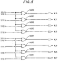
- FIG. 5 is a circuit diagram illustrating a part of the sub-decoder 403 where the four pre-decoder signals S10 to S13 and two (S0-0 and S0-1) of the main decoder signals are supplied.
- the sub-decoder 403 comprises eight NOR gates NOR0 to NOR7.
- Each of the NOR gates NOR0 to NOR3 makes active corresponding each of word lines WL0 to WL3 according to NOR logic of the main decoder signal S0-0 and each of the pre-decoder signals S10 to S13 supplied thereto, and each of the NOR gates NOR4 to NOR7 makes active corresponding each of word lines WL4 to WL7 according to NOR logic of the main decoder signal S0-1 and each of the pre-decoder signals S10 to S13, in the same way.
- both of the main decoder signals S0-0 and S0-1 are at logic HIGH, or every of the pre-decoder signals S10 to S13 is at logic HIGH.
- FIG. 6 is a timing chart illustrating a transition of logic of the main decoder signals S0-0 and S0-1 and the pre-decoder signals S10 to S13 when the selected word line changes from the word line WL0 to the word line WL1.
- the word line WL0 is made active at logic HIGH (Vcc), the main decoder signal S0-0 and the pre-decoder signal S10 being at logic LOW (Vss) and the other signals at logic HIGH.
- the pre-decoder signal S10 is turned to HIGH and another pre-decoder signal S11 is turned to LOW, the other signals remaining unchanged, for making active the word line WL1 instead of the word line WL0.
- every of the 2 10 word lines for example, is selected by making at logic LOW one of the pre-decoder signals S10 to S13 and one of the main decoder signals S0-0 to S0-255.
- logic HIGH corresponds to a high level power supply voltage Vcc
- logic LOW corresponding to a negative power supply voltage Vss.
- FIG. 7 is a circuit diagram illustrating a conventional NOR gate applied to the NOR gates NOR0 to NOR7 of FIG. 5.
- the conventional NOR gate comprises a serial connection of two pMOS transistors MP1 and MP2, and a parallel connection of two nMOS transistors MN1 and MN2.
- the pMOS transistor MP1 has a source connected to a positive power supply Vcc and a drain connected to a node N1, where source of the pMOS transistor MP2 connected. Drain of the pMOS transistor MP2 is connected to drains of the parallel connection of the two nMOS transistors MN1 and MN2 having sources connected to a negative power supply Vss.
- Gates of the pMOS transistor MP1 and the nMOS transistor MN1 are connected with each other and supplied with a main decoder signal S1, while gates of the pMOS transistor MP2 and the nMOS transistor MN2, also connected with each other, are supplied with a pre-decoder signal S2.
- a word line WL is connected to the drains of the pMOS transistor MP1 and the nMOS transistors MN1 and MN2.
- both of the pMOS transistors MP1 and MP2 become ON, and both of the nMOS transistors MN1 and MN2 become OFF, making the word line WL active supplied with the positive power supply Vcc.
- the conventional NOR gate of FIG. 7 has a problem that potential rising up of a selected word line is made delay a little when the conventional NOR gate is applied to a sub-decoder circuit such as illustrated in FIG. 5.
- FIG. 8 is a schematic diagram illustrating cross-sectional view of the conventional NOR gate of FIG. 7, wherein a numeral 21 denotes a substrate of a semiconductor wafer, a numeral 22 denotes an n-well, numerals 23-1 to 23-4 denote n + diffusion layers and numerals 24-1 to 24-3 denote p + diffusion layers.
- FIG. 9 is a timing chart illustrating relation among potential transitions of the main decoder signal S1, the pre-decoder signal S2, the node N1, the positive power supply Vcc and the selected word line WLS.
- logic of the main decoder signal S1 and the pre-decoder signal S2 is changed from a first state (LOW, LOW) between timings T0 and T1, to a second state (LOW, HIGH) at the timing T1, then to a third state (HIGH, HIGH) at a timing T2, and to a fourth state (HIGH, LOW) at a timing T3, according to a transition of the word line address signal.
- the node N1 In the first and the second state where the main decoder signal S1 is at logic LOW, the node N1 is charged with the positive power supply Vcc, the pMOS transistor MP1 being ON. In the third state (HIGH, HIGH), the node N1 is left floating charged with a potential of the positive power supply Vcc as illustrated with a dash line in FIG. 9, both the pMOS transistors MP1 and MP2 being OFF.
- NOR gates where the node N1 is discharged in an instance is considered in the sub-decoder 403 of FIG. 4 by way of example, wherein 256 main decoder signals S0-0 to S0255 and four pre-decoder signals S10 to S13 are supplied.
- logic of the main decoder signal S1 and the pre-decoder signal S2 is changed from the first state (LOW, LOW) to the fourth state (HIGH, LOW) through the second state (LOW, HIGH) and the third state (HIGH, HIGH).
- the node N1 is charged in the first or the second state where the main decoder signal S1 is at logic LOW and discharged at beginning of the fourth state (HIGH, LOW).
- the node N1 is charged also in the third state (HIGH, HIGH) with a sub-threshold current flowing through source to drain of the pMOS transistor MP1, especially in semiconductor memories having deep-submicron MOS transistors with small threshold voltage.
- the instantaneous discharge of the node N1 occurs in NOR gates wherein logic of the main decoder signal S1 and the pre-decoder signal S2 is changed to the fourth state (HIGH, HIGH) from one of the first state (LOW, LOW), the second state (LOW, HIGH) and the third state (HIGH, HIGH).
- the instantaneous discharge of the node N1 occurs in about 1/5 to 1/4 NOR gates every time when a word line is selected, which drops potential of the positive power supply Vcc to be supplied to the selected word line, making delay rising up of the word line as illustrated in FIG. 9.
- the object of the present invention is to eliminate the instantaneous drop of the positive power supply Vcc due to the discharge of the node N1, that is, the p + diffusion layer 24-2 having the junction capacitance with the n-well 22, thereby accelerating rising up of the word lines to improve performance of the semiconductor memory.
- both of the first and the second pMOS transistor MP1 and MP2 become ON, and both of the first and the second nMOS transistors MN1 and MN2 become OFF, making the word line WL active supplied with the high level power supply Vcc.
- either or both of the main decoder signal S1 and the pre-decoder signal S2 is at logic HIGH, either or both of the first and the second nMOS transistor MN1 and MN2 becomes ON and either or both of the pMOS transistors MP1 and MP2 becomes OFF, which makes the word line WL inactive grounded to the low level power supply Vss.
- the NOR gate of FIG. 1 controls the word line WL according to logic of the main decoder signal S1 and the pre-decoder signal S2, in the same way with the conventional NOR gate 11 of FIG. 7.
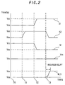
- the node N1 In the first and the second state where the main decoder signal S1 is at logic LOW, the node N1 is charged with the positive power supply Vcc, the pMOS transistor MP1 being ON. In the third state (HIGH, HIGH), the node N1 is discharged to the negative power supply Vss as illustrated in FIG. 2 through the third nMOS transistor MN3 becoming ON, in the NOR gate of FIG. 1. Therefore, when logic of the main decoder signal S1 and the pre-decoder signal S2 is changed from the third state (HIGH, HIGH) to the fourth state (HIGH, LOW) at the timing T3, the instantaneous discharge of the node N1 does not occur.
- the third nMOS transistor MN3 for discharging the node N1 when the first transistor MP1 is OFF, including charging with the sub-threshold current of the pMOS transistor MP1, the instantaneous discharge of the node N1 can be almost eliminated, enabling a sharp rising up of the selected word line WSL as illustrated in FIG. 2, in the embodiment.
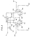
- a first pre-decoder signal S20 is supplied to the gate of the second pMOS transistor MP2 for controlling a first word line WL1, in FIG. 3.
- the first pMOS transistor MP1 When logic of the main decoder signal S1 is HIGH, the first pMOS transistor MP1 is OFF and the first and the fourth nMOS transistor MN1 and MN4 is ON, making both the first and the second word line WL1 and WL2 inactive.
- the third nMOS transistor MN3 becoming ON, it connects the node N1 to the low level power supply Vss, when the main decoder signal S1 turns to OFF, bypassing the floating charge of the node N1. Therefore, the instantaneous discharge of the node N1 can be prevented, in the same way with the embodiment of FIG. 1, with a half number of bypassing nMOS transistors MN3, compared to the embodiment of FIG. 1.
Landscapes
- Engineering & Computer Science (AREA)
- Microelectronics & Electronic Packaging (AREA)
- Computer Hardware Design (AREA)
- General Engineering & Computer Science (AREA)
- Physics & Mathematics (AREA)
- Computing Systems (AREA)
- Power Engineering (AREA)
- Mathematical Physics (AREA)
- Static Random-Access Memory (AREA)
- Dram (AREA)
- Read Only Memory (AREA)
- Semiconductor Memories (AREA)
- Logic Circuits (AREA)
Applications Claiming Priority (3)
| Application Number | Priority Date | Filing Date | Title |
|---|---|---|---|
| JP278934/96 | 1996-09-30 | ||
| JP27893496 | 1996-09-30 | ||
| JP8278934A JP2865080B2 (ja) | 1996-09-30 | 1996-09-30 | 半導体記憶装置 |
Publications (2)
| Publication Number | Publication Date |
|---|---|
| EP0833343A2 true EP0833343A2 (de) | 1998-04-01 |
| EP0833343A3 EP0833343A3 (de) | 2005-08-17 |
Family
ID=17604117
Family Applications (1)
| Application Number | Title | Priority Date | Filing Date |
|---|---|---|---|
| EP97116881A Withdrawn EP0833343A3 (de) | 1996-09-30 | 1997-09-29 | An einem Subdekodierer eines Halbleiterspeichers angekoppeltes NOR-Gatter |
Country Status (3)
| Country | Link |
|---|---|
| EP (1) | EP0833343A3 (de) |
| JP (1) | JP2865080B2 (de) |
| KR (1) | KR100300830B1 (de) |
Cited By (6)
| Publication number | Priority date | Publication date | Assignee | Title |
|---|---|---|---|---|
| EP1532632A4 (de) * | 2002-06-28 | 2005-09-21 | Rambus Inc | Speicherbaustein mit frühlese-nach-schreiboperation, system und verfahren |
| US7187572B2 (en) | 2002-06-28 | 2007-03-06 | Rambus Inc. | Early read after write operation memory device, system and method |
| US7380092B2 (en) | 2002-06-28 | 2008-05-27 | Rambus Inc. | Memory device and system having a variable depth write buffer and preload method |
| US7583559B2 (en) * | 2007-05-31 | 2009-09-01 | Intel Corporation | Two transistor wordline decoder output driver |
| US8072799B2 (en) | 2004-09-15 | 2011-12-06 | Renesas Electronics Corporation | Semiconductor integrated circuit device |
| RU2468510C1 (ru) * | 2011-09-16 | 2012-11-27 | Виктор Николаевич Мурашёв | Троичный к-моп-с логический элемент "или-не" |
Families Citing this family (2)
| Publication number | Priority date | Publication date | Assignee | Title |
|---|---|---|---|---|
| JP2002118176A (ja) * | 2000-10-05 | 2002-04-19 | Nec Corp | 半導体装置 |
| JP7374627B2 (ja) * | 2019-06-28 | 2023-11-07 | キヤノン株式会社 | デジタルアナログ変換回路、表示装置、電子機器 |
Family Cites Families (4)
| Publication number | Priority date | Publication date | Assignee | Title |
|---|---|---|---|---|
| US4618784A (en) * | 1985-01-28 | 1986-10-21 | International Business Machines Corporation | High-performance, high-density CMOS decoder/driver circuit |
| JPS62202399A (ja) * | 1985-10-04 | 1987-09-07 | Mitsubishi Electric Corp | 半導体メモリ |
| JPH02218096A (ja) * | 1989-02-17 | 1990-08-30 | Sharp Corp | 半導体メモリの行選択回路 |
| JPH0395797A (ja) * | 1989-09-08 | 1991-04-22 | Hitachi Ltd | 半導体集積回路装置 |
-
1996
- 1996-09-30 JP JP8278934A patent/JP2865080B2/ja not_active Expired - Fee Related
-
1997
- 1997-09-29 EP EP97116881A patent/EP0833343A3/de not_active Withdrawn
- 1997-09-29 KR KR1019970049544A patent/KR100300830B1/ko not_active Expired - Fee Related
Cited By (12)
| Publication number | Priority date | Publication date | Assignee | Title |
|---|---|---|---|---|
| EP1532632A4 (de) * | 2002-06-28 | 2005-09-21 | Rambus Inc | Speicherbaustein mit frühlese-nach-schreiboperation, system und verfahren |
| US7187572B2 (en) | 2002-06-28 | 2007-03-06 | Rambus Inc. | Early read after write operation memory device, system and method |
| US7369444B2 (en) | 2002-06-28 | 2008-05-06 | Rambus Inc. | Early read after write operation memory device, system and method |
| US7380092B2 (en) | 2002-06-28 | 2008-05-27 | Rambus Inc. | Memory device and system having a variable depth write buffer and preload method |
| US7848156B2 (en) | 2002-06-28 | 2010-12-07 | Rambus Inc. | Early read after write operation memory device, system and method |
| US8351281B2 (en) | 2002-06-28 | 2013-01-08 | Rambus Inc. | Early read after write operation memory device, system and method |
| US8665662B2 (en) | 2002-06-28 | 2014-03-04 | Rambus Inc. | Early read after write operation memory device, system and method |
| US8072799B2 (en) | 2004-09-15 | 2011-12-06 | Renesas Electronics Corporation | Semiconductor integrated circuit device |
| US8441843B2 (en) | 2004-09-15 | 2013-05-14 | Renesas Electronics Corporation | Semiconductor integrated circuit device |
| US9123435B2 (en) | 2004-09-15 | 2015-09-01 | Renesas Electronics Corporation | Semiconductor integrated circuit device |
| US7583559B2 (en) * | 2007-05-31 | 2009-09-01 | Intel Corporation | Two transistor wordline decoder output driver |
| RU2468510C1 (ru) * | 2011-09-16 | 2012-11-27 | Виктор Николаевич Мурашёв | Троичный к-моп-с логический элемент "или-не" |
Also Published As
| Publication number | Publication date |
|---|---|
| JP2865080B2 (ja) | 1999-03-08 |
| JPH10106268A (ja) | 1998-04-24 |
| KR100300830B1 (ko) | 2001-09-03 |
| EP0833343A3 (de) | 2005-08-17 |
| KR19980025099A (ko) | 1998-07-06 |
Similar Documents
| Publication | Publication Date | Title |
|---|---|---|
| KR0155078B1 (ko) | 강전계용의 mos 회로를 갖춘 반도체 회로 | |
| US6545525B2 (en) | Semiconductor device including interface circuit, logic circuit, and static memory array having transistors of various threshold voltages and being supplied with various supply voltages | |
| KR100297139B1 (ko) | 반도체 집적회로 | |
| EP0732701B1 (de) | Bitleitungsvorladungsstrombegrenzer für CMOS dynamische Speicher | |
| KR101269785B1 (ko) | SeOI상의 의사 인버터 회로 | |
| KR100363142B1 (ko) | 3상태논리게이트회로를갖는반도체집적회로 | |
| US5448518A (en) | Virtual ground type nonvolatile semiconductor memory device capable of simultaneously accessing two memory cells | |
| EP1255254A2 (de) | Wortleitungstreiber für eine Halbleiterspeicheranordnung | |
| US5157281A (en) | Level-shifter circuit for integrated circuits | |
| JPH0143464B2 (de) | ||
| EP0222472B1 (de) | Komplementäre Halbleitereinrichtung mit einem Substratspannungsgenerator | |
| JPH05182461A (ja) | 半導体メモリ装置 | |
| KR20030091828A (ko) | 반도체 기억 장치 | |
| KR0153847B1 (ko) | 반도체 기억장치 | |
| US6128230A (en) | Semiconductor memory with PN junction potential reduction in a writing mode | |
| EP0833343A2 (de) | An einem Subdekodierer eines Halbleiterspeichers angekoppeltes NOR-Gatter | |
| US5786719A (en) | Mode setting circuit and mode setting apparatus used to select a particular semiconductor function | |
| US20020141277A1 (en) | Semiconductor memory device with reduced its chip area and power consumption | |
| KR100223506B1 (ko) | 반도체 메모리 디바이스용 논리 회로 | |
| JP3047659B2 (ja) | 半導体集積回路 | |
| JP4075090B2 (ja) | 半導体装置 | |
| US5577003A (en) | Decoding circuit for use in semiconductor read only memory | |
| US6654309B1 (en) | Circuit and method for reducing voltage stress in a memory decoder | |
| US6570811B1 (en) | Writing operation control circuit and semiconductor memory using the same | |
| JP3553850B2 (ja) | 半導体メモリ装置 |
Legal Events
| Date | Code | Title | Description |
|---|---|---|---|
| PUAI | Public reference made under article 153(3) epc to a published international application that has entered the european phase |
Free format text: ORIGINAL CODE: 0009012 |
|
| AK | Designated contracting states |
Kind code of ref document: A2 Designated state(s): AT BE CH DE DK ES FI FR GB GR IE IT LI LU MC NL PT SE |
|
| RAP1 | Party data changed (applicant data changed or rights of an application transferred) |
Owner name: NEC ELECTRONICS CORPORATION Owner name: NEC CORPORATION |
|
| PUAL | Search report despatched |
Free format text: ORIGINAL CODE: 0009013 |
|
| AK | Designated contracting states |
Kind code of ref document: A3 Designated state(s): AT BE CH DE DK ES FI FR GB GR IE IT LI LU MC NL PT SE |
|
| 17P | Request for examination filed |
Effective date: 20050722 |
|
| AKX | Designation fees paid |
Designated state(s): DE FR GB |
|
| STAA | Information on the status of an ep patent application or granted ep patent |
Free format text: STATUS: THE APPLICATION HAS BEEN WITHDRAWN |
|
| 18W | Application withdrawn |
Effective date: 20060502 |