EP0833502A2 - Dispositif de prise d'image compact avec mémoire d'image locale - Google Patents
Dispositif de prise d'image compact avec mémoire d'image locale Download PDFInfo
- Publication number
- EP0833502A2 EP0833502A2 EP97202810A EP97202810A EP0833502A2 EP 0833502 A2 EP0833502 A2 EP 0833502A2 EP 97202810 A EP97202810 A EP 97202810A EP 97202810 A EP97202810 A EP 97202810A EP 0833502 A2 EP0833502 A2 EP 0833502A2
- Authority
- EP
- European Patent Office
- Prior art keywords
- array
- image
- lenslet
- radiation
- output
- Prior art date
- Legal status (The legal status is an assumption and is not a legal conclusion. Google has not performed a legal analysis and makes no representation as to the accuracy of the status listed.)
- Withdrawn
Links
- 230000015654 memory Effects 0.000 claims abstract description 27
- 230000005855 radiation Effects 0.000 claims abstract description 26
- 230000003287 optical effect Effects 0.000 claims abstract description 21
- 238000005070 sampling Methods 0.000 claims abstract description 10
- 230000002596 correlated effect Effects 0.000 claims abstract description 9
- 230000006870 function Effects 0.000 claims description 14
- 230000000875 corresponding effect Effects 0.000 claims description 6
- 238000006073 displacement reaction Methods 0.000 claims description 4
- 230000001276 controlling effect Effects 0.000 claims 1
- 230000035945 sensitivity Effects 0.000 description 7
- 230000000694 effects Effects 0.000 description 6
- 230000008901 benefit Effects 0.000 description 5
- 230000009977 dual effect Effects 0.000 description 5
- 230000007423 decrease Effects 0.000 description 4
- 238000010586 diagram Methods 0.000 description 4
- 238000010348 incorporation Methods 0.000 description 4
- 238000012546 transfer Methods 0.000 description 4
- 238000003491 array Methods 0.000 description 3
- 230000010354 integration Effects 0.000 description 3
- 238000000034 method Methods 0.000 description 3
- 238000012545 processing Methods 0.000 description 3
- 230000003321 amplification Effects 0.000 description 2
- 239000011521 glass Substances 0.000 description 2
- 238000003199 nucleic acid amplification method Methods 0.000 description 2
- 230000009467 reduction Effects 0.000 description 2
- 125000006850 spacer group Chemical group 0.000 description 2
- 239000004593 Epoxy Substances 0.000 description 1
- 238000004458 analytical method Methods 0.000 description 1
- 230000005540 biological transmission Effects 0.000 description 1
- 239000003990 capacitor Substances 0.000 description 1
- 230000003247 decreasing effect Effects 0.000 description 1
- 230000000593 degrading effect Effects 0.000 description 1
- 238000001514 detection method Methods 0.000 description 1
- 230000008030 elimination Effects 0.000 description 1
- 238000003379 elimination reaction Methods 0.000 description 1
- 238000005286 illumination Methods 0.000 description 1
- 238000003384 imaging method Methods 0.000 description 1
- 230000006872 improvement Effects 0.000 description 1
- 238000002347 injection Methods 0.000 description 1
- 239000007924 injection Substances 0.000 description 1
- 238000012886 linear function Methods 0.000 description 1
- 239000000463 material Substances 0.000 description 1
- 238000012986 modification Methods 0.000 description 1
- 230000004048 modification Effects 0.000 description 1
- 239000002991 molded plastic Substances 0.000 description 1
- 238000012544 monitoring process Methods 0.000 description 1
- 229920002120 photoresistant polymer Polymers 0.000 description 1
- 239000010453 quartz Substances 0.000 description 1
- 238000012552 review Methods 0.000 description 1
- 239000004065 semiconductor Substances 0.000 description 1
- 229910052710 silicon Inorganic materials 0.000 description 1
- 239000010703 silicon Substances 0.000 description 1
- VYPSYNLAJGMNEJ-UHFFFAOYSA-N silicon dioxide Inorganic materials O=[Si]=O VYPSYNLAJGMNEJ-UHFFFAOYSA-N 0.000 description 1
- 239000000758 substrate Substances 0.000 description 1
Images


Classifications
-
- H—ELECTRICITY
- H10—SEMICONDUCTOR DEVICES; ELECTRIC SOLID-STATE DEVICES NOT OTHERWISE PROVIDED FOR
- H10F—INORGANIC SEMICONDUCTOR DEVICES SENSITIVE TO INFRARED RADIATION, LIGHT, ELECTROMAGNETIC RADIATION OF SHORTER WAVELENGTH OR CORPUSCULAR RADIATION
- H10F39/00—Integrated devices, or assemblies of multiple devices, comprising at least one element covered by group H10F30/00, e.g. radiation detectors comprising photodiode arrays
- H10F39/80—Constructional details of image sensors
- H10F39/806—Optical elements or arrangements associated with the image sensors
- H10F39/8063—Microlenses
-
- H—ELECTRICITY
- H04—ELECTRIC COMMUNICATION TECHNIQUE
- H04N—PICTORIAL COMMUNICATION, e.g. TELEVISION
- H04N23/00—Cameras or camera modules comprising electronic image sensors; Control thereof
- H04N23/50—Constructional details
- H04N23/55—Optical parts specially adapted for electronic image sensors; Mounting thereof
-
- H—ELECTRICITY
- H04—ELECTRIC COMMUNICATION TECHNIQUE
- H04N—PICTORIAL COMMUNICATION, e.g. TELEVISION
- H04N25/00—Circuitry of solid-state image sensors [SSIS]; Control thereof
- H04N25/40—Extracting pixel data from image sensors by controlling scanning circuits, e.g. by modifying the number of pixels sampled or to be sampled
- H04N25/41—Extracting pixel data from a plurality of image sensors simultaneously picking up an image, e.g. for increasing the field of view by combining the outputs of a plurality of sensors
-
- H—ELECTRICITY
- H04—ELECTRIC COMMUNICATION TECHNIQUE
- H04N—PICTORIAL COMMUNICATION, e.g. TELEVISION
- H04N25/00—Circuitry of solid-state image sensors [SSIS]; Control thereof
- H04N25/70—SSIS architectures; Circuits associated therewith
-
- H—ELECTRICITY
- H04—ELECTRIC COMMUNICATION TECHNIQUE
- H04N—PICTORIAL COMMUNICATION, e.g. TELEVISION
- H04N25/00—Circuitry of solid-state image sensors [SSIS]; Control thereof
- H04N25/70—SSIS architectures; Circuits associated therewith
- H04N25/76—Addressed sensors, e.g. MOS or CMOS sensors
- H04N25/766—Addressed sensors, e.g. MOS or CMOS sensors comprising control or output lines used for a plurality of functions, e.g. for pixel output, driving, reset or power
-
- H—ELECTRICITY
- H04—ELECTRIC COMMUNICATION TECHNIQUE
- H04N—PICTORIAL COMMUNICATION, e.g. TELEVISION
- H04N25/00—Circuitry of solid-state image sensors [SSIS]; Control thereof
- H04N25/70—SSIS architectures; Circuits associated therewith
- H04N25/76—Addressed sensors, e.g. MOS or CMOS sensors
- H04N25/77—Pixel circuitry, e.g. memories, A/D converters, pixel amplifiers, shared circuits or shared components
-
- H—ELECTRICITY
- H04—ELECTRIC COMMUNICATION TECHNIQUE
- H04N—PICTORIAL COMMUNICATION, e.g. TELEVISION
- H04N25/00—Circuitry of solid-state image sensors [SSIS]; Control thereof
- H04N25/70—SSIS architectures; Circuits associated therewith
- H04N25/76—Addressed sensors, e.g. MOS or CMOS sensors
- H04N25/77—Pixel circuitry, e.g. memories, A/D converters, pixel amplifiers, shared circuits or shared components
- H04N25/771—Pixel circuitry, e.g. memories, A/D converters, pixel amplifiers, shared circuits or shared components comprising storage means other than floating diffusion
-
- G—PHYSICS
- G02—OPTICS
- G02B—OPTICAL ELEMENTS, SYSTEMS OR APPARATUS
- G02B3/00—Simple or compound lenses
- G02B3/0006—Arrays
- G02B3/0037—Arrays characterized by the distribution or form of lenses
- G02B3/0043—Inhomogeneous or irregular arrays, e.g. varying shape, size, height
Definitions
- This invention relates generally to the field of image capture devices and more particularly to an improvement that integrates analog and digital circuits and image memory into the areas between the individual photodetectors that form the image capture device and to their combination formed as an optical array camera.
- Fossum does not however allow for an increase in the overall sensitivity of the photosensor (CCD detector) elements, nor does it envision the utilization of an array optic type structure to form an image of different segments of a field of view, although the patent does disclose the use of a lens array for concentrating light on the active pixel.
- Fossum does not include means for adjusting the overall exposure level of the pixel internal to the unit cell of the detector array.
- Fossum is also performing most of the signal processing in a voltage amplification mode, whereas the present invention utilizes the advantages of a current mode of signal processing.
- the present invention provides for the digitization and storage of the digital image data at each photosensor site.
- Yoshimoto's invention The purpose of Yoshimoto's invention is to allow the utilization of received photocurrents with a large dynamic range by multiplying the input current by an adjustable ratio, where the multiple current ratios are selected through a switchable network of differential amplifiers.
- Yoshimoto's invention is not related to the field of array image sensors and requires the use of a switchable array of differencing amplifiers.
- Yoshimoto's invention does not integrate the current from the photosensor and the current is continuously generated by received light from the laser light emitted by the optical disk head. Therefore, the sensor is not exposed to an image with its sensed signals being integrated by analog and digital signal processing electronics, as in the current invention, but is rather used in a continuous optical disk position monitoring mode.
- Yoshimoto does not utilize dual slope correlated double sampling for noise reduction as disclosed in the present invention.
- Yoshimoto does not make any mention of the use of array optics with a field of view which varies as a function of radial position in the sensor array.
- a compact image capture device comprising an array of spaced apart radiation sensors for providing output signals that are a function of the incident radiation from an image onto each radiation sensor; array electronics dispersed in the spaces between the spaced apart radiation sensors for receiving the provided output signals so as to amplify, digitize, and store the provided output signals to facilitate image capture; and a lens array positioned so as to focus the radiation of an image to be captured onto said radiation sensors.
- the present invention has the advantages of increased signal current produced by a combination of current mirrors positioned in close physical proximity to associated arrayed photodetectors where the increased signal current represents an increase in sensitivity for the photosensor array.
- This increased sensitivity allows for the use of shorter exposure times, or the use of optics with smaller numerical apertures when the photosensor array is used in a camera.
- the use of lower numerical aperture optics (higher F/#'s) in a camera allows for greater depth of focus, easier alignment of optics and photosensor and in general decreased system costs.
- a unit pixel subassembly 10 forms part of a camera's photosensor array 100 (see array of Fig. 4).
- the unit pixel subassembly 10 is comprised of a photodetector 20, which may be, for example, a CCD device and/or a photodiode.
- the output 22 of the photodetector 20 is connected to a transfer gate 24, a reset gate 26, and a multiplying current mirror 30A.
- the transfer gate 24 allows the charge, accumulated by the photodetector 20 during the exposure period, to be transferred to the multiplying current mirror 30A at the desired time.
- the reset gate 26 allows for the emptying of the photodetector's 20 accumulated charge from the previously completed exposure.
- the output from the photodetector 20 is integrated for a time equivalent to the previous exposure time so as to cancel dark current and noise.
- This cancellation occurs within a correlated double sampling circuit (CDS) 40.
- the integrated signal from the CDS circuit 40 is digitized by an analog-to-digital converter 56 and the resulting digital value is stored in a non-volatile memory 58 which may be a SRAM memory.
- the digital value can be output to the main data bus 50 by accessing the unit pixel subassemby(s) through row and column address decoders.
- the image data may be stored at site and/or downloaded after each capture.
- the photosensor array 100 is then ready for exposure to a new image.
- the output of the current mirror 30A is a multiple of the current produced by the photodetector 20.
- the current multiplying effect is traditionally accomplished either by connecting the bases or gates of the transistors 32 1 through 32 n in parallel with each other or by making the emitter (or source) areas larger by an integral multiple of the emitter area of an input side transistor 34.
- Current mirrors of this type operate on the principle that the emitter base voltage (or the gate source voltage) for all the transistors in the current mirror are the same so that each of the collector (drain) currents is the same, and therefore the sum of the currents from the output side T o is a multiple of either the number of transistors in the output side or the ratio of the area.
- the output of the current mirror 30A is switched between two current amplifiers, amplifiers 42 and 44, with gains of +1 and -1, respectively.
- amplifiers 42 and 44 When the photodetector 20 is receiving incident light its amplified current is switched through the +1 gain of amplifier 42 into an integrating amplifier 46 for a given amount of time and then after the shutter is closed the current is integrated through the -1 gain of amplifier 44 for an equal amount of time.
- This operation is known as dual slope, correlated double sampling, and it eliminates the effects of dark current and KTC noise. It differs from dual sample CDS in that the signal is switched through two different amplifiers depending on whether the signal represents the image data or the background data wherever dual time CDS uses the same amplification chain. Correlated double sampling also reduces Johnson noise, flicker noise, and 1/f noise.
- a similar effect can be achieved by integrating the current from an opaquely masked photodetector through the -1 gain of amplifier 44.
- Using an opaquely masked photodetector adjacent to the active photodetector 20 allows the correlated double sampling technique to be implemented in parallel and decreases readout time.
- the integration of the outputs of the current amplifiers 42 and 44 occurs simultaneously, thus eliminating the need to wait for two integration periods to have output data.
- separate photodetectors are used, small differences in dark current and noise can arise between them.
- the integrated signal from the photosensors is then digitized by an analog-to-digital converter (ADC) circuit 56.
- ADC analog-to-digital converter
- the output of the ADC is stored in the memory cells 58.
- there is only one memory cell at each unit pixel subassembly site it is also possible to locate multiple memory cells at each site which allows for the storage of multiple images on the photosensor array 100. This essentially allows the compact photosensor array to act as an optic array camera 200, complete with an array lens 210 (see Fig. 5).
- the digital intensity data is accessed by strobing the memory cells 58 via row and column address decoders, in order to send data to the data bus 50.
- the incorporation of the row and column address data lines allows for addressing of subsections of the photosensitive array for more rapid image readout in a specific area of interest in the image. This is useful in digital cameras which monitor a scene and are only interested in updating the section of the image associated with moving objects.
- a current mirror circuit 30B that may be substituted for the current mirror 30A, provides a second variant of the current mirror function by utilizing an output transistor T o emitter or source whose area is n times the area of the emitter or source of the input transistor T i . This forms a smaller circuit which in turn allocates more area to the photodetector 20.
- Current mirror 30B would be substituted for the current mirror 30A at the connection point marked with a circled A.
- Fig. 3 illustrates another variant of current mirror labeled 30C that is connectable to the unit pixel subassembly 10 of Fig. 1 at the A labeled point marked with a circle in place of either current mirrors 30A or 30B.
- the current mirror 30C achieves current multiplication by biasing the emitter base (or gate source) voltage higher on the input side of the current mirror than on the output side. This, more specifically, is accomplished by adjusting the value of R1 and R2. Alternately, a diode junction can be substituted into the emitter or source of the input side of the current mirror 30C in order to provide a fixed voltage bias.
- photosensor array 100 contains unused areas at each photodetector site due to the use of an array optic with a variable field of view. It is within these areas that the circuits 30A, B, or C, and circuit 40, as well as the analog-to-digital converter 56 and memory cells 58, are located. As previously mentioned, the placement of these circuits in close proximity to their associated photodetectors 20 makes a more efficient photosensor array and reduces the need for external support circuitry.
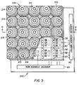
- the photosensor array 100 is shown in a block layout form for ease of understanding.
- Each unit pixel subassembly is connected to a row address decoder 60 and a column address decoder 62.
- data from a subsection of an array can be accessed by using only those addresses that represent the location of data of interest. In this fashion segments of a captured image may be clocked out more rapidly in order to view areas that are capturing rapid scene changes while sampling less active areas less frequently.
- the length of the addresses are increased accordingly to allow individual access to each of the multiple image data words (pixel image data).
- Fig. 5 illustrates an optic array camera 200 incorporating the photosensor array 100 and a lenslet array 210.
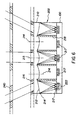
- Fig. 6 illustrates a cross-section of the optic array camera, taken along the section lines 6-6, in Fig. 5.
- the optic array camera 200 is formed with an array 210 of achromatized refractive/diffractive lenslets 212 or refractive lenslets which are centered over photosensitive sites 217.
- the array of lenslets 210 replaces the typical single round lenses that are spaced along one central axis in a camera. To be observed in Fig.
- each lenslet 212 is displaced relative to the fixed sensor-to-sensor distance as a function of its radial distance from the optical axis 213 of the central lenslet which is at the physical center of the array shown.
- the lines 215, appearing around the mechanical optical axis 214 of each lenslet 212, are topographical lines indicating changes in height of the lenslet's surface.
- An opaque mask 216 covers the areas between the lenslets 212 to prevent light from reaching the photodetectors (photosensor) other than by passing through a lenslet.
- the array depicted in Fig. 6 represents only a small portion of an array that is used in an actual camera.
- a typical implementation could consist of 480 x 640 (or more) pixels with 3 pixels per lens.
- Other configurations of the lenslets may be used such as forming the outer periphery of each lenslet 212 as a square, hexagon, or circle, without detracting from the invention.
- the optical axis 214 of the lenslets 212 in the lens array 100 are located at a distance which becomes progressively larger than the center-to-center distance of the pixels in the array.
- the displacement of the lenslets optical axis 214 increases radially from the center of the array. Decentering a lens element tends to bend rays from off-axis field angles into the center of the lens groups field of view.
- the optical axis of the lens element By moving the optical axis of the lens element further out radially with increasing distance from the center of the array, the angular location of an object at the center of the field of view for a given lenslet/photodetector pair originates from increasingly off-axis segments of the total field of view.
- the required decenter, for an array element of focal length Fl i necessary to deflect a ray from the desired field angle into the center of the array element's field stop can be determined from the paraxial ray tracing equations.
- the decenter necessary for a given element is approximately a linear function of the element's radial distance from the system's optical axis.
- the lenslet array 210 is positioned over the photosensor array 100 of grouped photosensors 222.
- Each photosensor group 222 is located at an associated photosensitive site 217.
- Each group of photosensors 222 is formed with red (R), green (G), and blue (B) sensors.
- the number of photosensitive sites 217 corresponds in number to at least the number of lenslets 212 in the lenslet array 210.
- the lenslet array 210 is maintained a distance apart from the surfaces of the photosensors by spacers 218 that serve the additional function of being light baffles.
- the opaque masks 216 on the lenslet array 210 combined with a field stop aperture plate 240 limit the field of view of any particular photosensor so that it does not overlap the field of view of its neighbors by a large amount.
- the aperture plate 240 is positioned approximately 0.5mm to 2.0mm from the surface of the lenslet array 210.
- the aperture plate 240 may be a layer of clear glass having a photoresist mask pattern formed on one of it's surfaces.
- the center of the apertures in the aperture plate 240 are aligned to the center of the field of view of a corresponding lenslet.
- the spacing of the mechanical optical centers 214 increases as a function of each lenslet's radial position radially from the center of the array causing the aperture plate 240 to be slightly larger than the associated lenslet array 210.
- the combination of the opaque areas 216 with the aperture plate 240 and a given lenslet focal length determines the field of view for a photosensitive site 217.
- the lenslet array 210 can be formed of etched quartz, or an epoxy replica on a glass substrate or can be injection molded plastic.
- the lenslets 212 combined with the appropriate field stop aperture plate 240, form images of a small segment of the field of view on each photosensitive site 217.
- the lenslets 212 By forming the lenslets 212 with decentrations of the mechanical optical axis 214, which increase radially across the lenslet array, the angle which the axial ray incident on any particular lenslet makes with the surface normal to the plane of the lenslet array 210 will increase as a function of the particular lenslet's radial position on the array. Therefore, by appropriately forming the decenters of each lenslet each photosensitive site 217 will view a different segment of a scene (image). Since each photosensor group 222 has its own lenslet there is no need to reinvert the image with a relay lens.
- any camera system incorporating the present invention, can be extremely compact and flat due to the integration of the above described circuitry which allows for the elimination of support circuit boards which in turn allows for a further decrease in the size of the camera.
- the camera can work in black and white or in color if three unit pixel subassemblies with color filters are formed at each pixel site 217 to pass only assigned frequencies of incident radiation.
- An array of aspheric lenslets can also be used to form images on the photosensor array 100.
- the aforementioned embodiment does not correct for the variation in focal length as a function of wavelength since the lenslet is formed from a single refractive material, therefore the spot size of the incident light varies as a function of color.
- each lenslet's F/# allows for the reduction of the center-to-center spacing between array elements, since, for a given F/# and detector sensitivity a specific photocurrent is generated.
- an array optic camera is formed with 780 by 640 pixels the length of the long dimension of the array would be 32.5 mm, assuming 3 color pixels (photosensors) at each photosite. This would require a large area of silicon per photosensor array, which would increase part costs and result in lower yields of photosensors from a given wafer size.
- the lenslet diameters can be reduced by 4x to 65 ⁇ m and the length of the array will be reduced to 8.125 mm, resulting in higher photosensor yields and lower part costs.
- the array optic camera can utilize this technique with no decrease in usable photosensitive surface area since the space between photosites is not utilized for light detection.
- the area between photosensors can be minimized to allow only the necessary support circuitry. For instance, if the spacing between photosensor is 65 ⁇ m and the single color photosensor size is a square, 5 to 10 ⁇ m on a side there is 4225 ⁇ m 2 in a unit cell and only 75 to 300 ⁇ m 2 surface area associated with the three color photosensor's active area. Therefore, the area between pixels is 56 to 14 times as large as the photosensor. This extra area allows for the incorporation of the analog circuitry, the ADC and from 1 to n non-volatile memory cells at each photosite. The larger the number of memory cells, the larger the number of images that can be stored at the photosite.
- DRAM memory allows for storing image data even when the power to the camera is turned off. It is also possible to use DRAM memory at the photosites given that it is acceptable to include refresh circuitry. DRAM memory can be constructed using less surface area which allows for either smaller distance between photosites or storage of more image data.
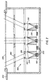
- Fig. 7 illustrates the optic array camera 200 of Fig. 6 positioned in a light tight housing 252 that is exposed to an image via a mechanical shutter 250.
- the mechanical shutter may be any of the typical shutters used in a film type camera.
- the advantage to the optic array camera 200 of Fig. 6 is that no mechanical shutter is required; the photosensors 222 are turned on " or active to capture light from the image focused onto the photosensor array 100. In the Fig. 7 embodiment the photosensors 222 are turned on " generally when camera power is on and image capture occurs when the shutter 250 is activated.
Landscapes
- Engineering & Computer Science (AREA)
- Multimedia (AREA)
- Signal Processing (AREA)
- Transforming Light Signals Into Electric Signals (AREA)
- Solid State Image Pick-Up Elements (AREA)
Applications Claiming Priority (2)
| Application Number | Priority Date | Filing Date | Title |
|---|---|---|---|
| US72028296A | 1996-09-26 | 1996-09-26 | |
| US720282 | 1996-09-26 |
Publications (2)
| Publication Number | Publication Date |
|---|---|
| EP0833502A2 true EP0833502A2 (fr) | 1998-04-01 |
| EP0833502A3 EP0833502A3 (fr) | 2000-01-05 |
Family
ID=24893418
Family Applications (1)
| Application Number | Title | Priority Date | Filing Date |
|---|---|---|---|
| EP97202810A Withdrawn EP0833502A3 (fr) | 1996-09-26 | 1997-09-13 | Dispositif de prise d'image compact avec mémoire d'image locale |
Country Status (2)
| Country | Link |
|---|---|
| EP (1) | EP0833502A3 (fr) |
| JP (1) | JPH10112823A (fr) |
Cited By (8)
| Publication number | Priority date | Publication date | Assignee | Title |
|---|---|---|---|---|
| EP0893915A3 (fr) * | 1997-06-25 | 2000-01-05 | Eastman Kodak Company | Capteur d'image compact attaché à un dispositif d'affichage |
| EP0840502A3 (fr) * | 1996-11-04 | 2000-01-05 | Eastman Kodak Company | Caméra digitale compacte avec champs de vue segmentés |
| EP1225758A3 (fr) * | 2001-01-03 | 2004-03-24 | Pixim, Inc. | Matrice de capteurs CMOS avec un interface mémoire |
| EP1182865A3 (fr) * | 2000-08-15 | 2004-08-11 | Pixim, Inc | Circuit et méthode pour réarranger les pixels dans un tableau de valeurs de détecteur de pixels |
| US6831684B1 (en) | 2000-05-09 | 2004-12-14 | Pixim, Inc. | Circuit and method for pixel rearrangement in a digital pixel sensor readout |
| KR100778824B1 (ko) * | 2000-02-22 | 2007-11-22 | 픽심 인코포레이티드 | 시간지수 방법을 통한 다중 샘플링 이미지 센서 및 이미지 센서의 동적 영역을 확장하는 방법 및 이를 이용한 장치 |
| EP2518770A1 (fr) * | 2011-04-28 | 2012-10-31 | Commissariat à l'Énergie Atomique et aux Énergies Alternatives | Dispositif imageur destiné à evaluer des distances d'éléments dans une image |
| WO2014057106A1 (fr) * | 2012-10-12 | 2014-04-17 | Fraunhofer-Gesellschaft zur Förderung der angewandten Forschung e.V. | Capteur d'image |
Families Citing this family (1)
| Publication number | Priority date | Publication date | Assignee | Title |
|---|---|---|---|---|
| KR100715970B1 (ko) * | 2001-03-08 | 2007-05-08 | 삼성전자주식회사 | 메모리 모듈 |
Family Cites Families (4)
| Publication number | Priority date | Publication date | Assignee | Title |
|---|---|---|---|---|
| US5471515A (en) * | 1994-01-28 | 1995-11-28 | California Institute Of Technology | Active pixel sensor with intra-pixel charge transfer |
| US5461425A (en) * | 1994-02-15 | 1995-10-24 | Stanford University | CMOS image sensor with pixel level A/D conversion |
| JPH08107194A (ja) * | 1994-10-03 | 1996-04-23 | Fuji Photo Optical Co Ltd | 固体撮像装置 |
| US6141048A (en) * | 1996-08-19 | 2000-10-31 | Eastman Kodak Company | Compact image capture device |
-
1997
- 1997-09-13 EP EP97202810A patent/EP0833502A3/fr not_active Withdrawn
- 1997-09-16 JP JP9250650A patent/JPH10112823A/ja active Pending
Cited By (13)
| Publication number | Priority date | Publication date | Assignee | Title |
|---|---|---|---|---|
| EP0840502A3 (fr) * | 1996-11-04 | 2000-01-05 | Eastman Kodak Company | Caméra digitale compacte avec champs de vue segmentés |
| US6137535A (en) * | 1996-11-04 | 2000-10-24 | Eastman Kodak Company | Compact digital camera with segmented fields of view |
| EP0893915A3 (fr) * | 1997-06-25 | 2000-01-05 | Eastman Kodak Company | Capteur d'image compact attaché à un dispositif d'affichage |
| KR100778824B1 (ko) * | 2000-02-22 | 2007-11-22 | 픽심 인코포레이티드 | 시간지수 방법을 통한 다중 샘플링 이미지 센서 및 이미지 센서의 동적 영역을 확장하는 방법 및 이를 이용한 장치 |
| US6831684B1 (en) | 2000-05-09 | 2004-12-14 | Pixim, Inc. | Circuit and method for pixel rearrangement in a digital pixel sensor readout |
| US6985181B2 (en) | 2000-05-09 | 2006-01-10 | Pixim, Inc. | CMOS sensor array with a memory interface |
| EP1182865A3 (fr) * | 2000-08-15 | 2004-08-11 | Pixim, Inc | Circuit et méthode pour réarranger les pixels dans un tableau de valeurs de détecteur de pixels |
| EP1225758A3 (fr) * | 2001-01-03 | 2004-03-24 | Pixim, Inc. | Matrice de capteurs CMOS avec un interface mémoire |
| CN1312776C (zh) * | 2001-01-03 | 2007-04-25 | 匹克希姆公司 | 具有存储器接口的cmos传感器阵列 |
| EP2518770A1 (fr) * | 2011-04-28 | 2012-10-31 | Commissariat à l'Énergie Atomique et aux Énergies Alternatives | Dispositif imageur destiné à evaluer des distances d'éléments dans une image |
| FR2974669A1 (fr) * | 2011-04-28 | 2012-11-02 | Commissariat Energie Atomique | Dispositif imageur destine a evaluer des distances d'elements dans une image |
| US8780257B2 (en) | 2011-04-28 | 2014-07-15 | Commissariat à l'énergie atmoque et aux énergies alternatives | Imager device for evaluating distances of elements in an image |
| WO2014057106A1 (fr) * | 2012-10-12 | 2014-04-17 | Fraunhofer-Gesellschaft zur Förderung der angewandten Forschung e.V. | Capteur d'image |
Also Published As
| Publication number | Publication date |
|---|---|
| EP0833502A3 (fr) | 2000-01-05 |
| JPH10112823A (ja) | 1998-04-28 |
Similar Documents
| Publication | Publication Date | Title |
|---|---|---|
| US6141048A (en) | Compact image capture device | |
| US6137535A (en) | Compact digital camera with segmented fields of view | |
| US10935930B2 (en) | Method, apparatus and system providing holographic layer as micro-lens and color filter array in an imager | |
| CN100499141C (zh) | 固体摄像装置 | |
| US6750437B2 (en) | Image pickup apparatus that suitably adjusts a focus | |
| EP0893915A2 (fr) | Capteur d'image compact attaché à un dispositif d'affichage | |
| US6765617B1 (en) | Optoelectronic camera and method for image formatting in the same | |
| JP4388226B2 (ja) | センサ装置 | |
| US7154548B2 (en) | Multiplexed and pipelined column buffer for use with an array of photo sensors | |
| KR20010034571A (ko) | 능동 선형 센서 | |
| CN113810635A (zh) | 高动态范围cmos图像传感器设计 | |
| EP1302986A1 (fr) | Photodétecteur à large gamme dynamique et de température de fonctionnement accrue | |
| EP0833502A2 (fr) | Dispositif de prise d'image compact avec mémoire d'image locale | |
| JP2024109935A (ja) | 撮像素子 | |
| CN110352489B (zh) | 用于cmos成像传感器的自动对焦系统 | |
| WO2020079960A1 (fr) | Dispositif d'imagerie et dispositif d'imagerie à semi-conducteurs | |
| EP2061235B1 (fr) | Procédé de correction de sensibilité et dispositif imageur | |
| CN100498496C (zh) | 测光测距用固体摄像装置以及使用了该装置的摄像装置 | |
| Monteiro et al. | Fast Hartmann-Shack wavefront sensors manufactured in standard CMOS technology | |
| CA2301345A1 (fr) | Prise de cliche | |
| JP2004191630A (ja) | 撮像装置 | |
| JP2004264451A (ja) | 測光測距用固体撮像装置 | |
| WO2023013261A1 (fr) | Élément d'imagerie à semi-conducteurs et appareil électronique | |
| Chatard et al. | Impact Of Focal Plane Technologies On IR System Design | |
| JPH11307751A (ja) | 固体撮像装置 |
Legal Events
| Date | Code | Title | Description |
|---|---|---|---|
| PUAI | Public reference made under article 153(3) epc to a published international application that has entered the european phase |
Free format text: ORIGINAL CODE: 0009012 |
|
| AK | Designated contracting states |
Kind code of ref document: A2 Designated state(s): AT BE CH DE DK ES FI FR GB GR IE IT LI LU MC NL PT SE |
|
| PUAL | Search report despatched |
Free format text: ORIGINAL CODE: 0009013 |
|
| AK | Designated contracting states |
Kind code of ref document: A3 Designated state(s): AT BE CH DE DK ES FI FR GB GR IE IT LI LU MC NL PT SE |
|
| RIC1 | Information provided on ipc code assigned before grant |
Free format text: 7H 04N 3/15 A, 7H 04N 5/335 B, 7H 04N 5/225 B |
|
| STAA | Information on the status of an ep patent application or granted ep patent |
Free format text: STATUS: THE APPLICATION IS DEEMED TO BE WITHDRAWN |
|
| AKX | Designation fees paid | ||
| REG | Reference to a national code |
Ref country code: DE Ref legal event code: 8566 |
|
| 18D | Application deemed to be withdrawn |
Effective date: 19991001 |