WO2020079960A1 - Dispositif d'imagerie et dispositif d'imagerie à semi-conducteurs - Google Patents
Dispositif d'imagerie et dispositif d'imagerie à semi-conducteurs Download PDFInfo
- Publication number
- WO2020079960A1 WO2020079960A1 PCT/JP2019/033232 JP2019033232W WO2020079960A1 WO 2020079960 A1 WO2020079960 A1 WO 2020079960A1 JP 2019033232 W JP2019033232 W JP 2019033232W WO 2020079960 A1 WO2020079960 A1 WO 2020079960A1
- Authority
- WO
- WIPO (PCT)
- Prior art keywords
- light
- light receiving
- incident
- image sensor
- unit
- Prior art date
- Legal status (The legal status is an assumption and is not a legal conclusion. Google has not performed a legal analysis and makes no representation as to the accuracy of the status listed.)
- Ceased
Links
Images


Classifications
-
- H—ELECTRICITY
- H10—SEMICONDUCTOR DEVICES; ELECTRIC SOLID-STATE DEVICES NOT OTHERWISE PROVIDED FOR
- H10F—INORGANIC SEMICONDUCTOR DEVICES SENSITIVE TO INFRARED RADIATION, LIGHT, ELECTROMAGNETIC RADIATION OF SHORTER WAVELENGTH OR CORPUSCULAR RADIATION
- H10F39/00—Integrated devices, or assemblies of multiple devices, comprising at least one element covered by group H10F30/00, e.g. radiation detectors comprising photodiode arrays
- H10F39/80—Constructional details of image sensors
- H10F39/804—Containers or encapsulations
-
- G—PHYSICS
- G01—MEASURING; TESTING
- G01J—MEASUREMENT OF INTENSITY, VELOCITY, SPECTRAL CONTENT, POLARISATION, PHASE OR PULSE CHARACTERISTICS OF INFRARED, VISIBLE OR ULTRAVIOLET LIGHT; COLORIMETRY; RADIATION PYROMETRY
- G01J1/00—Photometry, e.g. photographic exposure meter
- G01J1/02—Details
- G01J1/0214—Constructional arrangements for removing stray light
-
- G—PHYSICS
- G01—MEASURING; TESTING
- G01J—MEASUREMENT OF INTENSITY, VELOCITY, SPECTRAL CONTENT, POLARISATION, PHASE OR PULSE CHARACTERISTICS OF INFRARED, VISIBLE OR ULTRAVIOLET LIGHT; COLORIMETRY; RADIATION PYROMETRY
- G01J1/00—Photometry, e.g. photographic exposure meter
- G01J1/02—Details
- G01J1/04—Optical or mechanical part supplementary adjustable parts
- G01J1/0407—Optical elements not provided otherwise, e.g. manifolds, windows, holograms, gratings
- G01J1/0474—Diffusers
-
- G—PHYSICS
- G01—MEASURING; TESTING
- G01J—MEASUREMENT OF INTENSITY, VELOCITY, SPECTRAL CONTENT, POLARISATION, PHASE OR PULSE CHARACTERISTICS OF INFRARED, VISIBLE OR ULTRAVIOLET LIGHT; COLORIMETRY; RADIATION PYROMETRY
- G01J5/00—Radiation pyrometry, e.g. infrared or optical thermometry
- G01J5/02—Constructional details
- G01J5/06—Arrangements for eliminating effects of disturbing radiation; Arrangements for compensating changes in sensitivity
-
- G—PHYSICS
- G01—MEASURING; TESTING
- G01J—MEASUREMENT OF INTENSITY, VELOCITY, SPECTRAL CONTENT, POLARISATION, PHASE OR PULSE CHARACTERISTICS OF INFRARED, VISIBLE OR ULTRAVIOLET LIGHT; COLORIMETRY; RADIATION PYROMETRY
- G01J5/00—Radiation pyrometry, e.g. infrared or optical thermometry
- G01J5/02—Constructional details
- G01J5/08—Optical arrangements
- G01J5/0878—Diffusers
-
- G—PHYSICS
- G02—OPTICS
- G02B—OPTICAL ELEMENTS, SYSTEMS OR APPARATUS
- G02B27/00—Optical systems or apparatus not provided for by any of the groups G02B1/00 - G02B26/00, G02B30/00
- G02B27/0018—Optical systems or apparatus not provided for by any of the groups G02B1/00 - G02B26/00, G02B30/00 with means for preventing ghost images
-
- G—PHYSICS
- G02—OPTICS
- G02B—OPTICAL ELEMENTS, SYSTEMS OR APPARATUS
- G02B5/00—Optical elements other than lenses
- G02B5/02—Diffusing elements; Afocal elements
- G02B5/0273—Diffusing elements; Afocal elements characterized by the use
- G02B5/0278—Diffusing elements; Afocal elements characterized by the use used in transmission
-
- H—ELECTRICITY
- H04—ELECTRIC COMMUNICATION TECHNIQUE
- H04N—PICTORIAL COMMUNICATION, e.g. TELEVISION
- H04N23/00—Cameras or camera modules comprising electronic image sensors; Control thereof
- H04N23/20—Cameras or camera modules comprising electronic image sensors; Control thereof for generating image signals from infrared radiation only
- H04N23/23—Cameras or camera modules comprising electronic image sensors; Control thereof for generating image signals from infrared radiation only from thermal infrared radiation
-
- H—ELECTRICITY
- H10—SEMICONDUCTOR DEVICES; ELECTRIC SOLID-STATE DEVICES NOT OTHERWISE PROVIDED FOR
- H10F—INORGANIC SEMICONDUCTOR DEVICES SENSITIVE TO INFRARED RADIATION, LIGHT, ELECTROMAGNETIC RADIATION OF SHORTER WAVELENGTH OR CORPUSCULAR RADIATION
- H10F39/00—Integrated devices, or assemblies of multiple devices, comprising at least one element covered by group H10F30/00, e.g. radiation detectors comprising photodiode arrays
- H10F39/80—Constructional details of image sensors
- H10F39/806—Optical elements or arrangements associated with the image sensors
-
- H—ELECTRICITY
- H10—SEMICONDUCTOR DEVICES; ELECTRIC SOLID-STATE DEVICES NOT OTHERWISE PROVIDED FOR
- H10F—INORGANIC SEMICONDUCTOR DEVICES SENSITIVE TO INFRARED RADIATION, LIGHT, ELECTROMAGNETIC RADIATION OF SHORTER WAVELENGTH OR CORPUSCULAR RADIATION
- H10F77/00—Constructional details of devices covered by this subclass
- H10F77/40—Optical elements or arrangements
- H10F77/407—Optical elements or arrangements indirectly associated with the devices
-
- G—PHYSICS
- G01—MEASURING; TESTING
- G01J—MEASUREMENT OF INTENSITY, VELOCITY, SPECTRAL CONTENT, POLARISATION, PHASE OR PULSE CHARACTERISTICS OF INFRARED, VISIBLE OR ULTRAVIOLET LIGHT; COLORIMETRY; RADIATION PYROMETRY
- G01J1/00—Photometry, e.g. photographic exposure meter
- G01J1/02—Details
- G01J1/0271—Housings; Attachments or accessories for photometers
-
- G—PHYSICS
- G01—MEASURING; TESTING
- G01J—MEASUREMENT OF INTENSITY, VELOCITY, SPECTRAL CONTENT, POLARISATION, PHASE OR PULSE CHARACTERISTICS OF INFRARED, VISIBLE OR ULTRAVIOLET LIGHT; COLORIMETRY; RADIATION PYROMETRY
- G01J5/00—Radiation pyrometry, e.g. infrared or optical thermometry
- G01J2005/0077—Imaging
-
- G—PHYSICS
- G01—MEASURING; TESTING
- G01J—MEASUREMENT OF INTENSITY, VELOCITY, SPECTRAL CONTENT, POLARISATION, PHASE OR PULSE CHARACTERISTICS OF INFRARED, VISIBLE OR ULTRAVIOLET LIGHT; COLORIMETRY; RADIATION PYROMETRY
- G01J5/00—Radiation pyrometry, e.g. infrared or optical thermometry
- G01J5/02—Constructional details
- G01J5/08—Optical arrangements
- G01J5/0801—Means for wavelength selection or discrimination
- G01J5/0802—Optical filters
-
- G—PHYSICS
- G01—MEASURING; TESTING
- G01J—MEASUREMENT OF INTENSITY, VELOCITY, SPECTRAL CONTENT, POLARISATION, PHASE OR PULSE CHARACTERISTICS OF INFRARED, VISIBLE OR ULTRAVIOLET LIGHT; COLORIMETRY; RADIATION PYROMETRY
- G01J5/00—Radiation pyrometry, e.g. infrared or optical thermometry
- G01J5/02—Constructional details
- G01J5/08—Optical arrangements
- G01J5/0806—Focusing or collimating elements, e.g. lenses or concave mirrors
-
- G—PHYSICS
- G01—MEASURING; TESTING
- G01J—MEASUREMENT OF INTENSITY, VELOCITY, SPECTRAL CONTENT, POLARISATION, PHASE OR PULSE CHARACTERISTICS OF INFRARED, VISIBLE OR ULTRAVIOLET LIGHT; COLORIMETRY; RADIATION PYROMETRY
- G01J5/00—Radiation pyrometry, e.g. infrared or optical thermometry
- G01J5/10—Radiation pyrometry, e.g. infrared or optical thermometry using electric radiation detectors
-
- G—PHYSICS
- G02—OPTICS
- G02B—OPTICAL ELEMENTS, SYSTEMS OR APPARATUS
- G02B5/00—Optical elements other than lenses
- G02B5/02—Diffusing elements; Afocal elements
- G02B5/0205—Diffusing elements; Afocal elements characterised by the diffusing properties
- G02B5/0257—Diffusing elements; Afocal elements characterised by the diffusing properties creating an anisotropic diffusion characteristic, i.e. distributing output differently in two perpendicular axes
Definitions
- the present disclosure relates to an imaging device and a solid-state imaging device.
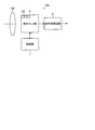
- FIG. 3 is a cross-sectional view showing a schematic configuration example of the image pickup apparatus according to the first embodiment. It is a block diagram which shows the schematic structural example of the image sensor for non-visible light which concerns on 1st Embodiment.
- FIG. 3 is a block diagram showing a schematic configuration example of an image sensor for visible light according to the first embodiment. It is a figure which shows an example of the scattering angle profile of the diffusion plate which concerns on 1st Embodiment. It is a figure for demonstrating another example of the diffuser plate which concerns on 1st Embodiment. It is a figure for demonstrating the reflected light at the time of using the diffuser plate shown in FIG. FIG.
- the diffuser plate is arranged sufficiently close to the light receiving surface of the image sensor, for example, so that the diffusion of light by the diffuser plate does not affect the image quality. That is, since the incident light heading for the image sensor becomes light (hereinafter referred to as “scattered light”) whose diameter expands according to the propagation distance by passing through the diffusion plate, the distance from the diffusion plate to the light receiving surface of the image sensor is long. Then, the image formed on the light-receiving surface is blurred and the image quality is degraded. Therefore, in the present embodiment, the diffusion plate is arranged sufficiently close to the light receiving surface of the image sensor so that the image formed on the light receiving surface of the image sensor is not blurred.
- the light-receiving surface of the image sensor may be a surface on which the light-incident surface of the light-receiving element forming the unit pixel described later is arranged.
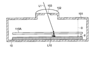
- the distance from the light receiving surface of the image sensor 10 to the upper surface of the inner wall of the housing 101 is D, and the diffusion plate 110 (for example, incident light is diffused from the light receiving surface of the image sensor 10).
- the distance from the positive direction to the plate 110 to the incident surface) is d.
- the upper surface of the image sensor 10 and the light receiving surface are shown as being in agreement, but they are not necessarily in agreement.
- the light receiving element 132 when a light receiving element 132 described later is formed at a predetermined depth from the upper surface of the image sensor 10, or when a microlens array or the like is provided on the upper surface of the image sensor 10, the light receiving element 132 receives light.
- the surface is located deeper than the upper surface of the image sensor 10.
- the light incident on the image sensor 10 may be reflected not only on the light receiving surface but also on the light incident surface of the image sensor 10 itself. In the following, for simplification of description, the light receiving surface and the incident surface will not be distinguished.
- the element array unit 3 includes, for example, a plurality of light receiving elements 132 arranged in a two-dimensional matrix in the row direction and the column direction. In FIG. 3, for simplification of description, some of the rows and columns in the pixel array unit 13 are omitted, but for example, tens to thousands of light receiving elements 132 are arranged in each row and each column. obtain.
- the lens 102 is arranged at a position where an image of the light L1 is formed on the light receiving surface on which the light receiving elements 132 are arranged.
- the pixel array unit 13 includes a plurality of unit pixels 131 arranged in a two-dimensional matrix in the row and column directions. In FIG. 4, some of rows and columns in the pixel array unit 13 are omitted for simplification of description, but for example, several tens to several thousands of unit pixels 131 are arranged in each row and each column. obtain.
- each unit pixel 131 is connected to the pixel drive circuit 12 via a pixel drive line LD for pixel selection, and is also connected to the signal processing circuit 15 via a vertical signal line VSL.
- the pixel drive line LD refers to all wirings that enter the unit pixel 131 from the pixel drive circuit 12.
- the pixel drive line LD may include a control line that propagates various pulse signals (for example, pixel reset pulse, transfer pulse, drain line control pulse, etc.) for driving the unit pixel 131.
- the signal processing circuit 15 includes an analog circuit such as an AD (Analog to Digital) conversion circuit that converts an analog pixel signal read from the unit pixel 131 into a digital pixel signal, and a digital value converted by the AD conversion circuit. It includes a logic circuit that executes digital processing such as CDS (correlated double sampling) processing based on pixel signals.
- the AD conversion circuit may be provided, for example, one-to-one for each unit pixel 131, or one-to-one for each pixel group configured by a plurality of unit pixels 131. Alternatively, each column in the pixel array section 13 may be provided in a one-to-one relationship.
- the reference voltage generator 17 supplies a reference voltage REF for converting the analog pixel signal read from each unit pixel 131 to a digital pixel signal via the vertical signal line VSL to the signal processing circuit 15.
- the pixel drive circuit 12 selects a row of the pixel array unit 13 and outputs a pulse required for driving the row to the pixel drive line LD. For example, a pulse is applied to a vertical decoder that defines a vertical read row (selects a row of the pixel array unit 13) and a pixel drive line LD for a unit pixel 131 on a read address (row direction) defined by the vertical decoder. And a vertical drive unit for driving the same.
- the vertical decoder selects not only the row from which the pixel signal is read but also the row for the electronic shutter.
- the horizontal transfer circuit 18 performs a shift operation (scanning) according to the column address signal input from the timing control circuit 11 to read a digital pixel signal from the AD conversion circuit of the readout column designated by the column address signal to the horizontal signal line HSL. Run.
- the image sensor 10B may be provided with a clock conversion unit that is an example of a high-speed clock generation unit and that generates a pulse having a clock frequency higher than the input clock frequency.
- the timing control circuit 11 may generate the internal clock based on an input lock (for example, a master clock) input from the outside or a high-speed clock generated by the clock conversion unit.
- the image sensor 10B for visible light is not limited to the CMOS (Complementary Metal Oxide Semiconductor) type image sensor described above, and various image sensors such as CCD (Charge Coupled Device) type can be applied. Is.
- CMOS Complementary Metal Oxide Semiconductor
- CCD Charge Coupled Device
- FIG. 8 is a diagram for explaining how light that has entered the imaging device according to the present embodiment enters the light-receiving surface of the image sensor.
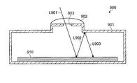
- FIG. 9 is a diagram for explaining secondary reflected light in the imaging device according to the present embodiment. It is to be noted that FIG. 9 shows a state in which the light L11 reflected by the image sensor 10 is reflected by the ceiling 101a of the housing 101 and is incident on the image sensor 10 again.
- the distance (for example, the shortest distance) d from the light receiving surface of the image sensor 10 to the diffusion plate 110 (for example, the surface on which the incident light is incident on the diffusion plate 110 in the positive direction) is sufficiently short, that is, the diffusion plate.
- the diffusion plate 110 When 110 is sufficiently close to the light receiving surface of the image sensor 10, it is possible to reduce blurring of an image formed on the light receiving surface and suppress deterioration of image quality.
- the diffuser plate 110 and the image sensor 10 are arranged close to each other such that the light L10 that is incident on the diffuser plate 110 and diffused near the center of each light-receiving element 132 does not enter the adjacent light-receiving element 132.
- the formula (3) shows a case where the light L1 is vertically incident on the diffusion plate 110.
- the shape and size of the spot formed on the light receiving surface of the image sensor 10 by the light L10 diffused by the diffusion plate 110 also depends on the incident angle ⁇ of the light L1 on the diffusion plate 110.
- the diffusion plate 110 has a spatially non-uniform profile in which the smaller the incident angle ⁇ , the stronger the diffusion around the spot.
- the diffusion plate 110 also has a function of changing the distance between the light receiving surface of the image sensor 10 and the diffusion plate 110 depending on the incident angle ⁇ . That is, the greater the incident angle ⁇ , the shorter the distance from the light receiving surface of the image sensor 10 to the diffusion plate 110.
- FIG. 11 is a schematic diagram for explaining artifacts due to secondary reflection in the present embodiment.
- the spread due to diffusion received by the diffusion plate 110 when the light L13 reflected by the ceiling 101a of the housing 101 is incident on the image sensor 10 again is ignored. This is because the light path length until the light L13 reflected by the image sensor 10 re-enters the image sensor 10 is shorter than the light path length until the light L13 reflected by the image sensor 10 re-enters the image sensor 10, This is because even if the influence is ignored, the result of the consideration is hardly influenced.
- the radius R can be made much larger than the radius r by setting the distance D sufficiently larger than the distance d. From this, the distance d from the light receiving surface of the image sensor 10 to the diffusion plate 110 is sufficiently short, that is, the diffusion plate 110 is sufficiently close to the light receiving surface of the image sensor 10 to form an image on the light receiving surface. It can be seen that it is possible to reduce the blur of the image and suppress the deterioration of the image quality.
- the diffusion plate 110 is arranged in proximity to the light receiving surface of the image sensor 10 housed in the housing 101. This makes it possible to sufficiently blur the image of the light L14 reflected by the image sensor 10 and reflected by the surrounding reflective member (for example, the ceiling 101a) and then incident on the image sensor 10 to a negligible extent. Therefore, it is possible to reduce the artifact due to the secondary reflection.
- the diffusion plate 110 is arranged sufficiently close to the light receiving surface of the image sensor 10. As a result, blurring of the image of the light L10 formed on the light receiving surface of the image sensor 10 is reduced, and thus it is possible to suppress deterioration of image quality.
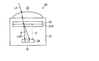
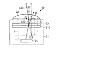
- the image sensor 20 includes, for example, a semiconductor substrate 21 such as a silicon substrate on which a filter 23, a diffusion unit 210, and a light receiving unit 24 are formed.
- a microlens 22 for each unit pixel is provided on the light incident surface of the semiconductor substrate 21.
- the microlens 22 condenses the incident light L2 on the light receiving unit 24, for example.
- the filter 23 has a wavelength selection function of transmitting light of a specific wavelength, for example.
- the diffusion unit 210 diffuses the incident light with a predetermined scattering angle profile and outputs the scattered light L20.
- the light receiving unit 24 images the incident light and generates an electric charge, similarly to the light receiving element 132 in the above-described embodiment.
- the diffusion unit 210 is arranged, for example, between the filter 23 and the light receiving unit 24.
- the diffusion unit 210 is arranged immediately below the filter 23.
- the distance d from the light incident surface of the light receiving unit 24 to the diffusion unit 210 is sufficiently short. That is, the diffusion plate 110 can be sufficiently close to the light receiving surface of the image sensor 10.
- the light L2 that has entered the microlens 22 then enters the diffusing section 210 via the filter 23 formed on the semiconductor substrate 21, and thus the scattering angle ⁇ of It is converted into scattered light L20. Then, the scattered light L20 propagates through the semiconductor substrate 21 and is incident on the light receiving portion 24 which is separated from the diffusion portion 210 by the distance d.
- the distance I is always a negative value, and the absolute value of the distance I is always smaller than the distance L. That is, the emission surface of the light L23, assuming that there is no diffusing unit 210, is located between the light receiving unit 24 and the diffusing unit 210 arranged at the distance I obtained from the equation (8).
- the scattering angle ⁇ 1 of the light L23 can be approximated by the following equation (9).
- the filter 23 and the diffusing unit 210 it is possible to use a layer in which the filter and the diffusing unit are integrated. Even in this case, the distance d from the light incident surface of the light receiving unit 24 to the diffusion unit 210 can be sufficiently shortened as in the above-described configuration, and thus an image is formed on the light receiving surface of the image sensor 20. It is possible to reduce blurring of an image and suppress deterioration of image quality.
- the diffusion plate 110 is arranged close to the light receiving surface of the image sensor 10. As a result, it is possible to reduce the blurring of the image formed on the light receiving surface and suppress the deterioration of image quality.
- the image sensor 10 is configured to have a sufficiently long length.
- the diameter of the light L23 can be sufficiently widened to reduce its intensity. Thereby, it is possible to reduce the artifacts due to the secondary reflection.
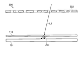
- the light L1 incident through the optical aperture of the coded aperture 302 is incident on the point P on the light receiving surface of the image sensor 10. Further, the light L92 reflected at the point P is reflected by the light-shielding portion of the coded aperture 302, and the reflected light L93 due to this reflection enters the point Q on the light receiving surface of the image sensor 10. Therefore, the spots of light formed on the light receiving surface of the image sensor 10 are the two points P and Q.
Landscapes
- Physics & Mathematics (AREA)
- General Physics & Mathematics (AREA)
- Spectroscopy & Molecular Physics (AREA)
- Multimedia (AREA)
- Signal Processing (AREA)
- Engineering & Computer Science (AREA)
- Health & Medical Sciences (AREA)
- Toxicology (AREA)
- Optics & Photonics (AREA)
- Solid State Image Pick-Up Elements (AREA)
- Transforming Light Signals Into Electric Signals (AREA)
- Photometry And Measurement Of Optical Pulse Characteristics (AREA)
- Light Receiving Elements (AREA)
Abstract
Le but de la présente invention est de réduire les artefacts provoqués par une réflexion secondaire. Un dispositif d'imagerie appartenant à un mode de réalisation comporte : une partie de diffusion (110) qui convertit une lumière incidente en lumière diffusée, dont le diamètre augmente en fonction de la distance de propagation de celle-ci, et émet la lumière diffusée; et une partie de réception de lumière (132) pour convertir la lumière diffusée provenant de la partie de diffusion en un signal électrique.
Priority Applications (4)
| Application Number | Priority Date | Filing Date | Title |
|---|---|---|---|
| EP19873204.2A EP3869794A4 (fr) | 2018-10-19 | 2019-08-26 | Dispositif d'imagerie et dispositif d'imagerie à semi-conducteurs |
| US17/284,600 US11546530B2 (en) | 2018-10-19 | 2019-08-26 | Imaging device and solid-state imaging device |
| JP2020552560A JPWO2020079960A1 (ja) | 2018-10-19 | 2019-08-26 | 撮像装置及び固体撮像装置 |
| CN201980067143.5A CN113170062A (zh) | 2018-10-19 | 2019-08-26 | 成像装置和固态成像装置 |
Applications Claiming Priority (2)
| Application Number | Priority Date | Filing Date | Title |
|---|---|---|---|
| JP2018-197319 | 2018-10-19 | ||
| JP2018197319 | 2018-10-19 |
Publications (1)
| Publication Number | Publication Date |
|---|---|
| WO2020079960A1 true WO2020079960A1 (fr) | 2020-04-23 |
Family
ID=70284567
Family Applications (1)
| Application Number | Title | Priority Date | Filing Date |
|---|---|---|---|
| PCT/JP2019/033232 Ceased WO2020079960A1 (fr) | 2018-10-19 | 2019-08-26 | Dispositif d'imagerie et dispositif d'imagerie à semi-conducteurs |
Country Status (5)
| Country | Link |
|---|---|
| US (1) | US11546530B2 (fr) |
| EP (1) | EP3869794A4 (fr) |
| JP (1) | JPWO2020079960A1 (fr) |
| CN (1) | CN113170062A (fr) |
| WO (1) | WO2020079960A1 (fr) |
Cited By (1)
| Publication number | Priority date | Publication date | Assignee | Title |
|---|---|---|---|---|
| WO2022202054A1 (fr) * | 2021-03-26 | 2022-09-29 | ソニーグループ株式会社 | Analyseur d'échantillons biologiques et cytomètre de flux |
Families Citing this family (2)
| Publication number | Priority date | Publication date | Assignee | Title |
|---|---|---|---|---|
| WO2020079960A1 (fr) * | 2018-10-19 | 2020-04-23 | ソニー株式会社 | Dispositif d'imagerie et dispositif d'imagerie à semi-conducteurs |
| DE102019123404B4 (de) * | 2019-09-02 | 2024-02-15 | Bayerische Motoren Werke Aktiengesellschaft | Sensorvorrichtung und Fahrassistenzsystem |
Citations (8)
| Publication number | Priority date | Publication date | Assignee | Title |
|---|---|---|---|---|
| JP2004266250A (ja) * | 2003-02-12 | 2004-09-24 | Inter Action Corp | 固体撮像素子の試験装置、中継装置および光学モジュール |
| JP2005331371A (ja) * | 2004-05-20 | 2005-12-02 | Nikon Corp | 照明補助装置及びこの照明補助装置を用いた検査装置 |
| US20130334423A1 (en) | 2012-06-19 | 2013-12-19 | General Electric Company | Non-Dispersive Infrared Sensor with a Reflective Diffuser |
| US20140284748A1 (en) | 2011-01-26 | 2014-09-25 | Maxim Integrated Products, Inc. | Light sensor having transparent substrate and diffuser formed therein |
| WO2016091757A1 (fr) | 2014-12-08 | 2016-06-16 | Ams Ag | Capteur optique intégré et procédé de fabrication d'un capteur optique intégré |
| JP2016528496A (ja) * | 2013-08-02 | 2016-09-15 | ベリフード, リミテッドVerifood, Ltd. | 分光器システムおよび方法、分光分析デバイスおよび方法 |
| US9645008B2 (en) | 2014-08-25 | 2017-05-09 | Apple Inc. | Light sensor windows for electronic devices |
| US9891098B2 (en) | 2010-12-30 | 2018-02-13 | Apple Inc. | Diffuser and filter structures for light sensors |
Family Cites Families (8)
| Publication number | Priority date | Publication date | Assignee | Title |
|---|---|---|---|---|
| US20060214673A1 (en) | 2003-11-28 | 2006-09-28 | Shingo Tamai | Intrument for testing solid-state imaging device |
| US7738026B2 (en) | 2005-05-02 | 2010-06-15 | Andrew G. Cartlidge | Increasing fill-factor on pixelated sensors |
| JP2007047757A (ja) * | 2005-07-13 | 2007-02-22 | Sony Corp | 透過型スクリーンの製造方法、その製造装置および透過型スクリーン |
| US7423821B2 (en) | 2006-03-24 | 2008-09-09 | Gentex Corporation | Vision system |
| US9405124B2 (en) * | 2013-04-09 | 2016-08-02 | Massachusetts Institute Of Technology | Methods and apparatus for light field projection |
| CN106170052B (zh) * | 2015-05-22 | 2020-11-06 | 微软技术许可有限责任公司 | 双传感器超光谱运动成像系统 |
| US10783652B2 (en) * | 2016-05-06 | 2020-09-22 | Arizona Board Of Regents On Behalf Of The University Of Arizona | Plenoptic imaging apparatus, method, and applications |
| WO2020079960A1 (fr) * | 2018-10-19 | 2020-04-23 | ソニー株式会社 | Dispositif d'imagerie et dispositif d'imagerie à semi-conducteurs |
-
2019
- 2019-08-26 WO PCT/JP2019/033232 patent/WO2020079960A1/fr not_active Ceased
- 2019-08-26 CN CN201980067143.5A patent/CN113170062A/zh not_active Withdrawn
- 2019-08-26 JP JP2020552560A patent/JPWO2020079960A1/ja not_active Abandoned
- 2019-08-26 US US17/284,600 patent/US11546530B2/en active Active
- 2019-08-26 EP EP19873204.2A patent/EP3869794A4/fr not_active Withdrawn
Patent Citations (8)
| Publication number | Priority date | Publication date | Assignee | Title |
|---|---|---|---|---|
| JP2004266250A (ja) * | 2003-02-12 | 2004-09-24 | Inter Action Corp | 固体撮像素子の試験装置、中継装置および光学モジュール |
| JP2005331371A (ja) * | 2004-05-20 | 2005-12-02 | Nikon Corp | 照明補助装置及びこの照明補助装置を用いた検査装置 |
| US9891098B2 (en) | 2010-12-30 | 2018-02-13 | Apple Inc. | Diffuser and filter structures for light sensors |
| US20140284748A1 (en) | 2011-01-26 | 2014-09-25 | Maxim Integrated Products, Inc. | Light sensor having transparent substrate and diffuser formed therein |
| US20130334423A1 (en) | 2012-06-19 | 2013-12-19 | General Electric Company | Non-Dispersive Infrared Sensor with a Reflective Diffuser |
| JP2016528496A (ja) * | 2013-08-02 | 2016-09-15 | ベリフード, リミテッドVerifood, Ltd. | 分光器システムおよび方法、分光分析デバイスおよび方法 |
| US9645008B2 (en) | 2014-08-25 | 2017-05-09 | Apple Inc. | Light sensor windows for electronic devices |
| WO2016091757A1 (fr) | 2014-12-08 | 2016-06-16 | Ams Ag | Capteur optique intégré et procédé de fabrication d'un capteur optique intégré |
Non-Patent Citations (1)
| Title |
|---|
| See also references of EP3869794A4 |
Cited By (3)
| Publication number | Priority date | Publication date | Assignee | Title |
|---|---|---|---|---|
| WO2022202054A1 (fr) * | 2021-03-26 | 2022-09-29 | ソニーグループ株式会社 | Analyseur d'échantillons biologiques et cytomètre de flux |
| JPWO2022202054A1 (fr) * | 2021-03-26 | 2022-09-29 | ||
| US12571731B2 (en) | 2021-03-26 | 2026-03-10 | Sony Group Corporation | Biological sample analyzer and flow cytometer |
Also Published As
| Publication number | Publication date |
|---|---|
| EP3869794A4 (fr) | 2022-04-20 |
| EP3869794A1 (fr) | 2021-08-25 |
| US11546530B2 (en) | 2023-01-03 |
| JPWO2020079960A1 (ja) | 2021-09-30 |
| US20210258517A1 (en) | 2021-08-19 |
| CN113170062A (zh) | 2021-07-23 |
Similar Documents
| Publication | Publication Date | Title |
|---|---|---|
| US11575843B2 (en) | Image sensor modules including primary high-resolution imagers and secondary imagers | |
| KR102377023B1 (ko) | 다중 f-수 렌즈를 위한 방법 및 시스템 | |
| CN102538955B (zh) | 辐射传感器 | |
| JP6172982B2 (ja) | 撮像装置及びカメラシステム | |
| US10728506B2 (en) | Optical filter, solid state imaging device, and electronic apparatus | |
| CN102623464B (zh) | 固态图像传感器和照相机 | |
| JP2019529958A (ja) | 物体までの距離を決定するためのシステム及び方法 | |
| US10644050B2 (en) | Image sensor having micro lenses arranged in different periods | |
| WO2020079960A1 (fr) | Dispositif d'imagerie et dispositif d'imagerie à semi-conducteurs | |
| US11658195B2 (en) | Image sensor including microlenses having different shapes | |
| WO2022168907A1 (fr) | Dispositif d'imagerie à semi-conducteur, procédé de fabrication de dispositif d'imagerie à semi-conducteur et appareil électronique | |
| US8319167B2 (en) | Solid state imaging device and electronic apparatus | |
| JP2014239290A (ja) | 焦点検出装置、電子機器、製造装置、製造方法 | |
| JP2014165778A (ja) | 固体撮像素子、撮像装置及び焦点検出装置 | |
| US20050190284A1 (en) | Imaging apparatus and arranging method for the same | |
| JP2020017791A (ja) | 固体撮像装置 | |
| JP4809859B2 (ja) | 画像読取装置 | |
| US12484326B2 (en) | Imaging array with directional response | |
| JP2009086144A (ja) | 撮像装置及びそれを有する撮像機器 | |
| US12299946B2 (en) | Highly efficient active illumination imaging systems and methods | |
| CN116670535A (zh) | 距离测量系统 | |
| CN114402226A (zh) | 光学传感器 | |
| JP2006324810A (ja) | 光学モジュール | |
| CN109314121B (zh) | 成像装置和电子设备 | |
| CN119335502A (zh) | 光探测芯片、发光芯片及激光雷达 |
Legal Events
| Date | Code | Title | Description |
|---|---|---|---|
| 121 | Ep: the epo has been informed by wipo that ep was designated in this application |
Ref document number: 19873204 Country of ref document: EP Kind code of ref document: A1 |
|
| ENP | Entry into the national phase |
Ref document number: 2020552560 Country of ref document: JP Kind code of ref document: A |
|
| NENP | Non-entry into the national phase |
Ref country code: DE |
|
| ENP | Entry into the national phase |
Ref document number: 2019873204 Country of ref document: EP Effective date: 20210519 |