EP0834916A2 - Verfahren zur Herstellung einer Halbleiterstruktur mit Gebieten, die aus Materialen mit niedriger dielektrischer Konstante hergestellt sind - Google Patents
Verfahren zur Herstellung einer Halbleiterstruktur mit Gebieten, die aus Materialen mit niedriger dielektrischer Konstante hergestellt sind Download PDFInfo
- Publication number
- EP0834916A2 EP0834916A2 EP97116851A EP97116851A EP0834916A2 EP 0834916 A2 EP0834916 A2 EP 0834916A2 EP 97116851 A EP97116851 A EP 97116851A EP 97116851 A EP97116851 A EP 97116851A EP 0834916 A2 EP0834916 A2 EP 0834916A2
- Authority
- EP
- European Patent Office
- Prior art keywords
- dielectric layer
- forming
- conductive
- layer
- dielectric
- Prior art date
- Legal status (The legal status is an assumption and is not a legal conclusion. Google has not performed a legal analysis and makes no representation as to the accuracy of the status listed.)
- Withdrawn
Links
Images


Classifications
-
- H—ELECTRICITY
- H10—SEMICONDUCTOR DEVICES; ELECTRIC SOLID-STATE DEVICES NOT OTHERWISE PROVIDED FOR
- H10W—GENERIC PACKAGES, INTERCONNECTIONS, CONNECTORS OR OTHER CONSTRUCTIONAL DETAILS OF DEVICES COVERED BY CLASS H10
- H10W20/00—Interconnections in chips, wafers or substrates
- H10W20/01—Manufacture or treatment
- H10W20/031—Manufacture or treatment of conductive parts of the interconnections
- H10W20/063—Manufacture or treatment of conductive parts of the interconnections by forming conductive members before forming protective insulating material
-
- H—ELECTRICITY
- H10—SEMICONDUCTOR DEVICES; ELECTRIC SOLID-STATE DEVICES NOT OTHERWISE PROVIDED FOR
- H10W—GENERIC PACKAGES, INTERCONNECTIONS, CONNECTORS OR OTHER CONSTRUCTIONAL DETAILS OF DEVICES COVERED BY CLASS H10
- H10W20/00—Interconnections in chips, wafers or substrates
- H10W20/01—Manufacture or treatment
-
- H—ELECTRICITY
- H10—SEMICONDUCTOR DEVICES; ELECTRIC SOLID-STATE DEVICES NOT OTHERWISE PROVIDED FOR
- H10W—GENERIC PACKAGES, INTERCONNECTIONS, CONNECTORS OR OTHER CONSTRUCTIONAL DETAILS OF DEVICES COVERED BY CLASS H10
- H10W20/00—Interconnections in chips, wafers or substrates
- H10W20/01—Manufacture or treatment
- H10W20/071—Manufacture or treatment of dielectric parts thereof
- H10W20/072—Manufacture or treatment of dielectric parts thereof of dielectric parts comprising air gaps
-
- H—ELECTRICITY
- H10—SEMICONDUCTOR DEVICES; ELECTRIC SOLID-STATE DEVICES NOT OTHERWISE PROVIDED FOR
- H10W—GENERIC PACKAGES, INTERCONNECTIONS, CONNECTORS OR OTHER CONSTRUCTIONAL DETAILS OF DEVICES COVERED BY CLASS H10
- H10W20/00—Interconnections in chips, wafers or substrates
- H10W20/01—Manufacture or treatment
- H10W20/071—Manufacture or treatment of dielectric parts thereof
- H10W20/074—Manufacture or treatment of dielectric parts thereof of dielectric parts comprising thin functional dielectric layers, e.g. dielectric etch-stop, barrier, capping or liner layers
- H10W20/077—Manufacture or treatment of dielectric parts thereof of dielectric parts comprising thin functional dielectric layers, e.g. dielectric etch-stop, barrier, capping or liner layers on sidewalls or on top surfaces of conductors
-
- H—ELECTRICITY
- H10—SEMICONDUCTOR DEVICES; ELECTRIC SOLID-STATE DEVICES NOT OTHERWISE PROVIDED FOR
- H10W—GENERIC PACKAGES, INTERCONNECTIONS, CONNECTORS OR OTHER CONSTRUCTIONAL DETAILS OF DEVICES COVERED BY CLASS H10
- H10W20/00—Interconnections in chips, wafers or substrates
- H10W20/01—Manufacture or treatment
- H10W20/071—Manufacture or treatment of dielectric parts thereof
- H10W20/081—Manufacture or treatment of dielectric parts thereof by forming openings in the dielectric parts
- H10W20/084—Manufacture or treatment of dielectric parts thereof by forming openings in the dielectric parts for dual-damascene structures
-
- H—ELECTRICITY
- H10—SEMICONDUCTOR DEVICES; ELECTRIC SOLID-STATE DEVICES NOT OTHERWISE PROVIDED FOR
- H10W—GENERIC PACKAGES, INTERCONNECTIONS, CONNECTORS OR OTHER CONSTRUCTIONAL DETAILS OF DEVICES COVERED BY CLASS H10
- H10W20/00—Interconnections in chips, wafers or substrates
- H10W20/01—Manufacture or treatment
- H10W20/071—Manufacture or treatment of dielectric parts thereof
- H10W20/081—Manufacture or treatment of dielectric parts thereof by forming openings in the dielectric parts
- H10W20/084—Manufacture or treatment of dielectric parts thereof by forming openings in the dielectric parts for dual-damascene structures
- H10W20/085—Manufacture or treatment of dielectric parts thereof by forming openings in the dielectric parts for dual-damascene structures involving intermediate temporary filling with material
-
- H—ELECTRICITY
- H10—SEMICONDUCTOR DEVICES; ELECTRIC SOLID-STATE DEVICES NOT OTHERWISE PROVIDED FOR
- H10W—GENERIC PACKAGES, INTERCONNECTIONS, CONNECTORS OR OTHER CONSTRUCTIONAL DETAILS OF DEVICES COVERED BY CLASS H10
- H10W20/00—Interconnections in chips, wafers or substrates
- H10W20/01—Manufacture or treatment
- H10W20/071—Manufacture or treatment of dielectric parts thereof
- H10W20/093—Manufacture or treatment of dielectric parts thereof by modifying materials of the dielectric parts
- H10W20/097—Manufacture or treatment of dielectric parts thereof by modifying materials of the dielectric parts by thermally treating
-
- H—ELECTRICITY
- H10—SEMICONDUCTOR DEVICES; ELECTRIC SOLID-STATE DEVICES NOT OTHERWISE PROVIDED FOR
- H10W—GENERIC PACKAGES, INTERCONNECTIONS, CONNECTORS OR OTHER CONSTRUCTIONAL DETAILS OF DEVICES COVERED BY CLASS H10
- H10W20/00—Interconnections in chips, wafers or substrates
- H10W20/40—Interconnections external to wafers or substrates, e.g. back-end-of-line [BEOL] metallisations or vias connecting to gate electrodes
- H10W20/45—Interconnections external to wafers or substrates, e.g. back-end-of-line [BEOL] metallisations or vias connecting to gate electrodes characterised by their insulating parts
- H10W20/46—Interconnections external to wafers or substrates, e.g. back-end-of-line [BEOL] metallisations or vias connecting to gate electrodes characterised by their insulating parts comprising air gaps
-
- H—ELECTRICITY
- H10—SEMICONDUCTOR DEVICES; ELECTRIC SOLID-STATE DEVICES NOT OTHERWISE PROVIDED FOR
- H10W—GENERIC PACKAGES, INTERCONNECTIONS, CONNECTORS OR OTHER CONSTRUCTIONAL DETAILS OF DEVICES COVERED BY CLASS H10
- H10W20/00—Interconnections in chips, wafers or substrates
- H10W20/40—Interconnections external to wafers or substrates, e.g. back-end-of-line [BEOL] metallisations or vias connecting to gate electrodes
- H10W20/45—Interconnections external to wafers or substrates, e.g. back-end-of-line [BEOL] metallisations or vias connecting to gate electrodes characterised by their insulating parts
- H10W20/48—Insulating materials thereof
-
- H—ELECTRICITY
- H10—SEMICONDUCTOR DEVICES; ELECTRIC SOLID-STATE DEVICES NOT OTHERWISE PROVIDED FOR
- H10W—GENERIC PACKAGES, INTERCONNECTIONS, CONNECTORS OR OTHER CONSTRUCTIONAL DETAILS OF DEVICES COVERED BY CLASS H10
- H10W20/00—Interconnections in chips, wafers or substrates
- H10W20/40—Interconnections external to wafers or substrates, e.g. back-end-of-line [BEOL] metallisations or vias connecting to gate electrodes
- H10W20/495—Capacitive arrangements or effects of, or between wiring layers
-
- H—ELECTRICITY
- H10—SEMICONDUCTOR DEVICES; ELECTRIC SOLID-STATE DEVICES NOT OTHERWISE PROVIDED FOR
- H10W—GENERIC PACKAGES, INTERCONNECTIONS, CONNECTORS OR OTHER CONSTRUCTIONAL DETAILS OF DEVICES COVERED BY CLASS H10
- H10W20/00—Interconnections in chips, wafers or substrates
- H10W20/01—Manufacture or treatment
- H10W20/071—Manufacture or treatment of dielectric parts thereof
-
- H—ELECTRICITY
- H10—SEMICONDUCTOR DEVICES; ELECTRIC SOLID-STATE DEVICES NOT OTHERWISE PROVIDED FOR
- H10W—GENERIC PACKAGES, INTERCONNECTIONS, CONNECTORS OR OTHER CONSTRUCTIONAL DETAILS OF DEVICES COVERED BY CLASS H10
- H10W20/00—Interconnections in chips, wafers or substrates
- H10W20/01—Manufacture or treatment
- H10W20/071—Manufacture or treatment of dielectric parts thereof
- H10W20/081—Manufacture or treatment of dielectric parts thereof by forming openings in the dielectric parts
- H10W20/084—Manufacture or treatment of dielectric parts thereof by forming openings in the dielectric parts for dual-damascene structures
- H10W20/0886—Manufacture or treatment of dielectric parts thereof by forming openings in the dielectric parts for dual-damascene structures involving forming a via in a via-level dielectric prior to deposition of a trench-level dielectric
-
- H—ELECTRICITY
- H10—SEMICONDUCTOR DEVICES; ELECTRIC SOLID-STATE DEVICES NOT OTHERWISE PROVIDED FOR
- H10W—GENERIC PACKAGES, INTERCONNECTIONS, CONNECTORS OR OTHER CONSTRUCTIONAL DETAILS OF DEVICES COVERED BY CLASS H10
- H10W20/00—Interconnections in chips, wafers or substrates
- H10W20/01—Manufacture or treatment
- H10W20/071—Manufacture or treatment of dielectric parts thereof
- H10W20/081—Manufacture or treatment of dielectric parts thereof by forming openings in the dielectric parts
- H10W20/084—Manufacture or treatment of dielectric parts thereof by forming openings in the dielectric parts for dual-damascene structures
- H10W20/0888—Manufacture or treatment of dielectric parts thereof by forming openings in the dielectric parts for dual-damascene structures wherein via-level dielectrics are compositionally different than trench-level dielectrics
Definitions
- the present invention relates generally to semiconductor manufacturing, and more particularly, in forming low dielectric constant regions between metallic members to reduce capacitive coupling and cross-talk.
- Modern integrated circuits contain thousands of semiconducting devices on a single chip and as the device density of a given chip increases more layers of metallization are required to interconnect the devices. Moreover, within a given metal layer, the horizontal distance separating metallization lines must be reduced in order to minimize the chip size as integrated circuit device density increases. At the same time, metallization resistance and capacitance must be minimized in order to meet the chip's speed and performance requirements.
- the inter-level dielectrics used to isolate metallization lines within a same level and metallization lines in two different levels have been performed using materials with high dielectric constants.
- borophosphosilicate glass borophosphosilicate glass (BPSG), phosphosilicate glass (PSG), and plasma and chemical vapor deposited tetraethylorthosilicate based (TEOS) oxides have been used as dielectric layers in these multi-metallization structures.
- BPSG borophosphosilicate glass
- PSG phosphosilicate glass
- TEOS plasma and chemical vapor deposited tetraethylorthosilicate based oxides
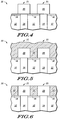
- FIGs. 1-6 illustrate, in cross-sectional diagrams, process steps for making an interconnect structure in accordance with one embodiment of the invention.
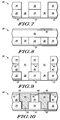
- FIGs. 7-10 illustrate, in cross-sectional diagrams, process steps for making an interconnect structure in accordance with an alternative of embodiment of the invention.
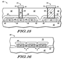
- FIGs. 11-15 illustrate, in cross-sectional diagrams, process steps for making an interconnect structure in accordance with yet another alternative embodiment of the invention.
- FIG. 16 illustrates, in a cross-sectional diagram, an interconnect structure wherein air gaps are formed by a material deposited via a non-conformal deposition process in accordance with one embodiment of the invention.
- an interconnect structure is formed using a first dielectric layer with a high dielectric constant and a second dielectric layer with a low dielectric constant.
- the dielectric layer having a low dielectric constant is formed predominantly between conductive interconnects and not substantially over the conductive interconnects.
- the low-K dielectric material is formed in this manner after a sacrificial higher-K dielectric layer between the interconnects has been removed to provide areas between conductive members which can be filled low-K dielectric material whereby low-K dielectric material over the conductive members is reduced or eliminated. This select placement of low-K material to between conductive regions instead of overlying or underlying conductive member improves thermal dissipation and mechanical strength while preserving the advantage of improved isolation associated with the low-K material.
- an interconnect structure having reduced cross-talk or RC time delays is formed by etching a first dielectric layer to form a contact opening.
- a second dielectric layer is then deposited wherein the second dielectric layer has a low dielectric constant.
- the second dielectric layer is deposited such that the contact opening in the first dielectric layer is sealed to form an air region (e.g., the second dielectric can be a low-K spin-on-resin with a stiff polymer backbone).
- a portion of the second dielectric layer is then removed to expose the contact opening previously sealed by the second dielectric layer.
- a dual in-laid metal interconnect is then formed within the contact opening whereby the low-K second dielectric is positioned between conductive regions where isolation benefits are achieved while thermal and mechanical properties are improved.
- void/air regions are formed between adjacent conductive metal interconnect lines by spinning on a polymeric resin having a stiff polymer backbone.
- This stiff backbone material forms air regions between closely spaced metal conductive members within the same conductive interconnect layer.
- a non-conformal dielectric layer is formed overlying adjacent conductive interconnect lines such that a void/air region is formed between closely-spaced conductive interconnect lines within the same conductive interconnect level.
- a second dielectric layer is then formed overlying the non-conformal dielectric layer and planarized to form a completed inter-level dielectric.
- the second dielectric layer and the non-conformal conductive layer are then patterned to form a contact or via opening which is then filled with conductive material to form a conductive interconnect.
- the void region between the two adjacent conductive interconnect lines reduces cross-talk/capacitance between the two conductive interconnect lines so that circuit speed is improved and logical cross-talk errors are avoided.
- FIGs. 1-16 The embodiments of the present invention can be further understood with reference to FIGs. 1-16.
- FIGs. 1-6 illustrate, in cross-sectional form, process steps for making an interconnect structure in accordance with a first embodiment of the invention.
- Shown in FIG. 1 is a portion 10 of an integrated circuit structure comprising a first dielectric layer 12, an etch stop layer 16, and a second dielectric layer 18.
- first dielectric layer 12, etch stop layer 16, and second dielectric layer 18 are patterned using conventional lithographic and etching techniques.
- first dielectric layer 12, etch stop layer 16, and second dielectric layer 18 are simultaneously patterned and etched using a plasma etch chemistry comprising a fluorinated etch species.
- the layers 12, 16, and 18 may be patterned in a plasma environment which is generated using etch gases such as CHF 3 , CF 4 , C 2 F 6 and/or the like. It is important to note that this etch process defines a contact opening 14 within first dielectric layer 12 which allows a metallic conductive layer to be subsequently deposited within the contact opening of FIG. 1 to form a conductive contact portion 14. This subsequently deposited conductive layer is used to make electrical contact/interconnection to an underlying conductive region such as another metal layer or a doped semiconductive region within polysilicon layer or the semiconductor substrate.
- etch gases such as CHF 3 , CF 4 , C 2 F 6 and/or the like.
- the doped region may be a bipolar electrode, a well contact, a source/drain, a thin film transistor (TFT) node or a like doped polysilicon or substrate portion.
- Polysilicon may be replaced with amorphous silicon, epitaxially grown silicon, or refractory silicided silicon-containing layers.
- first dielectric layer 12 and second dielectric layer 18 are formed using the same material.
- first dielectric layer 12 and second dielectric layer 18 may be a layer of borophosphosilicate glass (BPSG), layers of plasma tetraethylorthosilicate (TEOS), phosphosilicate glass (PSG) layers, silicon dioxide, nitride layers, fluorinated oxide layers, or like dielectric materials.
- the dielectric layer 18 may be made of a different material from layer 12.
- First dielectric layer 12, second dielectric layer 18 are formed using conventional plasma deposition processes, low pressure chemical vapor position (LPCVD) processes, or the like.
- etch stop layer 16 is a layer of plasma enhanced silicon nitride when the layers 12 and 18 are oxide.
- etch stop layer 16 which can also function as an anti-reflective coating (ARC) used in lithographic processing, may be a layer of silicon rich silicon nitride, aluminum nitride, or any dielectric layer which can be used as an etch-back stopping layer or a chemical mechanical polishing (CMP) stop layer.
- silicon oxide nitride (SiON) or silicon rich SiON may be used as an etch stop or anti-reflective coating (ARC) layer herein.
- FIG. 2 another photoresist and etch process is used to form interconnect trenches within layer 18.
- the openings through layer 12 in FIG. 1 are contact openings to underlying material whereas the opening formed through layer 18 in FIG. 2 is an interconnect trench.
- the second dielectric layer 18 is etched selective to etch stop layer 16 using an etch chemistry environment. This etch process defines an interconnect region 20 within second dielectric layer 18. It is important to note that dual in-laid metal processing can be performed in other similar ways than that illustrated in FIGs. 1-2.
- FIGs. 1-2 are intended to be representative of any method for forming dual in-laid structures having contact areas and interconnect trenches.
- a conductive layer of material is then deposited within contact portion 14 and interconnect portion 20.
- This conductive layer of material is subsequently planarized by CMP and/or etch processing to form conductive interconnects 21.
- conductive interconnects 21 are formed by first depositing a thin barrier layer within contact portion 14 and interconnect portion 20 followed by a thicker conductive layer which more completely fills conductive portion 14 and interconnect portion 20. It should be appreciated that interconnect 21 may be formed using conventional chemical mechanical polishing (CMP) techniques, resist etch back (REB) techniques, and/or timed plasma etch processing.
- CMP chemical mechanical polishing
- REB resist etch back
- any layer or composite layer comprising titanium nitride, titanium tungsten, titanium, tantalum, tantalum nitride, tantalum silicon nitride, titanium silicon nitride, tungsten nitride or other like material may be used as barrier layers for the portions 14 and 20.
- barrier layers for the portions 14 and 20.
- copper, gold, silver, tungsten, aluminum, any composite thereof, or the like may be used as the thicker fill materials to form interconnect 21 over the barrier layer(s).
- conductive interconnect 21 may be formed using conventional chemical vapor deposition (CVD) techniques, electrode plating techniques, sputtering techniques, and/or selective deposition techniques.
- the remaining portions of second dielectric layer 18 are selectively removed to expose portions of etch stop layer 16. It should be appreciated that the remaining portions of dielectric layer 18 may be removed using conventional plasma and/or wet etching techniques. In one embodiment the remaining portions of dielectric layer 18 are removed using buffered HF solution. Alternatively, the remaining portions of dielectric layer 18 may be removed using the same etch process used to define interconnects 21.
- a third dielectric layer 22 having a low dielectric constant e is then formed over conductive interconnects 21.
- Adequate low-K dielectrics for use herein are such that e ⁇ 3.5. Even more reduction in cross-talk and capacitive coupling will result when a low-K dielectric having e ⁇ 3.0 is utilized.
- materials with e ⁇ 2.7 are optimal as inter-level dielectrics.
- Third dielectric layer 22 maybe formed using conventional spin-on techniques or chemical vapor deposition techniques.
- HSQ hydrogen silsesquioxane
- BCB benzocyclobutene
- PAE polyarylether
- Layer 22 may be an organic spin-on dielectric or organic dielectric layer formed by a CVD technique.
- dielectric 22 is then planarized to expose a top portion of conductive interconnects 21.
- the portion of interconnect 21 which is exposed is a top portion of the conductive interconnect portion 20 as illustrated in FIG. 6.
- dielectric layer 22 is planarized using conventional plasma etching techniques and/or chemical mechanical polishing. As shown in FIG. 6, this planarization results in a formation of an interconnect structure having a low dielectric constant dielectric layer 22 (e ⁇ 3.5) overlying another dielectric layer 12 and 16 having a higher dielectric constant (e > 3.5).
- layer 22 and/or top portions of the conductive interconnects of FIG. 6 may be covered by an optional anti-reflective coating (ARC) layer.
- ARC anti-reflective coating
- dielectric layer 22 which has a low dielectric constant improves circuit performance because capacitance between adjacent interconnect lines is reduced by lower-K films. Due to the fact that layer 22 does not cover the entire surface of the wafer (e.g. top portions of 20 are not covered by layer 22 in FIG. 6), mechanical stability is improved and thermal properties are increased for the integrated circuit. If copper is used as a conductive interconnect in FIG. 6, then a capping/barrier layer may be needed on top of the structure of FIG. 6 to isolate the copper from overlying materials.
- FIG. 7-10 illustrate, in cross-sectional form, process steps for making an interconnect structure in accordance with an alternative embodiment of the invention.
- Shown in FIG. 7 is a portion 30 of an integrated circuit structure comprising an etch stop layer 32, a first dielectric layer 34, and a photoresist layer 36.
- etch stop layer 32 and first dielectric layer 34 are etched to form a contact portion 38 within first dielectric layer 34 and to expose an underlying conductive region (not illustrated in FIG. 7) such as a metal interconnect, polysilicon, or doped silicon region.
- Layer 32 is formed using conventional plasma or chemical vapor deposition techniques and may be a layer of silicon nitride, silicon rich-silicon nitride or aluminum nitride and functions as an etch stop layer (ESL) and/or an anti-reflective coating (ARC) layer.
- First dielectric layer 34 is also formed using conventional chemical vapor deposition (CVD) techniques such as plasma deposition, low pressure chemical vapor deposition (LPCVD) and the like and may be a layer of BPSG, PSG, TEOS, fluorinated oxide, or like dielectric materials or composite layers.
- CVD chemical vapor deposition
- dielectric layer 40 having a low dielectric constant is formed over dielectric layer 34 such that contact portion 38 is capped or bridged by dielectric layer 40 and left unfilled (i.e., an air gap 38 is formed in FIG. 8 from the contact portion 38 of FIG. 7).
- An anti-reflective coating (ARC) layer 42 which also serves as a hard mask is then deposited over dielectric layer 40.
- dielectric layer 40 has a dielectric constant e of 3.0 or less, but can be any material less than e a 3.5 to confer electrical isolation benefits between adjacent conductive members.
- the polyimide may be formed from either a poly(amic) acid solution or a fully imidized polyimide in FIG. 8.
- the spin-on material used in FIG. 8 to make the layer 40 can be any material which has a substantially stiff polymer backbone so that the air regions 38 are at least partially formed in FIG. 8.
- an anneal step of the layer 40 should be performed in a thermal ramp manner.
- the ramp should start at less than 100°C and arrive, after a selected temperature ramp time period, at roughly 100°C to 300°C for solvent-removal annealing of the layer 40.
- a slower ramp thermal process will be more likely to avoid any blistering of the air gap 38 than a fast exposure to high temperatures.
- a sub-atmospheric spin-on process can be used to create air gaps 38 with reduced pressure or fewer trapped molecules/atoms. This sub-atmospheric process can reduce blistering effects by eliminating a high density of atoms within the gap 38.
- dielectric layer 40 is patterned using a plasma comprising oxygen, and photoresist mask 44 used to define the opening within dielectric layer 40 is removed at the same time that dielectric layer 40 is etched. Therefore, in this embodiment the etch process used to pattern dielectric layer 40 also simultaneously removes some or all of the photoresist mask 44 used to define the opening within dielectric layer 40.
- a barrier layer 49 and a conductive film material are then formed within contact opening 38 and interconnect region 41. A portion of the barrier layer 49 and the conductive film material are then selectively removed to form conductive interconnects 48 of FIG. 10.
- conductive interconnects 48 are formed using conventional plasma etching techniques.
- connective interconnects 48 may be formed using conventional chemical mechanical polishing (CMP) techniques.
- An etch stop layer 46 or anti-reflective coating (ARC) layer 46 is then formed overlying dielectric 40 and conductive interconnects 48. It should be appreciated that the process steps illustrated in FIGs.
- FIG. 10 may then be repeated in order to form an additional set of conductive interconnects overlying conductive interconnects 48 and thus, integrated circuits having multiple layers of interconnects can be formed with the present invention. Since the high-K or high dielectric constant material 40 is: (1) located only between regions 48 where isolation advantages result; and (2) not located over the entire wafer to degrade mechanical stability and thermal dissipation, the final structure of FIG. 10 has advantages over the prior art.
- FIGs. 11-15 illustrate cross-sectional process steps for making an interconnect structure in accordance with an alternative embodiment of the invention.
- a portion 50 of an integrated circuit structure comprising a first dielectric layer 52 and a plurality of conductive interconnects 54.
- dielectric layer 52 is formed using conventional plasma or chemical vapor deposition (CVD) techniques and may be a layer of BPSG, PSG, TEOS, fluorinated silicon oxide, or the like.
- the plurality of conductive interconnects 54 are also formed using conventional photolithographic patterning and etching techniques.
- the plurality of conductor interconnects 54 may be formed using doped silicon dioxide, metals, metal salicides or the like.
- an optional etch stop layer 56 is then formed overlying first dielectric layer 52 and overlying the plurality of conductive interconnects 54.
- the optional etch stop layer 56 is formed using conventional plasma or low pressure chemical vapor deposition techniques and may be silicon dioxide, silicon nitride, silicon oxynitride, or aluminum nitride. Silicon dioxide is preferred for layer 56 and layer 56 may be etched to form sidewall spacers in FIG. 12.
- the layer 56 is also used to compensate for contact misalignment to the regions 54. If the air regions 60 of FIG. 13 are exposed to contact openings as illustrated in FIG. 14 and a highly conformal metallic depositions process is used, the electrical short circuiting may result. To avoid this electrical short circuit problem, the spacers or layer 56 provides the additional benefit of compensating for photolithographic contact alignment so that the air gaps are either not exposed or not substantially exposed resulting is metal deposition problems.
- a second dielectric layer 58 having a low dielectric constant is formed overlying etch stop layer 56 to form air gaps 60 between portions of etch stop layer 56 and second dielectric layer 58. More specifically, as shown in FIG. 13, air gap 60 are formed between conductive interconnects 54 that are closely spaced to one another where "closely-spaced” is a function of the stiffness of the polymer backbone of the spin on resin used for layer 58. In addition, air gap 60 may also be formed along the sidewalls of a given conductive interconnect 54, as also illustrates in FIG. 12, thereby forming air spacers.
- dielectric 58 is PPQ having a dielectric constant of less than or equal to 3.5.
- dielectric layer 58 is annealed at a temperature ranging from 100-250°C for approximately 30 minutes.
- dielectric layer 58 may be a pre-imidized polyimide having a dielectric constant less than or equal to 3.0.
- Thermal ramp processing or sub-atmospheric deposition may be used to avoid or at least reduce any blistering of the air gaps 60 of FIG. 13.
- a third dielectric layer 62 is then formed overlying second dielectric layer 58.
- Dielectric layer 62 may be formed using conventional plasma or low pressure chemical vapor deposition techniques and may be a layer of BPSG, PSG, TEOS, silane, fluorinated silicon oxide, a composite dielectric, or like dielectric layer(s).
- Conventional photolithographic and patterning techniques are then used to form via openings extending through third dielectric layer 62, second dielectric layer 58, and etch stop layer 56 to expose a portion of an underlying conductive interconnect 54.
- Layer 56 provides misalignment yield enhancement as previously discussed with respect to FIG. 12.
- a barrier layer 64 is then formed within via openings and a conductive fill material 66 is then formed overlying the barrier layer 64.
- barrier layer 64 and conductive fill material 66 are then selectively removed to form conductive vias 68 with via openings.
- Barrier layer 64 may be a composite of titanium and titanium nitride or a layer of tantalum nitride, a layer of tungsten nitride or the like as previously discussed herein.
- Conductive fill material 66 is formed using conventional deposition techniques and may be a layer of copper, tungsten, aluminum or a like conductor or composite conductive layer.
- a barrier layer 70 and a conductive material layer 72 are then formed overlying conductive vias 68.
- Barrier layer 70 and conductive layer material 72 are then patterned using conventional photolithographic and etching techniques to form conductive interconnects 74.
- Barrier layer 70 is formed using conventional techniques and may be a composite layer of titanium and titanium nitride or a layer of tungsten nitride, tantalum nitride or the like.
- conductive layer material 72 is formed using conventional deposition techniques and may be a layer of tungsten, aluminum, copper, silver, gold, or the like.
- FIG. 16 illustrates in cross-section an interconnect structure in accordance with an alternative embodiment of the invention. Shown in FIG. 16 is a portion 60 of an integrated circuit comprising a first dielectric layer 62, a non-conformal dielectric layer 66, a plurality of conductive interconnect 64 and a third dielectric layer 70.
- First dielectric layer 62 is formed overlying a semiconductor substrate using conventional techniques.
- First dielectric layer 62 may be a layer of BPSG, a layer of PSG, a layer of fluorinated oxide, or the like.
- the plurality of conductive interconnect lines 64 are formed using conventional photolithographic and etching techniques.
- the plurality of conductive interconnect lines 64 may be formed using doped polysilicon, aluminum, tungsten, metal silicide or a composite of polysilicon and metal silicide or the like.
- Non-conformal dielectric layer 66 is then formed overlying the plurality of conductive interconnect lines 64 such that a sealed void region 68 is formed between at least two of the conductive interconnect lines within the plurality of conductive interconnect lines 64. Sealed void regions 68 spans at least 60% of the first distance X which separates two adjacent conductive interconnect lines 64. It should be appreciated that non-conformal dielectric layer 66 may be deposited such that sealed void region 68 spans 70%, 80%, or 90% of the first distance X.
- non-conformal dielectric layer 66 is deposited using silane as a source gas in a plasma enhanced chemical vapor deposition (CVD). Alternatively, other source gases which enhance non-conformal deposition may also be used.
- a third dielectric layer 70 is then formed overlying non-conformal dielectric layers 66 and planarized using conventional techniques. In one embodiment, third dielectric layer 70 is planarized using conventional chemical mechanical polishing (CMP) techniques. Alternatively, third dielectric layer 70 may also be planarized using conventional plasma etching techniques. As shown in FIG. 16, the resulting interconnect structure has void regions between close adjacent conductive interconnect lines where improved isolation is usually needed. These void regions have a dielectric constant of approximately 1.0 in a preferred form and thus reduce RC time delays or cross-talk between adjacent conductive interconnect lines 64 which are closely spaced.
Landscapes
- Internal Circuitry In Semiconductor Integrated Circuit Devices (AREA)
- Formation Of Insulating Films (AREA)
- Electrodes Of Semiconductors (AREA)
Applications Claiming Priority (2)
| Application Number | Priority Date | Filing Date | Title |
|---|---|---|---|
| US727159 | 1996-10-07 | ||
| US08/727,159 US5880018A (en) | 1996-10-07 | 1996-10-07 | Method for manufacturing a low dielectric constant inter-level integrated circuit structure |
Publications (2)
| Publication Number | Publication Date |
|---|---|
| EP0834916A2 true EP0834916A2 (de) | 1998-04-08 |
| EP0834916A3 EP0834916A3 (de) | 1998-07-29 |
Family
ID=24921561
Family Applications (1)
| Application Number | Title | Priority Date | Filing Date |
|---|---|---|---|
| EP97116851A Withdrawn EP0834916A3 (de) | 1996-10-07 | 1997-09-29 | Verfahren zur Herstellung einer Halbleiterstruktur mit Gebieten, die aus Materialen mit niedriger dielektrischer Konstante hergestellt sind |
Country Status (9)
| Country | Link |
|---|---|
| US (1) | US5880018A (de) |
| EP (1) | EP0834916A3 (de) |
| JP (2) | JP3694394B2 (de) |
| KR (1) | KR100372467B1 (de) |
| CN (1) | CN1167107C (de) |
| MX (1) | MX9707616A (de) |
| MY (1) | MY126325A (de) |
| SG (2) | SG71045A1 (de) |
| TW (1) | TW368722B (de) |
Cited By (22)
| Publication number | Priority date | Publication date | Assignee | Title |
|---|---|---|---|---|
| GB2340306A (en) * | 1995-08-10 | 2000-02-16 | Nec Corp | Semiconductor integrated circuit device |
| WO2000010202A1 (en) * | 1998-08-12 | 2000-02-24 | Applied Materials, Inc. | Interconnect line formed by dual damascene using dielectric layers having dissimilar etching characteristics |
| US6140225A (en) * | 1997-06-27 | 2000-10-31 | Nec Corporation | Method of manufacturing semiconductor device having multilayer wiring |
| WO2000070924A1 (en) * | 1999-05-19 | 2000-11-23 | Infineon Technologies North America Corp. | Integrated circuits with copper matallization for interconnections |
| GB2350931A (en) * | 1997-06-27 | 2000-12-13 | Nec Corp | Forming vias in low-k dielectric materials using metallic masks |
| WO2001003179A1 (en) * | 1999-06-30 | 2001-01-11 | Lam Research Corporation | Dual-damascene dielectric structures and methods for making the same |
| WO2001011674A1 (de) * | 1999-08-11 | 2001-02-15 | Infineon Technologies Ag | Ätzprozess für eine zweischicht-metallisierung |
| GB2356973A (en) * | 1999-08-30 | 2001-06-06 | Lucent Technologies Inc | Process for manufacturing a dual damascene structure for an integrated circuit using an etch stop layer |
| US6563190B1 (en) * | 1999-09-27 | 2003-05-13 | Samsung Electronics Co., Ltd | Capacitor array preventing crosstalk between adjacent capacitors in semiconductor device |
| EP1083597A3 (de) * | 1999-09-07 | 2003-06-18 | Chartered Semiconductor Manufacturing Pte Ltd. | Vefahren zur Herstellung einer kontrollierbaren und reproduzierbaren Kupfer-Doppeldamaszen-Struktur |
| US6583043B2 (en) | 2001-07-27 | 2003-06-24 | Motorola, Inc. | Dielectric between metal structures and method therefor |
| EP1154467A3 (de) * | 2000-05-10 | 2003-10-08 | Applied Materials, Inc. | Doppelte Ätzstoppschicht für Zwischenschicht-Kontaktloch |
| EP0877415A3 (de) * | 1997-05-07 | 2004-06-16 | Applied Materials, Inc. | System und Methode zur Ablagerung von einem Mehrschichtfilm |
| EP1316995A4 (de) * | 2000-08-15 | 2005-05-11 | Tokyo Electron Ltd | Halbleiterbauelement und verfahren zu seiner herstellung |
| EP1325516A4 (de) * | 2000-09-18 | 2007-06-06 | Acm Res Inc | Integration von metall mit dielektrika mit ultraniedrigem k |
| EP1806781A1 (de) * | 2006-01-10 | 2007-07-11 | STMicroelectronics (Crolles 2) SAS | Leitende Verbindungsstruktur mit einer lokalen überhängenden dielektrischen Barriere |
| EP2031425A1 (de) * | 2002-02-12 | 2009-03-04 | OC Oerlikon Balzers AG | Bauteil mit Submikrometer-Hohlräumen |
| WO2009127914A1 (en) * | 2008-04-17 | 2009-10-22 | Freescale Semiconductor, Inc. | Method of sealing an air gap in a layer of a semiconductor structure and semiconductor structure |
| CN101740548A (zh) * | 2008-11-05 | 2010-06-16 | 东部高科股份有限公司 | 半导体器件及其制造方法 |
| EP1091396B1 (de) * | 1999-09-29 | 2012-07-25 | Tokyo Electron Limited | Plasmabehandlungsverfahren |
| US8530347B2 (en) | 2010-10-05 | 2013-09-10 | Freescale Semiconductor, Inc. | Electronic device including interconnects with a cavity therebetween and a process of forming the same |
| US9564397B2 (en) | 2013-12-30 | 2017-02-07 | Taiwan Semiconductor Manufacturing Company, Ltd. | Interconnect structure and method of forming the same |
Families Citing this family (149)
| Publication number | Priority date | Publication date | Assignee | Title |
|---|---|---|---|---|
| US6699530B2 (en) * | 1995-07-06 | 2004-03-02 | Applied Materials, Inc. | Method for constructing a film on a semiconductor wafer |
| US6294799B1 (en) * | 1995-11-27 | 2001-09-25 | Semiconductor Energy Laboratory Co., Ltd. | Semiconductor device and method of fabricating same |
| KR100230392B1 (ko) | 1996-12-05 | 1999-11-15 | 윤종용 | 반도체 소자의 콘택 플러그 형성방법 |
| US6405431B1 (en) | 1996-06-27 | 2002-06-18 | Samsung Electro-Mechanics Co., Ltd. | Method for manufacturing build-up multi-layer printed circuit board by using yag laser |
| US6127262A (en) * | 1996-06-28 | 2000-10-03 | Applied Materials, Inc. | Method and apparatus for depositing an etch stop layer |
| US6429120B1 (en) | 2000-01-18 | 2002-08-06 | Micron Technology, Inc. | Methods and apparatus for making integrated-circuit wiring from copper, silver, gold, and other metals |
| US6069069A (en) * | 1996-12-16 | 2000-05-30 | Chartered Semiconductor Manufacturing, Ltd. | Method for planarizing a low dielectric constant spin-on polymer using nitride etch stop |
| JPH10312975A (ja) * | 1997-05-14 | 1998-11-24 | Toshiba Corp | 半導体装置及びその製造方法 |
| US6054377A (en) * | 1997-05-19 | 2000-04-25 | Motorola, Inc. | Method for forming an inlaid via in a semiconductor device |
| US6143646A (en) * | 1997-06-03 | 2000-11-07 | Motorola Inc. | Dual in-laid integrated circuit structure with selectively positioned low-K dielectric isolation and method of formation |
| JP3463979B2 (ja) * | 1997-07-08 | 2003-11-05 | 富士通株式会社 | 半導体装置の製造方法 |
| US6492732B2 (en) * | 1997-07-28 | 2002-12-10 | United Microelectronics Corp. | Interconnect structure with air gap compatible with unlanded vias |
| JP3599972B2 (ja) | 1997-09-30 | 2004-12-08 | 三洋電機株式会社 | 薄膜トランジスタの製造方法 |
| JPH11111991A (ja) | 1997-09-30 | 1999-04-23 | Sanyo Electric Co Ltd | 薄膜トランジスタ及び薄膜トランジスタの製造方法 |
| JPH11111994A (ja) * | 1997-10-03 | 1999-04-23 | Sanyo Electric Co Ltd | 薄膜トランジスタ及び薄膜トランジスタの製造方法 |
| US6066578A (en) * | 1997-12-01 | 2000-05-23 | Advanced Micro Devices, Inc. | Method and system for providing inorganic vapor surface treatment for photoresist adhesion promotion |
| US6143476A (en) * | 1997-12-12 | 2000-11-07 | Applied Materials Inc | Method for high temperature etching of patterned layers using an organic mask stack |
| TWI246633B (en) | 1997-12-12 | 2006-01-01 | Applied Materials Inc | Method of pattern etching a low k dielectric layen |
| US6090694A (en) * | 1997-12-16 | 2000-07-18 | Advanced Micro Devices, Inc. | Local interconnect patterning and contact formation |
| US6465339B2 (en) * | 1997-12-19 | 2002-10-15 | Texas Instruments Incorporated | Technique for intralevel capacitive isolation of interconnect paths |
| US6297125B1 (en) * | 1998-01-23 | 2001-10-02 | Texas Instruments Incorporated | Air-bridge integration scheme for reducing interconnect delay |
| TW350099B (en) * | 1998-01-26 | 1999-01-11 | United Microelectronics Corp | IC microfilm process |
| TW410455B (en) * | 1998-02-16 | 2000-11-01 | United Microelectronics Corp | Forming method for dual damascene structure |
| JP3305251B2 (ja) * | 1998-02-26 | 2002-07-22 | 松下電器産業株式会社 | 配線構造体の形成方法 |
| US6162583A (en) * | 1998-03-20 | 2000-12-19 | Industrial Technology Research Institute | Method for making intermetal dielectrics (IMD) on semiconductor integrated circuits using low dielectric constant spin-on polymers |
| JP2002510878A (ja) | 1998-04-02 | 2002-04-09 | アプライド マテリアルズ インコーポレイテッド | 低k誘電体をエッチングする方法 |
| FR2777697B1 (fr) * | 1998-04-16 | 2000-06-09 | St Microelectronics Sa | Circuit integre avec couche d'arret et procede de fabrication associe |
| KR100635685B1 (ko) * | 1998-05-25 | 2006-10-17 | 가부시키가이샤 히타치세이사쿠쇼 | 반도체장치 및 그 제조방법 |
| US6232235B1 (en) * | 1998-06-03 | 2001-05-15 | Motorola, Inc. | Method of forming a semiconductor device |
| US6124201A (en) * | 1998-06-12 | 2000-09-26 | Advanced Micro Devices, Inc. | Method for manufacturing semiconductors with self-aligning vias |
| US6130126A (en) * | 1998-06-26 | 2000-10-10 | Texas Instruments Incorporated | Self-planarizing DRAM chip avoids edge flaking |
| KR100333724B1 (ko) | 1998-06-30 | 2002-09-17 | 주식회사 하이닉스반도체 | 티타늄알루미늄나이트라이드반사방지막을이용한반도체소자의금속배선형성방법 |
| US6319813B1 (en) | 1998-07-06 | 2001-11-20 | Micron Technology, Inc. | Semiconductor processing methods of forming integrated circuitry and integrated circuitry constructions |
| US6043146A (en) * | 1998-07-27 | 2000-03-28 | Motorola, Inc. | Process for forming a semiconductor device |
| JP4386978B2 (ja) * | 1998-08-07 | 2009-12-16 | 株式会社半導体エネルギー研究所 | 半導体装置の作製方法 |
| US6246070B1 (en) * | 1998-08-21 | 2001-06-12 | Semiconductor Energy Laboratory Co., Ltd. | Semiconductor device provided with semiconductor circuit made of semiconductor element and method of fabricating the same |
| US6127089A (en) * | 1998-08-28 | 2000-10-03 | Advanced Micro Devices, Inc. | Interconnect structure with low k dielectric materials and method of making the same with single and dual damascene techniques |
| US6194128B1 (en) * | 1998-09-17 | 2001-02-27 | Taiwan Semiconductor Manufacturing Company | Method of dual damascene etching |
| TW401618B (en) * | 1998-09-23 | 2000-08-11 | Nat Science Council | Manufacture method of the dielectrics and the structure thereof |
| US6239026B1 (en) * | 1998-09-28 | 2001-05-29 | Conexant Systems, Inc. | Nitride etch stop for poisoned unlanded vias |
| US6107204A (en) * | 1998-10-02 | 2000-08-22 | Advanced Micro Devices, Inc. | Method to manufacture multiple damascene by utilizing etch selectivity |
| US6277747B1 (en) * | 1998-11-09 | 2001-08-21 | Sony Corporation | Method for removal of etch residue immediately after etching a SOG layer |
| US6352918B1 (en) * | 1998-11-24 | 2002-03-05 | United Microelectronics Corp. | Method of forming inter-metal interconnection |
| US6171963B1 (en) * | 1998-11-30 | 2001-01-09 | Worldwide Semiconductor Manufacturing Corporation | Method for forming a planar intermetal dielectric using a barrier layer |
| US6596637B1 (en) * | 1998-12-07 | 2003-07-22 | Advanced Micro Devices, Inc. | Chemically preventing Cu dendrite formation and growth by immersion |
| US6326231B1 (en) * | 1998-12-08 | 2001-12-04 | Advanced Micro Devices, Inc. | Use of silicon oxynitride ARC for metal layers |
| US6288449B1 (en) * | 1998-12-22 | 2001-09-11 | Agere Systems Guardian Corp. | Barrier for copper metallization |
| US6143670A (en) * | 1998-12-28 | 2000-11-07 | Taiwan Semiconductor Manufacturing Company | Method to improve adhesion between low dielectric constant layer and silicon containing dielectric layer |
| US6331481B1 (en) * | 1999-01-04 | 2001-12-18 | International Business Machines Corporation | Damascene etchback for low ε dielectric |
| US6291887B1 (en) * | 1999-01-04 | 2001-09-18 | Advanced Micro Devices, Inc. | Dual damascene arrangements for metal interconnection with low k dielectric constant materials and nitride middle etch stop layer |
| US6291339B1 (en) * | 1999-01-04 | 2001-09-18 | Advanced Micro Devices, Inc. | Bilayer interlayer dielectric having a substantially uniform composite interlayer dielectric constant over pattern features of varying density and method of making the same |
| US6153514A (en) * | 1999-01-04 | 2000-11-28 | Advanced Micro Devices, Inc. | Self-aligned dual damascene arrangement for metal interconnection with low k dielectric constant materials and nitride middle etch stop layer |
| US6232230B1 (en) * | 1999-01-05 | 2001-05-15 | Advanced Micro Devices, Inc. | Semiconductor interconnect interface processing by high temperature deposition |
| US6255735B1 (en) | 1999-01-05 | 2001-07-03 | Advanced Micro Devices, Inc. | Dual damascene arrangement for metal interconnection with low k dielectric constant materials in dielectric layers |
| US6380091B1 (en) * | 1999-01-27 | 2002-04-30 | Advanced Micro Devices, Inc. | Dual damascene arrangement for metal interconnection with oxide dielectric layer and low K dielectric constant layer |
| US6207577B1 (en) * | 1999-01-27 | 2001-03-27 | Advanced Micro Devices, Inc. | Self-aligned dual damascene arrangement for metal interconnection with oxide dielectric layer and low k dielectric constant layer |
| US6150232A (en) * | 1999-02-05 | 2000-11-21 | Chartered Semiconductor Manufacturing Ltd. | Formation of low k dielectric |
| US6284645B1 (en) * | 1999-03-19 | 2001-09-04 | United Microelectronics Corp. | Controlling improvement of critical dimension of dual damasceue process using spin-on-glass process |
| US6144099A (en) * | 1999-03-30 | 2000-11-07 | Advanced Micro Devices, Inc. | Semiconductor metalization barrier |
| US6130151A (en) * | 1999-05-07 | 2000-10-10 | Taiwan Semiconductor Manufacturing Company | Method of manufacturing air gap in multilevel interconnection |
| TW410430B (en) * | 1999-05-26 | 2000-11-01 | Taiwan Semiconductor Mfg | Planarization of inter metal dielectric layer |
| US6365489B1 (en) * | 1999-06-15 | 2002-04-02 | Micron Technology, Inc. | Creation of subresolution features via flow characteristics |
| US6436824B1 (en) | 1999-07-02 | 2002-08-20 | Chartered Semiconductor Manufacturing Ltd. | Low dielectric constant materials for copper damascene |
| US6191025B1 (en) * | 1999-07-08 | 2001-02-20 | Taiwan Semiconductor Manufacturing Company | Method of fabricating a damascene structure for copper medullization |
| US6351013B1 (en) * | 1999-07-13 | 2002-02-26 | Advanced Micro Devices, Inc. | Low-K sub spacer pocket formation for gate capacitance reduction |
| TW445572B (en) * | 1999-07-20 | 2001-07-11 | Taiwan Semiconductor Mfg | Inter-metal dielectric forming method in metallization processing |
| US6358862B1 (en) * | 1999-09-02 | 2002-03-19 | Micron Technology, Inc | Passivation integrity improvements |
| US6040243A (en) * | 1999-09-20 | 2000-03-21 | Chartered Semiconductor Manufacturing Ltd. | Method to form copper damascene interconnects using a reverse barrier metal scheme to eliminate copper diffusion |
| US6611060B1 (en) * | 1999-10-04 | 2003-08-26 | Kabushiki Kaisha Toshiba | Semiconductor device having a damascene type wiring layer |
| US7105420B1 (en) * | 1999-10-07 | 2006-09-12 | Chartered Semiconductor Manufacturing Ltd. | Method to fabricate horizontal air columns underneath metal inductor |
| US6153512A (en) * | 1999-10-12 | 2000-11-28 | Taiwan Semiconductor Manufacturing Company | Process to improve adhesion of HSQ to underlying materials |
| US6417106B1 (en) | 1999-11-01 | 2002-07-09 | Taiwan Semiconductor Manufacturing Company | Underlayer liner for copper damascene in low k dielectric |
| US6576551B1 (en) * | 1999-12-20 | 2003-06-10 | Taiwan Semiconductor Manufacturing Company | Chemical mechanical polish planarizing method with pressure compensating layer |
| US6881674B2 (en) * | 1999-12-28 | 2005-04-19 | Intel Corporation | Abrasives for chemical mechanical polishing |
| US6197681B1 (en) * | 1999-12-31 | 2001-03-06 | United Microelectronics Corp. | Forming copper interconnects in dielectric materials with low constant dielectrics |
| US7211512B1 (en) * | 2000-01-18 | 2007-05-01 | Micron Technology, Inc. | Selective electroless-plated copper metallization |
| US6420262B1 (en) * | 2000-01-18 | 2002-07-16 | Micron Technology, Inc. | Structures and methods to enhance copper metallization |
| US7262130B1 (en) * | 2000-01-18 | 2007-08-28 | Micron Technology, Inc. | Methods for making integrated-circuit wiring from copper, silver, gold, and other metals |
| US6355555B1 (en) * | 2000-01-28 | 2002-03-12 | Advanced Micro Devices, Inc. | Method of fabricating copper-based semiconductor devices using a sacrificial dielectric layer |
| US6303486B1 (en) * | 2000-01-28 | 2001-10-16 | Advanced Micro Devices, Inc. | Method of fabricating copper-based semiconductor devices using a sacrificial dielectric layer and an unconstrained copper anneal |
| US6541400B1 (en) * | 2000-02-09 | 2003-04-01 | Novellus Systems, Inc. | Process for CVD deposition of fluorinated silicon glass layer on semiconductor wafer |
| JP2001223269A (ja) * | 2000-02-10 | 2001-08-17 | Nec Corp | 半導体装置およびその製造方法 |
| KR100772736B1 (ko) * | 2000-03-13 | 2007-11-01 | 엔엑스피 비 브이 | 반도체 디바이스 제조 방법 |
| US6818990B2 (en) * | 2000-04-03 | 2004-11-16 | Rensselaer Polytechnic Institute | Fluorine diffusion barriers for fluorinated dielectrics in integrated circuits |
| US6720249B1 (en) | 2000-04-17 | 2004-04-13 | International Business Machines Corporation | Protective hardmask for producing interconnect structures |
| US6365509B1 (en) * | 2000-05-31 | 2002-04-02 | Advanced Micro Devices, Inc. | Semiconductor manufacturing method using a dielectric photomask |
| US6423629B1 (en) * | 2000-05-31 | 2002-07-23 | Kie Y. Ahn | Multilevel copper interconnects with low-k dielectrics and air gaps |
| US6605551B2 (en) * | 2000-12-08 | 2003-08-12 | Intel Corporation | Electrocoating process to form a dielectric layer in an organic substrate to reduce loop inductance |
| US6309955B1 (en) * | 2001-02-16 | 2001-10-30 | Advanced Micro Devices, Inc. | Method for using a CVD organic barc as a hard mask during via etch |
| US6355563B1 (en) * | 2001-03-05 | 2002-03-12 | Chartered Semiconductor Manufacturing Ltd. | Versatile copper-wiring layout design with low-k dielectric integration |
| US6777171B2 (en) * | 2001-04-20 | 2004-08-17 | Applied Materials, Inc. | Fluorine-containing layers for damascene structures |
| US6410461B1 (en) * | 2001-05-07 | 2002-06-25 | Advanced Micro Devices, Inc. | Method of depositing sion with reduced defects |
| US6518641B2 (en) | 2001-05-18 | 2003-02-11 | International Business Machines Corporation | Deep slit isolation with controlled void |
| US6440840B1 (en) | 2002-01-25 | 2002-08-27 | Taiwan Semiconductor Manufactoring Company | Damascene process to eliminate copper defects during chemical-mechanical polishing (CMP) for making electrical interconnections on integrated circuits |
| JP2003324201A (ja) * | 2002-02-26 | 2003-11-14 | Hitachi Ltd | 薄膜トランジスタ及びそれを用いた表示装置 |
| TW200304227A (en) * | 2002-03-11 | 2003-09-16 | Sanyo Electric Co | Top gate type thin film transistor |
| US7247544B1 (en) * | 2002-04-12 | 2007-07-24 | National Semiconductor Corporation | High Q inductor integration |
| US6780753B2 (en) | 2002-05-31 | 2004-08-24 | Applied Materials Inc. | Airgap for semiconductor devices |
| US7060193B2 (en) * | 2002-07-05 | 2006-06-13 | Chartered Semiconductor Manufacturing Ltd. | Method to form both high and low-k materials over the same dielectric region, and their application in mixed mode circuits |
| US6995392B2 (en) * | 2002-08-07 | 2006-02-07 | International Business Machines Corporation | Test structure for locating electromigration voids in dual damascene interconnects |
| US6917109B2 (en) * | 2002-11-15 | 2005-07-12 | United Micorelectronics, Corp. | Air gap structure and formation method for reducing undesired capacitive coupling between interconnects in an integrated circuit device |
| US7449407B2 (en) * | 2002-11-15 | 2008-11-11 | United Microelectronics Corporation | Air gap for dual damascene applications |
| US7138329B2 (en) * | 2002-11-15 | 2006-11-21 | United Microelectronics Corporation | Air gap for tungsten/aluminum plug applications |
| US6963138B2 (en) * | 2003-02-03 | 2005-11-08 | Lsi Logic Corporation | Dielectric stack |
| US7579251B2 (en) * | 2003-05-15 | 2009-08-25 | Fujitsu Limited | Aerosol deposition process |
| JP4868742B2 (ja) * | 2003-05-21 | 2012-02-01 | 富士通株式会社 | 半導体装置 |
| US20040248400A1 (en) * | 2003-06-09 | 2004-12-09 | Kim Sun-Oo | Composite low-k dielectric structure |
| US6972255B2 (en) * | 2003-07-28 | 2005-12-06 | Freescale Semiconductor, Inc. | Semiconductor device having an organic anti-reflective coating (ARC) and method therefor |
| US6838355B1 (en) * | 2003-08-04 | 2005-01-04 | International Business Machines Corporation | Damascene interconnect structures including etchback for low-k dielectric materials |
| JP2005064226A (ja) * | 2003-08-12 | 2005-03-10 | Renesas Technology Corp | 配線構造 |
| US7012240B2 (en) * | 2003-08-21 | 2006-03-14 | Taiwan Semiconductor Manufacturing Co., Ltd. | Image sensor with guard rings and method for forming the same |
| US6878624B1 (en) * | 2003-09-30 | 2005-04-12 | International Business Machines Corporation | Pre-anneal of CoSi, to prevent formation of amorphous layer between Ti-O-N and CoSi |
| US7125790B2 (en) * | 2003-10-20 | 2006-10-24 | Infineon Technologies Ag | Inclusion of low-k dielectric material between bit lines |
| JP2005217162A (ja) * | 2004-01-29 | 2005-08-11 | Semiconductor Leading Edge Technologies Inc | 半導体装置及びその製造方法 |
| US7294791B2 (en) * | 2004-09-29 | 2007-11-13 | Endicott Interconnect Technologies, Inc. | Circuitized substrate with improved impedance control circuitry, method of making same, electrical assembly and information handling system utilizing same |
| US20060105578A1 (en) * | 2004-11-12 | 2006-05-18 | Shih-Ping Hong | High-selectivity etching process |
| US7176130B2 (en) * | 2004-11-12 | 2007-02-13 | Freescale Semiconductor, Inc. | Plasma treatment for surface of semiconductor device |
| JP4679193B2 (ja) | 2005-03-22 | 2011-04-27 | 株式会社東芝 | 半導体装置の製造方法及び半導体装置 |
| US7829262B2 (en) * | 2005-08-31 | 2010-11-09 | Micron Technology, Inc. | Method of forming pitch multipled contacts |
| KR20070042887A (ko) * | 2005-10-19 | 2007-04-24 | 어플라이드 머티어리얼스, 인코포레이티드 | 피쳐 제한부들을 형성하는 방법 |
| US7649239B2 (en) * | 2006-05-04 | 2010-01-19 | Intel Corporation | Dielectric spacers for metal interconnects and method to form the same |
| DE102006056620B4 (de) * | 2006-11-30 | 2010-04-08 | Advanced Micro Devices, Inc., Sunnyvale | Halbleiterstruktur und Verfahren zu ihrer Herstellung |
| WO2008066884A1 (en) * | 2006-11-30 | 2008-06-05 | Advanced Micro Devices, Inc. | Semiconductor structure with interconnect comprising silver and method of forming the same |
| US7951707B2 (en) * | 2007-03-21 | 2011-05-31 | Macronix International Co., Ltd. | Etching method for semiconductor element |
| US7923373B2 (en) | 2007-06-04 | 2011-04-12 | Micron Technology, Inc. | Pitch multiplication using self-assembling materials |
| DE102007057686B4 (de) * | 2007-11-30 | 2011-07-28 | GLOBALFOUNDRIES Dresden Module One Ltd. Liability Company & Co. KG, 01109 | Verfahren und Halbleiterbauelement mit einer Schutzschicht zum Reduzieren der Verspannungsrelaxation in einer Doppelverspannungsbeschichtungstechnik |
| US7772706B2 (en) * | 2007-12-27 | 2010-08-10 | Intel Corporation | Air-gap ILD with unlanded vias |
| US7927964B2 (en) * | 2008-11-13 | 2011-04-19 | Micron Technology, Inc. | Methods of forming electrically insulative materials, methods of forming low k dielectric regions, and methods of forming semiconductor constructions |
| US7910473B2 (en) * | 2008-12-31 | 2011-03-22 | Taiwan Semiconductor Manufacturing Company, Ltd. | Through-silicon via with air gap |
| US8399354B2 (en) | 2009-01-13 | 2013-03-19 | Taiwan Semiconductor Manufacturing Company, Ltd. | Through-silicon via with low-K dielectric liner |
| JP5180121B2 (ja) * | 2009-02-20 | 2013-04-10 | 東京エレクトロン株式会社 | 基板処理方法 |
| JP5882583B2 (ja) * | 2010-02-04 | 2016-03-09 | 東京応化工業株式会社 | エアギャップ形成用シリカ系被膜形成材料及びエアギャップ形成方法 |
| JP2012148428A (ja) * | 2011-01-17 | 2012-08-09 | Toshiba Tec Corp | インクジェットヘッドの製造方法 |
| JP5755454B2 (ja) * | 2011-01-17 | 2015-07-29 | 東芝テック株式会社 | インクジェットヘッドの製造方法 |
| JP2013026347A (ja) * | 2011-07-19 | 2013-02-04 | Toshiba Corp | 半導体装置およびその製造方法 |
| KR101728288B1 (ko) | 2011-12-30 | 2017-04-18 | 인텔 코포레이션 | 자기-폐쇄 비대칭 상호연결 구조 |
| JP2013197407A (ja) * | 2012-03-21 | 2013-09-30 | Toshiba Corp | 半導体装置 |
| US8866297B2 (en) * | 2012-11-30 | 2014-10-21 | Taiwan Semiconductor Manufacturing Company, Ltd. | Air-gap formation in interconnect structures |
| US8772938B2 (en) | 2012-12-04 | 2014-07-08 | Intel Corporation | Semiconductor interconnect structures |
| US9312220B2 (en) * | 2013-03-12 | 2016-04-12 | Taiwan Semiconductor Manufacturing Company, Ltd. | Structure and method for a low-K dielectric with pillar-type air-gaps |
| KR102092863B1 (ko) * | 2013-12-30 | 2020-03-24 | 삼성전자주식회사 | 반도체 장치 및 이의 제조 방법 |
| US9716035B2 (en) * | 2014-06-20 | 2017-07-25 | Taiwan Semiconductor Manufacturing Company, Ltd. | Combination interconnect structure and methods of forming same |
| US9870995B2 (en) * | 2015-06-18 | 2018-01-16 | Taiwan Semiconductor Manufacturing Co., Ltd. | Formation of copper layer structure with self anneal strain improvement |
| US9449871B1 (en) | 2015-11-18 | 2016-09-20 | International Business Machines Corporation | Hybrid airgap structure with oxide liner |
| US10770562B1 (en) | 2019-03-01 | 2020-09-08 | International Business Machines Corporation | Interlayer dielectric replacement techniques with protection for source/drain contacts |
| US11024536B2 (en) | 2019-04-18 | 2021-06-01 | International Business Machines Corporation | Contact interlayer dielectric replacement with improved SAC cap retention |
| US11177166B2 (en) * | 2020-04-17 | 2021-11-16 | International Business Machines Corporation | Etch stop layer removal for capacitance reduction in damascene top via integration |
| US12438084B2 (en) * | 2021-12-13 | 2025-10-07 | International Business Machines Corporation | Dual-metal ultra thick metal (UTM) structure |
| KR102939950B1 (ko) * | 2021-12-15 | 2026-03-17 | 에스케이하이닉스 주식회사 | 반도체 장치 및 그 제조방법 |
Family Cites Families (18)
| Publication number | Priority date | Publication date | Assignee | Title |
|---|---|---|---|---|
| GB2186424A (en) * | 1986-01-30 | 1987-08-12 | Plessey Co Plc | Method for producing integrated circuit interconnects |
| US4832789A (en) * | 1988-04-08 | 1989-05-23 | American Telephone And Telegrph Company, At&T Bell Laboratories | Semiconductor devices having multi-level metal interconnects |
| US4987101A (en) * | 1988-12-16 | 1991-01-22 | International Business Machines Corporation | Method for providing improved insulation in VLSI and ULSI circuits |
| US4954214A (en) * | 1989-01-05 | 1990-09-04 | Northern Telecom Limited | Method for making interconnect structures for VLSI devices |
| US5310700A (en) * | 1993-03-26 | 1994-05-10 | Integrated Device Technology, Inc. | Conductor capacitance reduction in integrated circuits |
| US5470802A (en) * | 1994-05-20 | 1995-11-28 | Texas Instruments Incorporated | Method of making a semiconductor device using a low dielectric constant material |
| EP0701277B1 (de) * | 1994-05-27 | 2008-02-27 | Texas Instruments Incorporated | Verbindungsverfahren mit Benutzung eines porösen Isolators zur Reduzierung der Kapazitäten zwischen Leiterbahnen |
| US5407860A (en) * | 1994-05-27 | 1995-04-18 | Texas Instruments Incorporated | Method of forming air gap dielectric spaces between semiconductor leads |
| US5510293A (en) * | 1994-05-31 | 1996-04-23 | Texas Instruments Incorporated | Method of making reliable metal leads in high speed LSI semiconductors using thermoconductive layers |
| EP0703611B1 (de) * | 1994-08-31 | 2007-05-02 | Texas Instruments Incorporated | Verfahren zur Isolierung von Leitungen unter Verwendung von Materialien mit niedriger dielektrischer Konstante und damit hergestellte Strukturen |
| EP0706215A3 (de) * | 1994-09-15 | 1996-11-20 | Texas Instruments Inc | Verbesserungen bezüglich Halbleitervorrichtungen und deren Herstellung |
| US5550405A (en) * | 1994-12-21 | 1996-08-27 | Advanced Micro Devices, Incorporated | Processing techniques for achieving production-worthy, low dielectric, low interconnect resistance and high performance ICS |
| US5559055A (en) * | 1994-12-21 | 1996-09-24 | Advanced Micro Devices, Inc. | Method of decreased interlayer dielectric constant in a multilayer interconnect structure to increase device speed performance |
| US5691573A (en) * | 1995-06-07 | 1997-11-25 | Advanced Micro Devices, Inc. | Composite insulation with a dielectric constant of less than 3 in a narrow space separating conductive lines |
| US5641712A (en) * | 1995-08-07 | 1997-06-24 | Motorola, Inc. | Method and structure for reducing capacitance between interconnect lines |
| US5518959A (en) * | 1995-08-24 | 1996-05-21 | Taiwan Semiconductor Manufacturing Company | Method for selectively depositing silicon oxide spacer layers |
| US5677241A (en) * | 1995-12-27 | 1997-10-14 | Micron Technology, Inc. | Integrated circuitry having a pair of adjacent conductive lines and method of forming |
| US5773361A (en) * | 1996-11-06 | 1998-06-30 | International Business Machines Corporation | Process of making a microcavity structure and applications thereof |
-
1996
- 1996-10-07 US US08/727,159 patent/US5880018A/en not_active Expired - Lifetime
-
1997
- 1997-09-18 TW TW086113530A patent/TW368722B/zh not_active IP Right Cessation
- 1997-09-20 SG SG1997003475A patent/SG71045A1/en unknown
- 1997-09-20 SG SG9906384A patent/SG85688A1/en unknown
- 1997-09-29 CN CNB97118948XA patent/CN1167107C/zh not_active Expired - Fee Related
- 1997-09-29 EP EP97116851A patent/EP0834916A3/de not_active Withdrawn
- 1997-10-03 MX MX9707616A patent/MX9707616A/es unknown
- 1997-10-06 JP JP28915297A patent/JP3694394B2/ja not_active Expired - Fee Related
- 1997-10-06 MY MYPI97004676A patent/MY126325A/en unknown
- 1997-10-07 KR KR1019970051378A patent/KR100372467B1/ko not_active Expired - Fee Related
-
2005
- 2005-04-15 JP JP2005117776A patent/JP4428531B2/ja not_active Expired - Fee Related
Cited By (39)
| Publication number | Priority date | Publication date | Assignee | Title |
|---|---|---|---|---|
| GB2340306A (en) * | 1995-08-10 | 2000-02-16 | Nec Corp | Semiconductor integrated circuit device |
| GB2340306B (en) * | 1995-08-10 | 2000-06-07 | Nec Corp | Semiconductor integrated circuit device |
| EP0877415A3 (de) * | 1997-05-07 | 2004-06-16 | Applied Materials, Inc. | System und Methode zur Ablagerung von einem Mehrschichtfilm |
| GB2350931A (en) * | 1997-06-27 | 2000-12-13 | Nec Corp | Forming vias in low-k dielectric materials using metallic masks |
| US6140225A (en) * | 1997-06-27 | 2000-10-31 | Nec Corporation | Method of manufacturing semiconductor device having multilayer wiring |
| GB2326765B (en) * | 1997-06-27 | 2000-11-15 | Nec Corp | Method of manufacturing semiconductor device having multilayer wiring |
| GB2350931B (en) * | 1997-06-27 | 2001-03-14 | Nec Corp | Method of manufacturing semiconductor device having multilayer wiring |
| US6225217B1 (en) | 1997-06-27 | 2001-05-01 | Nec Corporation | Method of manufacturing semiconductor device having multilayer wiring |
| WO2000010202A1 (en) * | 1998-08-12 | 2000-02-24 | Applied Materials, Inc. | Interconnect line formed by dual damascene using dielectric layers having dissimilar etching characteristics |
| WO2000070924A1 (en) * | 1999-05-19 | 2000-11-23 | Infineon Technologies North America Corp. | Integrated circuits with copper matallization for interconnections |
| EP1605736A3 (de) * | 1999-05-19 | 2006-12-20 | Infineon Technologies AG | Kupfermetallisierung für Verbindungen in integrierten Schaltungen |
| KR100767127B1 (ko) * | 1999-06-30 | 2007-10-15 | 램 리서치 코포레이션 | 2중-다마신 유전체 구조 및 그 제조방법 |
| US6251770B1 (en) | 1999-06-30 | 2001-06-26 | Lam Research Corp. | Dual-damascene dielectric structures and methods for making the same |
| US6909190B2 (en) | 1999-06-30 | 2005-06-21 | Lam Research Corporation | Dual-damascene dielectric structures |
| US7060605B2 (en) | 1999-06-30 | 2006-06-13 | Lam Research Corporation | Methods for making dual-damascene dielectric structures |
| WO2001003179A1 (en) * | 1999-06-30 | 2001-01-11 | Lam Research Corporation | Dual-damascene dielectric structures and methods for making the same |
| US6841481B2 (en) | 1999-08-11 | 2005-01-11 | Infineon Technologies Ag | Etching process for a two-layer metallization |
| WO2001011674A1 (de) * | 1999-08-11 | 2001-02-15 | Infineon Technologies Ag | Ätzprozess für eine zweischicht-metallisierung |
| GB2356973A (en) * | 1999-08-30 | 2001-06-06 | Lucent Technologies Inc | Process for manufacturing a dual damascene structure for an integrated circuit using an etch stop layer |
| GB2356973B (en) * | 1999-08-30 | 2003-02-19 | Lucent Technologies Inc | A process for manufacturing an integrated circuit including a dual-damascene structure and an integrated circuit |
| US6365327B1 (en) | 1999-08-30 | 2002-04-02 | Agere Systems Guardian Corp. | Process for manufacturing in integrated circuit including a dual-damascene structure and an integrated circuit |
| EP1083597A3 (de) * | 1999-09-07 | 2003-06-18 | Chartered Semiconductor Manufacturing Pte Ltd. | Vefahren zur Herstellung einer kontrollierbaren und reproduzierbaren Kupfer-Doppeldamaszen-Struktur |
| US6563190B1 (en) * | 1999-09-27 | 2003-05-13 | Samsung Electronics Co., Ltd | Capacitor array preventing crosstalk between adjacent capacitors in semiconductor device |
| US7052967B2 (en) | 1999-09-27 | 2006-05-30 | Samsung Electronics Co., Ltd. | Method for fabricating capacitor array preventing crosstalk between adjacent capacitors in semiconductor device |
| EP1091396B1 (de) * | 1999-09-29 | 2012-07-25 | Tokyo Electron Limited | Plasmabehandlungsverfahren |
| EP1154467A3 (de) * | 2000-05-10 | 2003-10-08 | Applied Materials, Inc. | Doppelte Ätzstoppschicht für Zwischenschicht-Kontaktloch |
| EP1316995A4 (de) * | 2000-08-15 | 2005-05-11 | Tokyo Electron Ltd | Halbleiterbauelement und verfahren zu seiner herstellung |
| EP1325516A4 (de) * | 2000-09-18 | 2007-06-06 | Acm Res Inc | Integration von metall mit dielektrika mit ultraniedrigem k |
| US6583043B2 (en) | 2001-07-27 | 2003-06-24 | Motorola, Inc. | Dielectric between metal structures and method therefor |
| US6717269B2 (en) | 2001-07-27 | 2004-04-06 | Motorola, Inc. | Integrated circuit device having sidewall spacers along conductors |
| EP2031425A1 (de) * | 2002-02-12 | 2009-03-04 | OC Oerlikon Balzers AG | Bauteil mit Submikrometer-Hohlräumen |
| EP1806781A1 (de) * | 2006-01-10 | 2007-07-11 | STMicroelectronics (Crolles 2) SAS | Leitende Verbindungsstruktur mit einer lokalen überhängenden dielektrischen Barriere |
| US8264060B2 (en) | 2008-04-17 | 2012-09-11 | Freescale Semiconductor, Inc. | Method of sealing an air gap in a layer of a semiconductor structure and semiconductor structure |
| US8071459B2 (en) | 2008-04-17 | 2011-12-06 | Freescale Semiconductor, Inc. | Method of sealing an air gap in a layer of a semiconductor structure and semiconductor structure |
| WO2009127914A1 (en) * | 2008-04-17 | 2009-10-22 | Freescale Semiconductor, Inc. | Method of sealing an air gap in a layer of a semiconductor structure and semiconductor structure |
| CN101740548A (zh) * | 2008-11-05 | 2010-06-16 | 东部高科股份有限公司 | 半导体器件及其制造方法 |
| US8530347B2 (en) | 2010-10-05 | 2013-09-10 | Freescale Semiconductor, Inc. | Electronic device including interconnects with a cavity therebetween and a process of forming the same |
| US9099445B2 (en) | 2010-10-05 | 2015-08-04 | Freescale Semiconductor, Inc. | Electronic device including interconnects with a cavity therebetween and a process of forming the same |
| US9564397B2 (en) | 2013-12-30 | 2017-02-07 | Taiwan Semiconductor Manufacturing Company, Ltd. | Interconnect structure and method of forming the same |
Also Published As
| Publication number | Publication date |
|---|---|
| JPH10116907A (ja) | 1998-05-06 |
| MY126325A (en) | 2006-09-29 |
| MX9707616A (es) | 1998-04-30 |
| JP4428531B2 (ja) | 2010-03-10 |
| SG71045A1 (en) | 2000-03-21 |
| KR19980032600A (ko) | 1998-07-25 |
| JP2005260260A (ja) | 2005-09-22 |
| CN1191384A (zh) | 1998-08-26 |
| CN1167107C (zh) | 2004-09-15 |
| TW368722B (en) | 1999-09-01 |
| US5880018A (en) | 1999-03-09 |
| EP0834916A3 (de) | 1998-07-29 |
| SG85688A1 (en) | 2002-01-15 |
| JP3694394B2 (ja) | 2005-09-14 |
| KR100372467B1 (ko) | 2003-05-12 |
Similar Documents
| Publication | Publication Date | Title |
|---|---|---|
| US5880018A (en) | Method for manufacturing a low dielectric constant inter-level integrated circuit structure | |
| US6187672B1 (en) | Interconnect with low dielectric constant insulators for semiconductor integrated circuit manufacturing | |
| MXPA97007616A (en) | A method to manufacture an integrated circuit structure inter-levels of low constant dielectr | |
| US6011311A (en) | Multilevel interconnect structure for integrated circuits | |
| US5565384A (en) | Self-aligned via using low permittivity dielectric | |
| US6037255A (en) | Method for making integrated circuit having polymer interlayer dielectric | |
| US8138082B2 (en) | Method for forming metal interconnects in a dielectric material | |
| US6177329B1 (en) | Integrated circuit structures having gas pockets and method for forming integrated circuit structures having gas pockets | |
| US6479391B2 (en) | Method for making a dual damascene interconnect using a multilayer hard mask | |
| US6350672B1 (en) | Interconnect structure with gas dielectric compatible with unlanded vias | |
| CN1314101C (zh) | 具有混合电介质的可靠低k互连结构 | |
| US6127258A (en) | Method for forming a semiconductor device | |
| US6037664A (en) | Dual damascene interconnect structure using low dielectric constant material for an inter-level dielectric layer | |
| US6380084B1 (en) | Method to form high performance copper damascene interconnects by de-coupling via and metal line filling | |
| US6774489B2 (en) | Dielectric layer liner for an integrated circuit structure | |
| US6383913B1 (en) | Method for improving surface wettability of low k material | |
| JP2004527909A (ja) | 誘電体バリアフィルムを用いたダマシンプロセス | |
| CN101425500A (zh) | 集成电路结构 | |
| KR20040015789A (ko) | 이온 주입에 의한 측벽 밀도의 국부적 증가 | |
| KR20010019643A (ko) | 저유전율 절연막을 갖는 다층 금속배선의 형성방법 | |
| US6638849B2 (en) | Method for manufacturing semiconductor devices having copper interconnect and low-K dielectric layer | |
| US5880030A (en) | Unlanded via structure and method for making same | |
| WO1991010261A1 (en) | Semiconductor interconnect structure utilizing a polyimide insulator | |
| US20020173079A1 (en) | Dual damascene integration scheme using a bilayer interlevel dielectric | |
| GB2330001A (en) | Multilevel interconnect with air dielectric |
Legal Events
| Date | Code | Title | Description |
|---|---|---|---|
| PUAI | Public reference made under article 153(3) epc to a published international application that has entered the european phase |
Free format text: ORIGINAL CODE: 0009012 |
|
| AK | Designated contracting states |
Kind code of ref document: A2 Designated state(s): DE FR IT |
|
| PUAL | Search report despatched |
Free format text: ORIGINAL CODE: 0009013 |
|
| AK | Designated contracting states |
Kind code of ref document: A3 Designated state(s): AT BE CH DE DK ES FI FR GB GR IE IT LI LU MC NL PT SE |
|
| 17P | Request for examination filed |
Effective date: 19990129 |
|
| AKX | Designation fees paid |
Free format text: DE FR IT |
|
| RBV | Designated contracting states (corrected) |
Designated state(s): DE FR IT |
|
| 17Q | First examination report despatched |
Effective date: 20001026 |
|
| RAP1 | Party data changed (applicant data changed or rights of an application transferred) |
Owner name: FREESCALE SEMICONDUCTOR, INC. |
|
| STAA | Information on the status of an ep patent application or granted ep patent |
Free format text: STATUS: THE APPLICATION IS DEEMED TO BE WITHDRAWN |
|
| 18D | Application deemed to be withdrawn |
Effective date: 20080401 |