EP0836231B1 - Procédé de fabrication d'un dispositif photorécepteur de type à éclairement par face arrière - Google Patents
Procédé de fabrication d'un dispositif photorécepteur de type à éclairement par face arrière Download PDFInfo
- Publication number
- EP0836231B1 EP0836231B1 EP97308026A EP97308026A EP0836231B1 EP 0836231 B1 EP0836231 B1 EP 0836231B1 EP 97308026 A EP97308026 A EP 97308026A EP 97308026 A EP97308026 A EP 97308026A EP 0836231 B1 EP0836231 B1 EP 0836231B1
- Authority
- EP
- European Patent Office
- Prior art keywords
- oxide film
- charge
- irradiation type
- receiving device
- reading section
- Prior art date
- Legal status (The legal status is an assumption and is not a legal conclusion. Google has not performed a legal analysis and makes no representation as to the accuracy of the status listed.)
- Expired - Lifetime
Links
- 238000004519 manufacturing process Methods 0.000 title description 11
- 239000004065 semiconductor Substances 0.000 claims description 28
- 229910021420 polycrystalline silicon Inorganic materials 0.000 claims description 26
- 229920005591 polysilicon Polymers 0.000 claims description 26
- 239000000758 substrate Substances 0.000 claims description 24
- 230000002787 reinforcement Effects 0.000 claims description 19
- 229910052782 aluminium Inorganic materials 0.000 claims description 18
- XAGFODPZIPBFFR-UHFFFAOYSA-N aluminium Chemical compound [Al] XAGFODPZIPBFFR-UHFFFAOYSA-N 0.000 claims description 18
- 229910052751 metal Inorganic materials 0.000 claims description 18
- 239000002184 metal Substances 0.000 claims description 18
- 239000005388 borosilicate glass Substances 0.000 claims description 10
- 229910052710 silicon Inorganic materials 0.000 claims description 9
- 239000010703 silicon Substances 0.000 claims description 9
- 239000005380 borophosphosilicate glass Substances 0.000 claims description 6
- 150000001875 compounds Chemical class 0.000 claims description 4
- 229910045601 alloy Inorganic materials 0.000 claims description 3
- 239000000956 alloy Substances 0.000 claims description 3
- 239000002245 particle Substances 0.000 claims description 3
- 230000002093 peripheral effect Effects 0.000 claims description 3
- 238000009825 accumulation Methods 0.000 description 13
- 238000002844 melting Methods 0.000 description 9
- XUIMIQQOPSSXEZ-UHFFFAOYSA-N Silicon Chemical compound [Si] XUIMIQQOPSSXEZ-UHFFFAOYSA-N 0.000 description 8
- 238000000034 method Methods 0.000 description 8
- 230000001681 protective effect Effects 0.000 description 7
- 150000002739 metals Chemical class 0.000 description 6
- 150000002500 ions Chemical class 0.000 description 5
- 229910021332 silicide Inorganic materials 0.000 description 5
- 238000010438 heat treatment Methods 0.000 description 4
- 238000002347 injection Methods 0.000 description 4
- 239000007924 injection Substances 0.000 description 4
- 238000010521 absorption reaction Methods 0.000 description 3
- 238000000137 annealing Methods 0.000 description 3
- 238000003384 imaging method Methods 0.000 description 3
- 239000004411 aluminium Substances 0.000 description 2
- 238000006243 chemical reaction Methods 0.000 description 2
- 230000007423 decrease Effects 0.000 description 2
- 238000001312 dry etching Methods 0.000 description 2
- 239000000463 material Substances 0.000 description 2
- 238000012986 modification Methods 0.000 description 2
- 230000004048 modification Effects 0.000 description 2
- 230000006798 recombination Effects 0.000 description 2
- 238000005215 recombination Methods 0.000 description 2
- 230000035945 sensitivity Effects 0.000 description 2
- ZOXJGFHDIHLPTG-UHFFFAOYSA-N Boron Chemical compound [B] ZOXJGFHDIHLPTG-UHFFFAOYSA-N 0.000 description 1
- ZOKXTWBITQBERF-UHFFFAOYSA-N Molybdenum Chemical compound [Mo] ZOKXTWBITQBERF-UHFFFAOYSA-N 0.000 description 1
- RTAQQCXQSZGOHL-UHFFFAOYSA-N Titanium Chemical compound [Ti] RTAQQCXQSZGOHL-UHFFFAOYSA-N 0.000 description 1
- KMWBBMXGHHLDKL-UHFFFAOYSA-N [AlH3].[Si] Chemical class [AlH3].[Si] KMWBBMXGHHLDKL-UHFFFAOYSA-N 0.000 description 1
- 239000000853 adhesive Substances 0.000 description 1
- 230000001070 adhesive effect Effects 0.000 description 1
- 230000015572 biosynthetic process Effects 0.000 description 1
- 229910052796 boron Inorganic materials 0.000 description 1
- 239000000470 constituent Substances 0.000 description 1
- 230000002542 deteriorative effect Effects 0.000 description 1
- 238000005530 etching Methods 0.000 description 1
- 230000001747 exhibiting effect Effects 0.000 description 1
- 239000011521 glass Substances 0.000 description 1
- 239000011159 matrix material Substances 0.000 description 1
- 238000005259 measurement Methods 0.000 description 1
- 230000008018 melting Effects 0.000 description 1
- 229910052750 molybdenum Inorganic materials 0.000 description 1
- 239000011733 molybdenum Substances 0.000 description 1
- 230000005855 radiation Effects 0.000 description 1
- FVBUAEGBCNSCDD-UHFFFAOYSA-N silicide(4-) Chemical compound [Si-4] FVBUAEGBCNSCDD-UHFFFAOYSA-N 0.000 description 1
- 238000005245 sintering Methods 0.000 description 1
- 229910052719 titanium Inorganic materials 0.000 description 1
- 239000010936 titanium Substances 0.000 description 1
- WFKWXMTUELFFGS-UHFFFAOYSA-N tungsten Chemical compound [W] WFKWXMTUELFFGS-UHFFFAOYSA-N 0.000 description 1
- 229910052721 tungsten Inorganic materials 0.000 description 1
- 239000010937 tungsten Substances 0.000 description 1
Images


Classifications
-
- H—ELECTRICITY
- H10—SEMICONDUCTOR DEVICES; ELECTRIC SOLID-STATE DEVICES NOT OTHERWISE PROVIDED FOR
- H10F—INORGANIC SEMICONDUCTOR DEVICES SENSITIVE TO INFRARED RADIATION, LIGHT, ELECTROMAGNETIC RADIATION OF SHORTER WAVELENGTH OR CORPUSCULAR RADIATION
- H10F77/00—Constructional details of devices covered by this subclass
- H10F77/20—Electrodes
- H10F77/206—Electrodes for devices having potential barriers
-
- H—ELECTRICITY
- H10—SEMICONDUCTOR DEVICES; ELECTRIC SOLID-STATE DEVICES NOT OTHERWISE PROVIDED FOR
- H10F—INORGANIC SEMICONDUCTOR DEVICES SENSITIVE TO INFRARED RADIATION, LIGHT, ELECTROMAGNETIC RADIATION OF SHORTER WAVELENGTH OR CORPUSCULAR RADIATION
- H10F30/00—Individual radiation-sensitive semiconductor devices in which radiation controls the flow of current through the devices, e.g. photodetectors
- H10F30/20—Individual radiation-sensitive semiconductor devices in which radiation controls the flow of current through the devices, e.g. photodetectors the devices having potential barriers, e.g. phototransistors
- H10F30/21—Individual radiation-sensitive semiconductor devices in which radiation controls the flow of current through the devices, e.g. photodetectors the devices having potential barriers, e.g. phototransistors the devices being sensitive to infrared, visible or ultraviolet radiation
- H10F30/28—Individual radiation-sensitive semiconductor devices in which radiation controls the flow of current through the devices, e.g. photodetectors the devices having potential barriers, e.g. phototransistors the devices being sensitive to infrared, visible or ultraviolet radiation the devices being characterised by field-effect operation, e.g. junction field-effect phototransistors
- H10F30/285—Individual radiation-sensitive semiconductor devices in which radiation controls the flow of current through the devices, e.g. photodetectors the devices having potential barriers, e.g. phototransistors the devices being sensitive to infrared, visible or ultraviolet radiation the devices being characterised by field-effect operation, e.g. junction field-effect phototransistors the devices having PN homojunction gates
- H10F30/2857—CCDs having PN homojunction gates
Definitions
- the present invention relates to a back irradiation type light-receiving device, such as back irradiation type charge coupled device (CCD) or back irradiation type active pixel sensor (APS), which is applicable to radiation of energy rays yielding a large absorption coefficient such as ultraviolet rays, ⁇ -rays, and charged particle rays; and a method of making such a back irradiation type light-receiving device.
- CCD charge coupled device
- APS back irradiation type active pixel sensor
- CCD imaging devices typically employ any of three systems, i.e., frame transfer (FT), full frame transfer (FFT), and interline transfer (IT).
- FT frame transfer
- FFT full frame transfer
- IT interline transfer
- the FFT system is mainly used for measurement.
- the FFT system is advantageous in that, since there is no accumulating section, its light-receiving section can have a larger area, thereby attaining a high light utilization factor, thus making it suitable for measuring weak light.
- incident light can be absorbed by a charge transfer electrode therein, the sensitivity of the system remarkably decreases with respect to an input with a large absorption coefficient such as light having a short wavelength.
- the light-receiving section of a typical FFT type CCD is configured such that a plurality of polysilicon electrodes cover the surface of the light-receiving section without any clearance, while a PSG film having a thickness of several micrometers is overlaid thereon in order to separate the individual electrodes from each other.
- polysilicon since polysilicon absorbs electrons and light having a wavelength not longer than 400 nm, light with a short wavelength cannot reach the light-receiving section, thus failing to contribute to photoelectric conversion.
- a photodetector known as such a photodetector is that having a substrate with a thin light-receiving section on the order of 15 to 20 ⁇ m, while light is irradiated from the back side of the device-forming surface.
- the photoelectric conversion section is formed under a gate oxide film and is covered with polysilicon electrodes without any clearance, thus absorbing light having a short wavelength incident thereon from its front side.
- On the back side of the substrate since there is no obstacle other than the thin oxide film, a high sensitivity is expected with respect to light having a short wavelength incident thereon from the back side.
- This back irradiation type CCD is sensitive to light having a wavelength as short as about 200 nm and can further be applied to an electron bombardment type CCD imaging device. Since this device can utilize the multiplying action of a signal charge generated upon electron bombardment, it is expected to become a highly sensitive imaging device.
- the back side opposite to the front side of the substrate provided with a charge-reading section or the like serves as an entrance surface for light.
- light with a wavelength of 200 to 300 nm (ultraviolet light) exhibiting a large absorption coefficient is substantially absorbed at a position slightly inside the entrance surface.
- incident light is substantially absorbed thereby within a depth of 0.01 ⁇ m from the entrance surface.
- photoelectrons generated in the vicinity of the back side are substantially lost by recombination before they diffuse into a potential well on the front side. Even in the case where the photoelectrons reach the potential well, during the time when they diffuse into a long path of several hundred micrometers, signals may mingle with each other, thus remarkably deteriorating resolution.
- Fig. 3 is a view for explaining accumulation.
- the right side and left side of the drawing indicate the front side and the back side, respectively.
- Formed by growth on the back side of a silicon substrate 910 is an oxide film 952 which serves as a protective film.
- the oxide film 952 however, always have an oxide film charge and an interface level, each of which functions to deplete the back side of the substrate 910. Namely, in view of a potential profile, as indicated by solid line in Fig. 3, the potential with respect to an electron decreases as the position is nearer to the oxide film 952 on the back side. That is, a photoelectron generated at a position close to the back side fails to reach the potential well of the CCD, and is pushed to the interface between the backside oxide film 952 and silicon so as to be destined for recombination.
- the substrate 910 near the backside oxide film 952 is set to an accumulation state so as to attain a potential profile indicated by dotted line in Fig. 3.
- photoelectrons generated at a position close to the back side can efficiently reach the potential well of the CCD on the front side.
- the accumulation layer is formed by a method comprising the steps of ion-injecting boron into the backside oxide film 952, and heat-treating it at a temperature not lower than 800°C so as to activate the injected atoms.
- U.S. Patent No. 4,923,825 discloses a technique (hereinafter referred to as conventional example) concerning a method of making a back irradiation type light-receiving device, which enables a heat treatment such as high-temperature annealing after the formation of a grown oxide film and the ion injection therein, like that mentioned above, and a back irradiation type light-receiving device manufactured by this method.
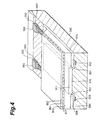
- Fig. 4 is a configurational view showing a back irradiation type light-receiving device using the technique of the conventional example.
- this device comprises: (a) a semiconductor thin plate 910 mainly composed of silicon, in which a charge coupled device (CCD), as a charge-reading section 911, is formed on its front side 916; (b) a field oxide film 920 formed around the charge-reading section 911; (c) polysilicon leads 931 formed on the charge-reading section 911 and at peripheral portions of the charge-reading section 911 on a front side 926 of the field oxide film 920; (d) polysilicon electrodes 932 formed on regions separated by the field oxide film 920 from the region where the charge-reading section 911 is formed; (e) metal leads 933 electrically connecting the polysilicon leads 931 with their corresponding polysilicon electrodes 932; (f) a reinforcement member 940 made of borosilicate glass deposited on the front side 916 of the semiconductor thin plate 910 and on the front side 926
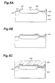
- FIGs. 5A to 5F are views showing, step by step, a method of making the back irradiation type light-receiving device in accordance with the conventional example.
- the charge-reading section 911 is formed on a semiconductor substrate 919.
- the field oxide film 920 is formed on a semiconductor substrate 919.
- the polysilicon leads 931 and the polysilicon electrodes 932 are formed (see Fig. 5A).
- the metal leads 933 for electrically connecting the polysilicon leads 931 to their corresponding polysilicon electrodes 932 are formed (see Fig. 5B).
- borosilicate glass is deposited on a surface constituted by the front side 916 of the semiconductor substrate 916 and the front side 926 of the field oxide film 920, so as to form the reinforcement member 940 (see Fig. 5C).
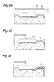
- the semiconductor substrate 919 is thinned so as to form the semiconductor thin plate 910.
- the protective oxide film 952 it is activated by ion injection and heating, thus forming the accumulation layer 951 (see Fig. 5D).
- a portion surrounding the charge-reading section 911 is removed by etching so as to expose the polysilicon electrodes 932 (see Fig. 5E).
- the metal electrodes 960 are formed on the polysilicon electrodes 932 so as to become bonding pads (see Fig. 5F). Thereafter, the bonding pads are subjected to wire bonding, thus yielding the back irradiation type light-receiving device shown in Fig. 4.
- the metal leads 933 held between the semiconductor thin plate 910 and the reinforcement member 940 are heated at a high temperature during the manufacturing steps, i.e., in the heat treatment (850°C to 900°C) at the time of sintering borosilicate glass when the reinforcement member 940 is formed, in the heat treatment (800°C to 900°C) at the time when the protective oxide film is grown, and in the high-temperature annealing (800°C to 900°C) after ion injection.
- US Patent US 4,870,475 discloses a method of manufacturing a semiconductor device.
- European patent EP 0314334 discloses an integrated circuit with an isolating feature.
- Japanese patent JP 06326293 discloses a rear irradiation type photodetector.
- Document EP-A-0 555 907 discloses a large area active matrix detector.
- metal leads 933 aluminum whose melting point is about 660°C cannot be used, and high-melting metals such as molybdenum and tungsten or their silicides are used.
- the currently-available high-melting metals or their silicides, high-melting metals in particular, are disadvantageous, as compared with aluminum, in terms of adhesiveness to its base, dry-etching characteristic, and property of reducing natural oxide films at the contact portion. Accordingly, it is difficult for them to stably proceed with the process as in the case where aluminum is used.
- the adhesiveness to the base and the dry-etching characteristic are better than those in the high-melting metals themselves. Nevertheless, the wiring resistance becomes higher when the silicides of high-melting metals are used.
- Astronomical light-receiving devices necessitate a large light-receiving area, whereby their wiring length increases. For example, assuming that the size of one pixel is 12 ⁇ m ⁇ 12 ⁇ m while 2,048 pixels and 4,096 pixels are respectively arranged in horizontal and vertical directions, the chip size is as large as about 2.5 cm in the horizontal direction and about 5 cm in the vertical direction.
- the wiring length of the high-melting metal in the vertical direction may be as long as about 5 cm.
- a typical sheet resistance of wiring made of a silicide of a high-melting metal is 0.5 ⁇ ⁇ . Accordingly, assuming that a vertical lead has a width of 20 ⁇ m and a length of 5 cm, its wiring resistance becomes as high as 1,250 ⁇ . Assuming that the wiring capacity is 40 nF, the CR time constant becomes as large as 50 ⁇ s, thus making it difficult to operate at high speed.
- the back irradiation type light-receiving device in accordance with the present invention is a back irradiation type light-receiving device, in which a charge-reading section having a one-dimensional or two-dimensional arrangement is formed on a first surface of a semiconductor thin plate mainly composed of silicon, for detecting an energy of an electromagnetic wave or charged particle incident on a second surface of the semiconductor thin plate which is a back side of the first surface, the device comprising: (a) a reinforcement substrate disposed on the first surface side of the semiconductor thin plate; (b) a field oxide film, formed in contact with the reinforcement substrate around a region where the charge-reading section is formed, exposing a surface thereof opposing an interface with respect to the reinforcement substrate while excluding at least a peripheral portion of the charge-reading section; (c) a polysilicon lead formed on the charge-reading section and at a region extending from the charge-reading section at the interface between the field oxide film and the reinforcement substrate to the exposed region of the field oxide film; the light receiving device character
- the reinforcement substrate one of borosilicate glass and borophosphosilicate glass may preferably be employed.
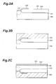
- Fig. 1 is a configurational view showing the back irradiation type light-receiving device in accordance with an embodiment of the present invention.
- this light-receiving device comprises: (a) a semiconductor thin plate 100, mainly composed of silicon, having a charge-reading section 110 on its surface 101 side; (b) a field oxide film 200, formed around a region where the charge-reading section 110 is formed, exposing a surface 202 except for the charge-reading section 110 and having contact holes 205 in the exposed region; (c) polysilicon leads 300 formed on the charge-reading section 110 and on a region extending to a region where the contact hole 205 is formed on a surface 201 of the field oxide film 200; (c) a reinforcement member 400 disposed on the surface 201 of the field oxide film 200 on the surface 101 of the semiconductor thin plate 101; (d) an accumulation layer 510 formed on a surface 102 of the semiconductor thin plate 100; (e) a protective oxide film 520 formed on the accumulation layer 510;
- borosilicate glass (BSG) or borophosphosilicate glass (BPSG) can preferably be employed as the reinforcement member.
- Figs. 2A to 2F are views showing, step by step, a method of making the back irradiation type light-receiving device in accordance with this embodiment.
- the charge-reading section 110 is formed on the surface 101 of a semiconductor substrate 190 mainly composed of silicon. Then, the field oxide film 200 is formed on the surface 101 of the semiconductor substrate 190 around the charge-reading section 110. Thereafter, the polysilicon leads 300 are selectively formed on the charge-reading section 110 and on the surface 201 of the field oxide film 200 (see Fig. 2A).
- the reinforcement member 400 is disposed on the surface 101 of the semiconductor substrate 190 and on the surface 201 of the field oxide film 200 (see Fig. 2B).
- BSG or BPSG can preferably be employed.
- a glass body made of BSG or BPSG may be attached to the above-mentioned surfaces by means of an adhesive or, as in the prior art, BSG may be deposited and sintered thereon.
- the semiconductor substrate 190 is processed so as to become the semiconductor thin plate 100.
- the protective oxide film 520 is formed on the surface 102 of the semiconductor thin plate 100, ions are injected therein from the surface 102 side thereof so as to activate it, thereby forming the accumulation layer 510 (see Fig. 2C).
- the constituent material of the semiconductor thin plate 100 is eliminated from the region other than regions constituted by the region where the charge-reading section 110 is formed and the region in the vicinity of the charge-reading section 110, thereby exposing the field oxide film 200 (see Fig. 2D), and the contact holes 205 communicating with their corresponding polysilicon leads 300 are formed at the exposed region of the field oxide film 200 (see Fig. 2E).
- the aluminum leads 600 (including the bonding pad portions 610) electrically connecting with their corresponding polysilicon leads 300 are formed. Thereafter, the bonding pad portions 610 are subjected to wire bonding, thus yielding the back irradiation type light-receiving device of this embodiment (see Fig. 2F).
- aluminum-wiring technique which is an established technique in the conventional semiconductor art, can be used to form the aluminum leads 600.
- those made of aluminum-silicon compounds; compounds of aluminum, silicon, and titanium; or various kinds of alloys or compounds based on aluminum may be used.
- the contact holes are formed in the field oxide film so as to physically and electrically direct-connect the aluminum leads to their corresponding polysilicon leads in the above mentioned embodiment, without being restricted thereto, the polysilicon leads may be exposed on the first surface side so as to be connected to their corresponding aluminium leads.
Landscapes
- Solid State Image Pick-Up Elements (AREA)
- Light Receiving Elements (AREA)
- Transforming Light Signals Into Electric Signals (AREA)
Claims (3)
- Dispositif photorécepteur de type à éclairement par face arrière, dans lequel une section de lecture de charge (110) ayant un agencement unidimensionnel ou bidimensionnel est formée sur une première surface d'une plaque mince semi-conductrice (100) principalement composée de silicium, destiné à détecter une énergie issue d'un incident d'onde électromagnétique ou de particules chargées sur une seconde surface de ladite plaque mince semi-conductrice (100), ladite seconde surface étant une face arrière de ladite première surface, ledit dispositif comprenant :un substrat de renforcement (400) disposé sur ladite première face de surface de ladite plaque mince semi-conductrice 100 ;une couche d'oxyde de champ (200), formée en contact avec ledit substrat de renforcement (400) autour d'une région où ladite section de lecture de charge (110) est formée, exposant une surface de cette dernière opposée à une interface par rapport audit substrat de renforcement (400) tout en excluant au moins une partie périphérique de ladite section de lecture de charge (110) ;une charge de polysilicone (300) formée sur ladite section de lecture de charge (110) et à une région s'étendant à partir de ladite section de lecture de charge (110) au niveau de l'interface entre ladite couche d'oxyde de champ (200) et ledit substrat de renforcement (400) jusqu'à la région exposée de ladite couche d'oxyde de champ (200), ledit dispositif photorécepteur ayant en outre,une charge métallique (600) faite en aluminium ou un alliage ou un composé d'aluminium, formée sur la région exposée de ladite couche d'oxyde de champ (200), ladite charge métallique (600) ayant une partie de plot de connexion (610) pour une connexion externe sur ladite première face de surface ; ledit dispositif étant caractérisé en ce que ladite charge métallique est physiquement et électriquement connectée directement à ladite charge de polysilicone (300) et en ce que ledit dispositif a quatre arêtes,dans lequel la partie de plot de connexion (610) est située adjacente à une seule des arêtes de façon à permettre audit dispositif de venir buter contre un dispositif supplémentaire sur l'une des trois autres arêtes.
- Dispositif photorécepteur de type à éclairement par face arrière selon la revendication 1, dans lequel ledit substrat de renforcement comprend l'un parmi le verre de borosilicate ou le verre de borophosphosilicate.
- Matrice de dispositifs photorécepteurs de type à éclairement par face arrière selon la revendication 1.
Applications Claiming Priority (2)
| Application Number | Priority Date | Filing Date | Title |
|---|---|---|---|
| JP270006/96 | 1996-10-11 | ||
| JP27000696A JP3620936B2 (ja) | 1996-10-11 | 1996-10-11 | 裏面照射型受光デバイスおよびその製造方法 |
Publications (3)
| Publication Number | Publication Date |
|---|---|
| EP0836231A2 EP0836231A2 (fr) | 1998-04-15 |
| EP0836231A3 EP0836231A3 (fr) | 1998-11-11 |
| EP0836231B1 true EP0836231B1 (fr) | 2007-03-21 |
Family
ID=17480247
Family Applications (1)
| Application Number | Title | Priority Date | Filing Date |
|---|---|---|---|
| EP97308026A Expired - Lifetime EP0836231B1 (fr) | 1996-10-11 | 1997-10-10 | Procédé de fabrication d'un dispositif photorécepteur de type à éclairement par face arrière |
Country Status (4)
| Country | Link |
|---|---|
| US (1) | US6031274A (fr) |
| EP (1) | EP0836231B1 (fr) |
| JP (1) | JP3620936B2 (fr) |
| DE (1) | DE69737492T2 (fr) |
Families Citing this family (27)
| Publication number | Priority date | Publication date | Assignee | Title |
|---|---|---|---|---|
| JP4373695B2 (ja) * | 2003-04-16 | 2009-11-25 | 浜松ホトニクス株式会社 | 裏面照射型光検出装置の製造方法 |
| US7829438B2 (en) | 2006-10-10 | 2010-11-09 | Tessera, Inc. | Edge connect wafer level stacking |
| US7901989B2 (en) | 2006-10-10 | 2011-03-08 | Tessera, Inc. | Reconstituted wafer level stacking |
| US8513789B2 (en) * | 2006-10-10 | 2013-08-20 | Tessera, Inc. | Edge connect wafer level stacking with leads extending along edges |
| US7791199B2 (en) * | 2006-11-22 | 2010-09-07 | Tessera, Inc. | Packaged semiconductor chips |
| US8569876B2 (en) | 2006-11-22 | 2013-10-29 | Tessera, Inc. | Packaged semiconductor chips with array |
| US7952195B2 (en) * | 2006-12-28 | 2011-05-31 | Tessera, Inc. | Stacked packages with bridging traces |
| EP2135280A2 (fr) * | 2007-03-05 | 2009-12-23 | Tessera, Inc. | Puces ayant des contacts arrière reliés par des trous de passage à des contacts avant |
| CN101809739B (zh) * | 2007-07-27 | 2014-08-20 | 泰塞拉公司 | 具有后应用的衬垫延长部分的重构晶片堆封装 |
| KR101538648B1 (ko) * | 2007-07-31 | 2015-07-22 | 인벤사스 코포레이션 | 실리콘 쓰루 비아를 사용하는 반도체 패키지 공정 |
| WO2009020572A2 (fr) | 2007-08-03 | 2009-02-12 | Tessera Technologies Hungary Kft. | Ensembles empilés utilisant des tranches reconstituées |
| US8043895B2 (en) * | 2007-08-09 | 2011-10-25 | Tessera, Inc. | Method of fabricating stacked assembly including plurality of stacked microelectronic elements |
| US20100053407A1 (en) * | 2008-02-26 | 2010-03-04 | Tessera, Inc. | Wafer level compliant packages for rear-face illuminated solid state image sensors |
| US20090212381A1 (en) * | 2008-02-26 | 2009-08-27 | Tessera, Inc. | Wafer level packages for rear-face illuminated solid state image sensors |
| JP5639052B2 (ja) * | 2008-06-16 | 2014-12-10 | テッセラ,インコーポレイテッド | ウェハレベルでの縁部の積重ね |
| US8466542B2 (en) * | 2009-03-13 | 2013-06-18 | Tessera, Inc. | Stacked microelectronic assemblies having vias extending through bond pads |
| US9640437B2 (en) | 2010-07-23 | 2017-05-02 | Tessera, Inc. | Methods of forming semiconductor elements using micro-abrasive particle stream |
| US8796135B2 (en) | 2010-07-23 | 2014-08-05 | Tessera, Inc. | Microelectronic elements with rear contacts connected with via first or via middle structures |
| US8791575B2 (en) | 2010-07-23 | 2014-07-29 | Tessera, Inc. | Microelectronic elements having metallic pads overlying vias |
| US8610259B2 (en) | 2010-09-17 | 2013-12-17 | Tessera, Inc. | Multi-function and shielded 3D interconnects |
| US8847380B2 (en) | 2010-09-17 | 2014-09-30 | Tessera, Inc. | Staged via formation from both sides of chip |
| KR101059490B1 (ko) | 2010-11-15 | 2011-08-25 | 테세라 리써치 엘엘씨 | 임베드된 트레이스에 의해 구성된 전도성 패드 |
| US8587126B2 (en) | 2010-12-02 | 2013-11-19 | Tessera, Inc. | Stacked microelectronic assembly with TSVs formed in stages with plural active chips |
| US8736066B2 (en) | 2010-12-02 | 2014-05-27 | Tessera, Inc. | Stacked microelectronic assemby with TSVS formed in stages and carrier above chip |
| US8637968B2 (en) | 2010-12-02 | 2014-01-28 | Tessera, Inc. | Stacked microelectronic assembly having interposer connecting active chips |
| US8610264B2 (en) | 2010-12-08 | 2013-12-17 | Tessera, Inc. | Compliant interconnects in wafers |
| JP7822790B2 (ja) * | 2022-01-05 | 2026-03-03 | キヤノン株式会社 | 光電変換装置 |
Citations (1)
| Publication number | Priority date | Publication date | Assignee | Title |
|---|---|---|---|---|
| EP0762504A2 (fr) * | 1995-09-05 | 1997-03-12 | Canon Kabushiki Kaisha | Convertisseur photoélectrique |
Family Cites Families (5)
| Publication number | Priority date | Publication date | Assignee | Title |
|---|---|---|---|---|
| JPS54110068U (fr) * | 1978-01-20 | 1979-08-02 | ||
| US4870475A (en) * | 1985-11-01 | 1989-09-26 | Nec Corporation | Semiconductor device and method of manufacturing the same |
| US4892842A (en) * | 1987-10-29 | 1990-01-09 | Tektronix, Inc. | Method of treating an integrated circuit |
| US4923825A (en) * | 1989-05-01 | 1990-05-08 | Tektronix, Inc. | Method of treating a semiconductor body |
| JPH06326293A (ja) * | 1993-05-12 | 1994-11-25 | Hamamatsu Photonics Kk | 光検出装置 |
-
1996
- 1996-10-11 JP JP27000696A patent/JP3620936B2/ja not_active Expired - Lifetime
-
1997
- 1997-10-10 DE DE69737492T patent/DE69737492T2/de not_active Expired - Lifetime
- 1997-10-10 EP EP97308026A patent/EP0836231B1/fr not_active Expired - Lifetime
- 1997-10-10 US US08/948,822 patent/US6031274A/en not_active Expired - Lifetime
Patent Citations (1)
| Publication number | Priority date | Publication date | Assignee | Title |
|---|---|---|---|---|
| EP0762504A2 (fr) * | 1995-09-05 | 1997-03-12 | Canon Kabushiki Kaisha | Convertisseur photoélectrique |
Also Published As
| Publication number | Publication date |
|---|---|
| DE69737492T2 (de) | 2007-11-29 |
| JP3620936B2 (ja) | 2005-02-16 |
| JPH10116974A (ja) | 1998-05-06 |
| US6031274A (en) | 2000-02-29 |
| DE69737492D1 (de) | 2007-05-03 |
| EP0836231A3 (fr) | 1998-11-11 |
| EP0836231A2 (fr) | 1998-04-15 |
Similar Documents
| Publication | Publication Date | Title |
|---|---|---|
| EP0836231B1 (fr) | Procédé de fabrication d'un dispositif photorécepteur de type à éclairement par face arrière | |
| US6204506B1 (en) | Back illuminated photodetector and method of fabricating the same | |
| JP5185205B2 (ja) | 半導体光検出素子 | |
| EP0616373A2 (fr) | Dispositif semi-conducteur de conversion photoélectrique et méthode de fabrication | |
| US6504178B2 (en) | Indirect back surface contact to semiconductor devices | |
| US5670817A (en) | Monolithic-hybrid radiation detector/readout | |
| CA1291554C (fr) | Dispositif semiconducteur radiosensible | |
| US20120298175A1 (en) | Solar panel module and method for manufacturing such a solar panel module | |
| JP5829224B2 (ja) | Mosイメージセンサ | |
| US7810740B2 (en) | Back illuminated photodiode array, manufacturing method and semiconductor device thereof | |
| JP2797984B2 (ja) | 固体撮像素子およびその製造方法 | |
| EP1280207A1 (fr) | Detecteur d'energie a semi-conducteur | |
| EP1569275B1 (fr) | Reseau de photodiodes a retroeclairage, procede de fabrication de celui-ci et dispositif semi-conducteur | |
| JP4522531B2 (ja) | 半導体エネルギー検出素子 | |
| WO2021131758A1 (fr) | Photodétecteur à semi-conducteur | |
| CN114300494B (zh) | 一种光电二极管、光电二极管探测器及其制造方法 | |
| JP2651323B2 (ja) | 半導体エネルギー検出器 | |
| CN100438080C (zh) | 具有一个或多个导电触点的辐射检测器及其制造方法 | |
| JP2019512890A (ja) | 直接読み取りピクセルアライメント | |
| JPH06326293A (ja) | 光検出装置 | |
| JP2005520346A (ja) | 画素センサーのアレーとその製造方法 | |
| US4148052A (en) | Radiant energy sensor | |
| JP2897745B2 (ja) | 固体撮像素子およびその製造方法 | |
| JP2997141B2 (ja) | 太陽電池 |
Legal Events
| Date | Code | Title | Description |
|---|---|---|---|
| PUAI | Public reference made under article 153(3) epc to a published international application that has entered the european phase |
Free format text: ORIGINAL CODE: 0009012 |
|
| AK | Designated contracting states |
Kind code of ref document: A2 Designated state(s): DE FR GB |
|
| RIN1 | Information on inventor provided before grant (corrected) |
Inventor name: AKAHORI, HIROSHI Inventor name: MURAMATSU, MASAHARU |
|
| PUAL | Search report despatched |
Free format text: ORIGINAL CODE: 0009013 |
|
| AK | Designated contracting states |
Kind code of ref document: A3 Designated state(s): AT BE CH DE DK ES FI FR GB GR IE IT LI LU MC NL PT SE |
|
| 17P | Request for examination filed |
Effective date: 19990505 |
|
| AKX | Designation fees paid |
Free format text: DE FR GB |
|
| 17Q | First examination report despatched |
Effective date: 20021205 |
|
| GRAP | Despatch of communication of intention to grant a patent |
Free format text: ORIGINAL CODE: EPIDOSNIGR1 |
|
| RTI1 | Title (correction) |
Free format text: METHOD OF MAKING A BACK IRRADIATION TYPE LIGHT-RECEIVING DEVICE |
|
| GRAJ | Information related to disapproval of communication of intention to grant by the applicant or resumption of examination proceedings by the epo deleted |
Free format text: ORIGINAL CODE: EPIDOSDIGR1 |
|
| GRAP | Despatch of communication of intention to grant a patent |
Free format text: ORIGINAL CODE: EPIDOSNIGR1 |
|
| GRAS | Grant fee paid |
Free format text: ORIGINAL CODE: EPIDOSNIGR3 |
|
| GRAA | (expected) grant |
Free format text: ORIGINAL CODE: 0009210 |
|
| AK | Designated contracting states |
Kind code of ref document: B1 Designated state(s): DE FR GB |
|
| REG | Reference to a national code |
Ref country code: GB Ref legal event code: FG4D |
|
| REF | Corresponds to: |
Ref document number: 69737492 Country of ref document: DE Date of ref document: 20070503 Kind code of ref document: P |
|
| ET | Fr: translation filed | ||
| PLBE | No opposition filed within time limit |
Free format text: ORIGINAL CODE: 0009261 |
|
| STAA | Information on the status of an ep patent application or granted ep patent |
Free format text: STATUS: NO OPPOSITION FILED WITHIN TIME LIMIT |
|
| 26N | No opposition filed |
Effective date: 20071227 |
|
| REG | Reference to a national code |
Ref country code: FR Ref legal event code: PLFP Year of fee payment: 20 |
|
| REG | Reference to a national code |
Ref country code: DE Ref legal event code: R082 Ref document number: 69737492 Country of ref document: DE Representative=s name: MAUCHER JENKINS, DE |
|
| PGFP | Annual fee paid to national office [announced via postgrant information from national office to epo] |
Ref country code: FR Payment date: 20160919 Year of fee payment: 20 |
|
| PGFP | Annual fee paid to national office [announced via postgrant information from national office to epo] |
Ref country code: DE Payment date: 20161004 Year of fee payment: 20 Ref country code: GB Payment date: 20161005 Year of fee payment: 20 |
|
| REG | Reference to a national code |
Ref country code: DE Ref legal event code: R071 Ref document number: 69737492 Country of ref document: DE |
|
| REG | Reference to a national code |
Ref country code: GB Ref legal event code: PE20 Expiry date: 20171009 |
|
| PG25 | Lapsed in a contracting state [announced via postgrant information from national office to epo] |
Ref country code: GB Free format text: LAPSE BECAUSE OF EXPIRATION OF PROTECTION Effective date: 20171009 |