EP0836372A2 - Méthode et appareil de création d'une surface d'aspiration sur un objet et composant électrique fabriqué ainsi - Google Patents
Méthode et appareil de création d'une surface d'aspiration sur un objet et composant électrique fabriqué ainsi Download PDFInfo
- Publication number
- EP0836372A2 EP0836372A2 EP97117153A EP97117153A EP0836372A2 EP 0836372 A2 EP0836372 A2 EP 0836372A2 EP 97117153 A EP97117153 A EP 97117153A EP 97117153 A EP97117153 A EP 97117153A EP 0836372 A2 EP0836372 A2 EP 0836372A2
- Authority
- EP
- European Patent Office
- Prior art keywords
- shroud
- adhesive mass
- suction surface
- radiation
- module
- Prior art date
- Legal status (The legal status is an assumption and is not a legal conclusion. Google has not performed a legal analysis and makes no representation as to the accuracy of the status listed.)
- Ceased
Links
Images

Classifications
-
- H—ELECTRICITY
- H01—ELECTRIC ELEMENTS
- H01G—CAPACITORS; CAPACITORS, RECTIFIERS, DETECTORS, SWITCHING DEVICES, LIGHT-SENSITIVE OR TEMPERATURE-SENSITIVE DEVICES OF THE ELECTROLYTIC TYPE
- H01G2/00—Details of capacitors not covered by a single one of groups H01G4/00-H01G11/00
- H01G2/02—Mountings
- H01G2/06—Mountings specially adapted for mounting on a printed-circuit support
- H01G2/065—Mountings specially adapted for mounting on a printed-circuit support for surface mounting, e.g. chip capacitors
-
- H—ELECTRICITY
- H05—ELECTRIC TECHNIQUES NOT OTHERWISE PROVIDED FOR
- H05K—PRINTED CIRCUITS; CASINGS OR CONSTRUCTIONAL DETAILS OF ELECTRIC APPARATUS; MANUFACTURE OF ASSEMBLAGES OF ELECTRICAL COMPONENTS
- H05K13/00—Apparatus or processes specially adapted for manufacturing or adjusting assemblages of electric components
- H05K13/02—Feeding of components
- H05K13/021—Loading or unloading of containers
-
- H—ELECTRICITY
- H05—ELECTRIC TECHNIQUES NOT OTHERWISE PROVIDED FOR
- H05K—PRINTED CIRCUITS; CASINGS OR CONSTRUCTIONAL DETAILS OF ELECTRIC APPARATUS; MANUFACTURE OF ASSEMBLAGES OF ELECTRICAL COMPONENTS
- H05K13/00—Apparatus or processes specially adapted for manufacturing or adjusting assemblages of electric components
- H05K13/04—Mounting of components, e.g. of leadless components
- H05K13/0417—Feeding with belts or tapes
-
- H—ELECTRICITY
- H05—ELECTRIC TECHNIQUES NOT OTHERWISE PROVIDED FOR
- H05K—PRINTED CIRCUITS; CASINGS OR CONSTRUCTIONAL DETAILS OF ELECTRIC APPARATUS; MANUFACTURE OF ASSEMBLAGES OF ELECTRICAL COMPONENTS
- H05K13/00—Apparatus or processes specially adapted for manufacturing or adjusting assemblages of electric components
- H05K13/04—Mounting of components, e.g. of leadless components
- H05K13/046—Surface mounting
-
- H—ELECTRICITY
- H05—ELECTRIC TECHNIQUES NOT OTHERWISE PROVIDED FOR
- H05K—PRINTED CIRCUITS; CASINGS OR CONSTRUCTIONAL DETAILS OF ELECTRIC APPARATUS; MANUFACTURE OF ASSEMBLAGES OF ELECTRICAL COMPONENTS
- H05K3/00—Apparatus or processes for manufacturing printed circuits
- H05K3/30—Assembling printed circuits with electric components, e.g. with resistors
- H05K3/303—Assembling printed circuits with electric components, e.g. with resistors with surface mounted components
-
- H—ELECTRICITY
- H05—ELECTRIC TECHNIQUES NOT OTHERWISE PROVIDED FOR
- H05K—PRINTED CIRCUITS; CASINGS OR CONSTRUCTIONAL DETAILS OF ELECTRIC APPARATUS; MANUFACTURE OF ASSEMBLAGES OF ELECTRICAL COMPONENTS
- H05K2201/00—Indexing scheme relating to printed circuits covered by H05K1/00
- H05K2201/10—Details of components or other objects attached to or integrated in a printed circuit board
- H05K2201/10431—Details of mounted components
- H05K2201/10583—Cylindrically shaped component; Fixing means therefore
-
- H—ELECTRICITY
- H05—ELECTRIC TECHNIQUES NOT OTHERWISE PROVIDED FOR
- H05K—PRINTED CIRCUITS; CASINGS OR CONSTRUCTIONAL DETAILS OF ELECTRIC APPARATUS; MANUFACTURE OF ASSEMBLAGES OF ELECTRICAL COMPONENTS
- H05K2201/00—Indexing scheme relating to printed circuits covered by H05K1/00
- H05K2201/10—Details of components or other objects attached to or integrated in a printed circuit board
- H05K2201/10613—Details of electrical connections of non-printed components, e.g. special leads
- H05K2201/10621—Components characterised by their electrical contacts
- H05K2201/10651—Component having two leads, e.g. resistor, capacitor
-
- H—ELECTRICITY
- H05—ELECTRIC TECHNIQUES NOT OTHERWISE PROVIDED FOR
- H05K—PRINTED CIRCUITS; CASINGS OR CONSTRUCTIONAL DETAILS OF ELECTRIC APPARATUS; MANUFACTURE OF ASSEMBLAGES OF ELECTRICAL COMPONENTS
- H05K2203/00—Indexing scheme relating to apparatus or processes for manufacturing printed circuits covered by H05K3/00
- H05K2203/01—Tools for processing; Objects used during processing
- H05K2203/0195—Tool for a process not provided for in H05K3/00, e.g. tool for handling objects using suction, for deforming objects, for applying local pressure
-
- H—ELECTRICITY
- H05—ELECTRIC TECHNIQUES NOT OTHERWISE PROVIDED FOR
- H05K—PRINTED CIRCUITS; CASINGS OR CONSTRUCTIONAL DETAILS OF ELECTRIC APPARATUS; MANUFACTURE OF ASSEMBLAGES OF ELECTRICAL COMPONENTS
- H05K2203/00—Indexing scheme relating to apparatus or processes for manufacturing printed circuits covered by H05K3/00
- H05K2203/08—Treatments involving gases
- H05K2203/082—Suction, e.g. for holding solder balls or components
-
- Y—GENERAL TAGGING OF NEW TECHNOLOGICAL DEVELOPMENTS; GENERAL TAGGING OF CROSS-SECTIONAL TECHNOLOGIES SPANNING OVER SEVERAL SECTIONS OF THE IPC; TECHNICAL SUBJECTS COVERED BY FORMER USPC CROSS-REFERENCE ART COLLECTIONS [XRACs] AND DIGESTS
- Y02—TECHNOLOGIES OR APPLICATIONS FOR MITIGATION OR ADAPTATION AGAINST CLIMATE CHANGE
- Y02P—CLIMATE CHANGE MITIGATION TECHNOLOGIES IN THE PRODUCTION OR PROCESSING OF GOODS
- Y02P70/00—Climate change mitigation technologies in the production process for final industrial or consumer products
- Y02P70/50—Manufacturing or production processes characterised by the final manufactured product
Definitions
- the invention relates to a method for manufacturing a suction surface on an object that is preferably an electrical one intended for SMD assembly technology Component is, the suction surface on one of the mounting side opposite surface of the in a delivery module present object is arranged. Furthermore, the invention relates to a device for Carrying out this procedure and a formed with it electrical component, as well as a supply module in one Blister belt.
- the components used often have a substantially cylindrical shape, such as Example resistors, a spiral shape, such as Example electrical coils, and others from a flat one Different shapes. Therefore often an exact recording by the suction pipette is not possible.
- German utility model suggests DE-GM 94 10 532 the attachment of a plate on the top of the component.
- This tile will attached to the component by an adhesive and is arranged that on the opposite side of the mounting side Surface of the electrical component is a flat surface.
- the components designed in this way can be the suction pipette are correctly picked up, however, require complex assembly of the electrical component with the tiles. There is an additional processing step for this necessary to be executed very precisely must and therefore a high expenditure on device technology with, corresponding time required.
- the invention is therefore based on the object Method and device for producing a suction surface to point to an object by means of the or a flat surface on the component in a simple manner can be trained.
- this task is solved by that after the correct insertion of the object an adhesive mass in the preparation module the top of the item is applied, a shroud is placed over the adhesive mass, and a stamp so exerts pressure on the shroud that is on a plane of the adhesive mass underneath Suction surface is created.
- this object is also achieved by a metering device for applying a predetermined Amount of an adhesive mass on the in one Provisioning module in the correct position, a device for arranging a shroud over the adhesive mass, and a stamp with the through the cover tape to the adhesive below Mass a flat suction surface can be pressed.
- the objects can therefore advantageously be used in a Equipped in spite of their small dimensions also in the Mass production reliably started and for example transported to a circuit board and exactly positioned there will.
- Another advantage is that the components for application the adhesive mass not from the delivery module have to be removed, because these by the Dosing device made in a precisely controlled manner can be.
- the method according to the invention and the corresponding one Device can advantageously be easily involved in the manufacturing process of such items will. This is a continuous prefabrication of electrical components possible in mass production.
- the fact that the adhesive mass by a corresponding Hardening device is cured, the Hardening process of the adhesive connection is effectively accelerated will.
- the hardening is thereby preferably by exposure to energy electromagnetic radiation, especially light in the visible area. So that the radiation on the adhesive mass arranged under the shroud can act, the cover band is transparent to radiation educated. This can be easily done under Effective use of known radiation technologies Curing can be achieved.
- the objects lie with the flat suction surface individually and in a reusable state in the delivery module in front.
- the fact that one of several delivery modules formed blister belt is used is a continuous one Production of the component according to the invention possible.
- the blister belt enables components to pass through by the device according to the invention and thereby reduced the design effort for the device.
- a component preferably an electrical component is shown, which is a formed by the inventive method has a flat suction surface.
- This component is there advantageous that it is less in contrast to the prior art Has components and therefore easier to manufacture is. It also allows the desired secure recording, reliable transport and precise positioning the component by means of a pipette or the like. The Component can therefore be fully automated on a circuit board be equipped.
- a Provisioning module especially created in a blister belt, which is a preferably selective marking layer has on the shroud.
- This label layer gives the user information that the object has a flat suction surface in the blister belt, which was produced by the method according to the invention. This makes the item suitable for automatic placement recognizable in the blister belt.
- this marking layer during manufacture the flat suction surface on the object preferably inevitably due to residues of the cured adhesive Mass is formed. A separate identification on the blister belt is therefore not necessary.
- FIGs 1 and 2 is an electrical component shown, which is exemplary for the multitude of possible applications the invention can be seen.
- a choke coil 1 is shown in the figures essentially cylindrical main body 2 and connecting wires 3 and 4. Furthermore, there is a mounting side 5 opposite a flat suction surface 6 am Main body 2 of the throttle 1 is formed.
- This choke coil 1 is therefore suitable from one Suction pipette, not shown, sucked in a known manner, recorded and to a circuit board or the like to be transported and placed there exactly.
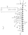
- the chokes 1 in a known manner, for example by a vibrating or The screw conveyor is correctly oriented in one position Blister belt formed from several preparation modules 10 8 arranged.
- the blister belt 8 has a blister body 11 with recesses 12 for receiving the chokes 1 on.
- the blister belt 8 moves in the direction of Arrow 15 progressively.
- a metering device 20 is provided below, around an adhesive mass 21 in a precisely controlled manner on the surface opposite the mounting side 5 to apply the throttle 1.
- the amount of adhesive Mass is chosen so that a sufficiently large plane suction surface 6 are formed on the throttle 1 can. Depending on the shape and size of the component, the The amount of adhesive mass 21 therefore varies.
- a device 30 is used transparent shroud 13 over the chokes 1 and thus applied over the adhesive mass 21.
- the device 30 is a deflection roller in this embodiment, which, for example, the cover tape fed from a roll 13 deflected onto the blister belt 8.
- a stamp 40 is activated, which according to the representation in Fig. 3 vertical to the direction of the Blister belt 8 is movable back and forth.
- the progression the blister belt 8 is controlled so that the stamp 40 each over the adhesive mass 21 on the respective choke 1 comes to rest and the shroud 13 this point presses on the adhesive mass 21.
- the adhesive mass 21 thereby deforms and forms according to the shape of the flat end face 41 of the stamp 40 a flat surface.
- the shroud lies due to the adhesive force of the mass 21 13 thus glued to the respective throttle 1 before.
- the adhesive mass is subsequently represented by a Curing device 50 by applying radiation energy hardened.
- a Curing device 50 by applying radiation energy hardened.
- Fig. 3 there are two interacting elements the curing device 50 shown for a ensure sufficient curing distance with UV light.
- the shroud 13 is designed to be permeable to UV light.
- the scraper 60 has a hold-down device 61 and a scraper for this purpose 62 on. Between the hold-down device 61 and the wiper 62, the shroud 13 is upright with respect the direction of the blister belt 8 deflected and continued.
- the design of the scraper 62 and Hold-down device 61 ensures that the chokes 1 not to be lifted out of the blister belt 8.
- the mass 21 Since the mass 21 has already hardened, it retains her shape as a flat surface. Significant is that the materials of the cover tape 13 and the adhesive Mass 21 should be chosen so that the adhesive Mass 21 when stripping the shroud 13 on the Throttle 1 remains and only insignificant residues on Shroud 13 occur. Since the shroud 13 is made transparent is the residue of mass 21 on the shroud 13 recognizable and serve as a marking layer, which indicates that the object in the blister belt 8 according to the invention Process is designed and a plane Has suction surface.
- a shroud applicator 70 in Shape of a roll provided that the severed shroud 13 again on the blister belt 8.
- a Welding device 80 is finally with the shroud 13 the blister belt 8 welded, causing the respective chokes 1 effectively changed during transport becomes. Since the connection of the shroud 13 to the mass 21st was lifted by the stripping device 60 the chokes 1 thus loosely in the depressions of the blister belt 8 before.
- the adhesive mass 21 can also by a be cured according to the chosen additive so that the curing device 50 can be omitted.
- stripping device 60 it is also possible to use the stripping device 60 to do without and the separation between the shroud 13 and the mass 21 immediately before the chokes are fitted 1 to perform.
- This can also be any other way designed stripping device can be used which is just a reliable separation between the shroud 13 and the mass 21 must cause without the plane Design of the suction surface 6 significantly affected becomes.
- the stamp 40 can have any shape and Have control mode, but it should only be suitable must to deform the mass 21 so that it is on the surface forms a flat surface.
- the described method and the corresponding device can be used on electrical components of all kinds Shape and size can be applied. Furthermore it is also possible to use the method and the device for Example in the mechanical area for the formation of suction surfaces to be used on mostly small components for further transport to enable this. Special applications lie here in particular in an automated mechanical Assembly. Finally, the invention can be particularly apply in all cases where any Obtained subject of a certain surface shape must, for example, by a suction pipette or a other tool commonly used in assembly technology and can be reliably picked up and transported.
- a material can be used that is in a liquefy later processing after assembly, evaporate or let it evaporate. This is preferably done Liquefy or volatilize by heating the suction surface, at which the adhesive Mass liquefied or volatilized, but the solder or Fastening means for fastening the component on a Board or in a system remains fixed.
- volatilizing or liquefying material Wax, rosin and / or plastic which is in a Soldering temperature (reflow soldering) from, for example, 230 ° to 250 ° C evaporates or flows away. This gives you, for example a coil whose turns after soldering can be adjusted subsequently. It is also suitable such a material also for movable mechanical Components that are to be processed as SMD components whereby the mobility of the mechanical component is blocked Suction surface by heating or radiation can be volatilized or liquefied.
- Soldering temperature reflow soldering
- provisioning module 10 is also used.
- provision modules 10 are like e.g. Micropack feeds from the roll are known and familiar to the expert.
- the invention can Device also connected several times in parallel be arranged.
- the invention thus shows a method and an apparatus for producing a suction surface 6 on an object, preferably one for SMD assembly technology provided electrical component is. Furthermore, the Invention an electrical component 1 that on the mounting side 5 opposite surface a flat suction surface 6 has. This suction surface 6 is thereby trained that on the component 1 an adhesive Mass 21 applied and one arranged above Cover band 13 by means of a stamp 40 onto mass 21 is pressed that they plan to form one Deformed surface. After curing the adhesive Mass 21, the shroud 13 is separated from the mass 21 and there is a component 1 with a flat suction surface 6 which, for example, from a pipette reliable and sucked in easily, thereby absorbed and transported can be.
Landscapes
- Engineering & Computer Science (AREA)
- Microelectronics & Electronic Packaging (AREA)
- Power Engineering (AREA)
- Manufacturing & Machinery (AREA)
- Electric Connection Of Electric Components To Printed Circuits (AREA)
- Application Of Or Painting With Fluid Materials (AREA)
- Container, Conveyance, Adherence, Positioning, Of Wafer (AREA)
- Manipulator (AREA)
- Die Bonding (AREA)
- Supply And Installment Of Electrical Components (AREA)
Applications Claiming Priority (2)
| Application Number | Priority Date | Filing Date | Title |
|---|---|---|---|
| DE29617668U DE29617668U1 (de) | 1996-10-10 | 1996-10-10 | Vorrichtung zur Herstellung einer Ansaugfläche auf einem Gegenstand und dadurch ausgebildetes elektrisches Bauteil |
| DE29617668U | 1996-10-10 |
Publications (2)
| Publication Number | Publication Date |
|---|---|
| EP0836372A2 true EP0836372A2 (fr) | 1998-04-15 |
| EP0836372A3 EP0836372A3 (fr) | 1998-07-01 |
Family
ID=8030426
Family Applications (1)
| Application Number | Title | Priority Date | Filing Date |
|---|---|---|---|
| EP97117153A Ceased EP0836372A3 (fr) | 1996-10-10 | 1997-10-02 | Méthode et appareil de création d'une surface d'aspiration sur un objet et composant électrique fabriqué ainsi |
Country Status (3)
| Country | Link |
|---|---|
| US (1) | US6042683A (fr) |
| EP (1) | EP0836372A3 (fr) |
| DE (2) | DE29617668U1 (fr) |
Families Citing this family (8)
| Publication number | Priority date | Publication date | Assignee | Title |
|---|---|---|---|---|
| GB2320132A (en) * | 1996-12-04 | 1998-06-10 | Ibm | Handling electronic modules |
| DE19901962B4 (de) * | 1999-01-19 | 2006-05-11 | Erni Elektroapparate Gmbh | Verfahren zum Montieren elektrischer Steckverbindungen sowie Montagehilfe zur Verfahrensdurchführung |
| DE19956828C2 (de) * | 1999-11-25 | 2003-02-13 | Vogt Electronic Ag | Modifizierter Ringkern zur Verwendung in einem elektromagnetischen Bauelement |
| DE10059534C1 (de) | 2000-11-30 | 2002-06-27 | Epcos Ag | Elektrisches Bauelement, Anordnung des Bauelements und Verfahren zur Herstellung der Anordnung |
| US20030200100A1 (en) * | 2002-04-18 | 2003-10-23 | Say-Yee Wen | Method and reminding assignment deadlines |
| US7564336B2 (en) | 2004-08-26 | 2009-07-21 | Cooper Technologies Company | Surface mount magnetic core with coil termination clip |
| DE102005022927A1 (de) † | 2005-05-13 | 2006-11-16 | Würth Elektronik iBE GmbH | Elektronisches Bauteil und Verfahren zu seiner Befestigung |
| JP6467632B2 (ja) * | 2015-04-27 | 2019-02-13 | パナソニックIpマネジメント株式会社 | テープフィーダおよび部品実装装置 |
Family Cites Families (21)
| Publication number | Priority date | Publication date | Assignee | Title |
|---|---|---|---|---|
| DE3226733A1 (de) * | 1981-11-26 | 1983-07-07 | Softelec S.A., 1400 Yverdon | Integrierter schaltkreis |
| JPS60144298U (ja) * | 1984-03-05 | 1985-09-25 | 株式会社村田製作所 | チツプ型電子部品連 |
| DE8604096U1 (de) * | 1986-02-15 | 1986-04-24 | Vogt Electronic Ag, 94130 Obernzell | Induktivität in SMD-Technik |
| DE3615307C2 (de) * | 1986-05-06 | 1994-07-07 | Johann Leonhard Huettlinger | Spule für automatische SMD-Bestückung |
| JP2662948B2 (ja) * | 1986-10-30 | 1997-10-15 | ニツト− システム テクノロジ− インコ−ポレ−テツド | チップテープのトップテープ除去装置 |
| CA1322271C (fr) * | 1987-02-25 | 1993-09-21 | Sho Masujima | Ruban support pour elements de circuit electronique et methode de fabrication de series d'elements de circuit electronique |
| DE3710184A1 (de) * | 1987-03-27 | 1988-10-13 | Siemens Ag | Elektrisches bauelement |
| DE3806738C1 (fr) * | 1988-03-02 | 1989-09-07 | Espe Stiftung & Co Produktions- Und Vertriebs Kg, 8031 Seefeld, De | |
| WO1990013135A1 (fr) * | 1989-04-21 | 1990-11-01 | Motorola, Inc. | Inducteur sans fer ameliore pouvant etre monte sur une surface |
| DE4016698A1 (de) * | 1990-05-23 | 1991-11-28 | Siemens Ag | Hilfstraeger zum uebertragen von teilen auf einen traeger und verfahren zu dessen anwendung |
| DE4020305A1 (de) * | 1990-06-26 | 1992-01-09 | Siemens Ag | Spule zur oberflaechenmontage |
| DE4101790C1 (en) * | 1991-01-18 | 1992-07-09 | Technisch-Wissenschaftliche-Gesellschaft Thiede Und Partner Mbh, O-1530 Teltow, De | Chip-support arrangement prodn. - in tape form, in dual-in-line format by film-bond technology |
| DE4129146A1 (de) * | 1991-09-02 | 1993-03-04 | Siemens Nixdorf Inf Syst | Bandfoermiger hilfstraeger als montagehilfe fuer die zeilenweise montage von halbleiterchips auf einer passflaeche eines traegerelementes und ein zugehoeriges montageverfahren |
| EP0540497A3 (en) * | 1991-10-29 | 1993-06-16 | Alcatel Austria Aktiengesellschaft | Method of making solid solder coatings |
| JPH0810729B2 (ja) * | 1993-01-20 | 1996-01-31 | 日本電気株式会社 | 捺印機 |
| DE4309715C1 (de) * | 1993-03-25 | 1994-03-03 | Grundig Emv | Verfahren zum Abstimmen eines in SMD-Technik aufgebauten Schwingkreises |
| US5383797A (en) * | 1993-07-08 | 1995-01-24 | Molex Incorporated | System for handling electrical connectors by a vacuum-suction nozzle |
| JP3062517B2 (ja) * | 1993-09-17 | 2000-07-10 | 萩原エンジニアリング株式会社 | 物品整列装置 |
| JPH0817602A (ja) * | 1994-06-24 | 1996-01-19 | Matsushita Electric Ind Co Ltd | 面実装部品 |
| DE9410532U1 (de) * | 1994-06-29 | 1994-08-25 | Hagn, Erwin, 85368 Moosburg | Elektrisches Bauteil, insbesondere Spule, vorzugsweise für SMD-Montagetechnik |
| DE9420283U1 (de) * | 1994-12-19 | 1995-03-30 | Hagn, Erwin, 85368 Moosburg | Elektrisches Bauteil, insbesondere Spule, vorzugsweise für SMD-Montagetechnik |
-
1996
- 1996-10-10 DE DE29617668U patent/DE29617668U1/de not_active Expired - Lifetime
-
1997
- 1997-10-02 EP EP97117153A patent/EP0836372A3/fr not_active Ceased
- 1997-10-08 DE DE19744455A patent/DE19744455A1/de not_active Ceased
- 1997-10-10 US US08/948,423 patent/US6042683A/en not_active Expired - Fee Related
Also Published As
| Publication number | Publication date |
|---|---|
| DE19744455A1 (de) | 1998-04-16 |
| EP0836372A3 (fr) | 1998-07-01 |
| US6042683A (en) | 2000-03-28 |
| DE29617668U1 (de) | 1996-12-05 |
Similar Documents
| Publication | Publication Date | Title |
|---|---|---|
| EP0655020B1 (fr) | Procede et dispositif de metallisation d'une zone de contact | |
| DE3805572C2 (de) | Trägerband für elektronische Bauelemente sowie Verfahren zum Herstellen einer Folge von elektronischen Bauelementen | |
| DE112019005954T5 (de) | Schichtkernherstellungsverfahren, Klebstoffauftragseinrichtung und Schichtkernherstellungsapparat | |
| EP0392974A2 (fr) | Appareil pour appliquer mécaniquement des composites flexibles collant d'un côté sur des pièces à travailler, et leur utilisation | |
| DE2949196A1 (de) | Aufnahmevorrichtung fuer elektronische bauelemente in chip-form und verfahren zur serienweisen bereitstellung solcher bauelemente fuer fertigungsprozesse o.dgl. | |
| EP0726541A2 (fr) | Méthode pour la fabrication des cartes d'identité et carte d'identité produite par cette méthode | |
| EP0145832A2 (fr) | Procédé et appareil pour la fabrication d'un objet revêtu | |
| EP3316457A1 (fr) | Dispositif et procédé de liaison de parties de tôles à un paquet de tôles | |
| CH703698A1 (de) | Vorrichtung zum positionsgenauen Applizieren von Elementen auf eine Fläche eines Gegenstandes. | |
| DE3810285C2 (de) | Verfahren zum Bestücken einer Leiterplatte mit gegurteten und mit Klebstoff versehenen oberflächenmontierbaren Bauelementen (SMD) | |
| DE3913604A1 (de) | Verfahren und vorrichtung zum aufbringen von unterschriftsstreifen auf ausweiskarten | |
| EP0836372A2 (fr) | Méthode et appareil de création d'une surface d'aspiration sur un objet et composant électrique fabriqué ainsi | |
| EP2008781A1 (fr) | Outil pour presse de découpage et de cannelage | |
| EP2508276B1 (fr) | Station de prélèvement de tôles | |
| EP0996086B1 (fr) | Procédé de fabrication d'une boucle conductrice connectée à un module comprenant une puce pour utilisation en tant que cartes à puce sans contact, ainsi qu'un dispositif de support à utiliser dans le procédé | |
| WO2007147470A1 (fr) | Procédé de production d'une pièce moulée par injection comprenant une carte imprimée souple intégrée | |
| DE2949604C2 (de) | Verfahren und Vorrichtung zur Herstellung einer Tragvorrichtung für elektronische Bauelemente | |
| DE19641863C1 (de) | Verfahren und Vorrichtung zur Herstellung einer Ansaugfläche auf einem Gegenstand und dadurch ausgebildetes elektrisches Bauteil | |
| DE102012112587A1 (de) | Verfahren zur Herstellung eines magnetisch leitenden Kreises | |
| DE2748228C2 (de) | Verfahren zum fortlaufenden Transport von durch einen Stanzstempel ausgestanzten einzelnen Stanzteilen für elektrische Geräte zu einer Stapelvorrichtung und Vorrichtung zur Durchführung des Verfahrens | |
| DE69933356T2 (de) | Verfahren und Vorrichtung zur Herstellung einer Rolle von Antennenelementen und zur Ausgabe derartiger Antennenelemente | |
| DE3143604A1 (de) | Transport- und magaziniereinrichtung fuer elektrotechnische bauelemente | |
| DE202007017069U1 (de) | Werkzeug für Bogenstanz- und -prägemaschine | |
| DE3911612A1 (de) | Verfahren und vorrichtung zum bestuecken von mit leiterbahnen versehenen schaltungstraegern mit elektrischen bauelementen | |
| DE1490231C (de) | Verfahren zur Herstellung gedruckter Schaltungen |
Legal Events
| Date | Code | Title | Description |
|---|---|---|---|
| PUAI | Public reference made under article 153(3) epc to a published international application that has entered the european phase |
Free format text: ORIGINAL CODE: 0009012 |
|
| AK | Designated contracting states |
Kind code of ref document: A2 Designated state(s): AT DE DK ES FI FR GB GR IE IT NL PT SE |
|
| PUAL | Search report despatched |
Free format text: ORIGINAL CODE: 0009013 |
|
| AK | Designated contracting states |
Kind code of ref document: A3 Designated state(s): AT BE CH DE DK ES FI FR GB GR IE IT LI LU MC NL PT SE |
|
| 17P | Request for examination filed |
Effective date: 19981228 |
|
| AKX | Designation fees paid |
Free format text: AT DE DK ES FI FR GB GR IE IT NL PT SE |
|
| RBV | Designated contracting states (corrected) |
Designated state(s): AT DE DK ES FI FR GB GR IE IT NL PT SE |
|
| 17Q | First examination report despatched |
Effective date: 19990819 |
|
| GRAG | Despatch of communication of intention to grant |
Free format text: ORIGINAL CODE: EPIDOS AGRA |
|
| STAA | Information on the status of an ep patent application or granted ep patent |
Free format text: STATUS: THE APPLICATION HAS BEEN REFUSED |
|
| 18R | Application refused |
Effective date: 20030118 |