EP0840195A2 - Anordnung und Verfahren zur Taktsequenzierung in einem Datenverarbeitungssystem - Google Patents
Anordnung und Verfahren zur Taktsequenzierung in einem Datenverarbeitungssystem Download PDFInfo
- Publication number
- EP0840195A2 EP0840195A2 EP97308829A EP97308829A EP0840195A2 EP 0840195 A2 EP0840195 A2 EP 0840195A2 EP 97308829 A EP97308829 A EP 97308829A EP 97308829 A EP97308829 A EP 97308829A EP 0840195 A2 EP0840195 A2 EP 0840195A2
- Authority
- EP
- European Patent Office
- Prior art keywords
- clock
- clock source
- source
- signal
- pll
- Prior art date
- Legal status (The legal status is an assumption and is not a legal conclusion. Google has not performed a legal analysis and makes no representation as to the accuracy of the status listed.)
- Granted
Links
Images




Classifications
-
- G—PHYSICS
- G06—COMPUTING OR CALCULATING; COUNTING
- G06F—ELECTRIC DIGITAL DATA PROCESSING
- G06F1/00—Details not covered by groups G06F3/00 - G06F13/00 and G06F21/00
- G06F1/04—Generating or distributing clock signals or signals derived directly therefrom
- G06F1/08—Clock generators with changeable or programmable clock frequency
Definitions
- This invention relates to real-time power conservation in a computer, and more particularly to an apparatus and method for switching between clock source while the computer is in operation or transitioning into or out of a low power mode of operation.
- Data processing systems are used in a myriad of applications which touch virtually every aspect of life. In applications where the data processing system uses battery power for any length of time, it is particularly, desirable to be able to minimize the power consumption of the data processing system. Examples of systems where battery power is used for substantial periods of time include portable data processing systems such as notebook and sub-notebook computer systems, and data processing systems which are employed in remote locations, hazardous weather areas, or earthquake prone areas.
- the dissipated power P can be reduced by reducing the effective transition frequency f.
- a data processing device can divide down its own clock frequency in response to an external stimulus.
- one known conventional RISC microprocessor has a reduced power mode of operation wherein it responds to an external stimulus to reduce its internal clock frequency by 75%.
- Prior clock switching circuits generally operate by dividing the frequency of a master oscillator so that dividing the frequency of a master oscillator so that synchronous operation is maintained, or by stopping the processor prior to switching between asynchronous clock sources.
- Other switching circuits rely on switching between a high frequency clock and a low frequency clock in order to substantially mask "glitches" produced when the high frequency clock is switched asynchronously.
- Another object of the invention is to provide substantially clean, "glitchless" switching between asynchronous clock sources which have frequencies which may be relatively close to each other.
- a clock acquisition apparatus for a data processing system for providing an output clock which is selectable from a plurality of clock sources.
- the clock acquisition system has a selection means for selecting a clock source from a plurality of clock sources.
- the clock acquisition system also has an interlocked clock multiplexer which is responsive to the selection means to select one of the clock sources.
- the interlocked clock multiplexer is operable to insert a wait state of a predetermined logic value after "breaking" the previously selected clock source and before “making” the subsequently selected clock source while the operation of the clock multiplexer is synchronized to the subsequently selected clock source.
- the clock acquisition system also has circuitry to remember which clock source was used just prior to entering a low power state, and to select that same clock source for use when the low power state is left.
- Today's data processing systems generally comprise one or more microprocessors, peripheral devices for sending and receiving data, and various types of memory subsystems.
- semiconductor integration technology improves, many, if not all of the components of a data processing system can be located on a single integrated circuit (IC).
- IC integrated circuit
- Such data processing system can have multiple clock sources which are provided to a clock acquisition subsystem which selects which of the clock sources will be used by the data processing system at any given time.
- These clock sources may have different clock characteristics such as frequencies, duty cycles, etc.
- Specifying the clock source is traditionally accomplished using device pins, but as the complexity and density of ICs has increased, this approach is less desirable.
- An alternative to this approach provides control of the clock selection by means of software (SW) controlled circuits.
- SW software
- the SW control of the clock source selection allows the clock generation to be switched between multiple clock sources at any time without an initialization sequence being required (RESET, etc.). This allows different clock sources to be selected at various times so that the operation of the various components of the data processing system can be optimized.
- the SW method allows many different clock sources to be SW selected. This is accomplished by providing a synchronous break-before-make clock switching mechanism (referred to as an "interlocked clock multiplexer" (ICM)) which responds to a clock control register value.
- ICM interlocked clock multiplexer
- the clock control register is generally initialized by system reset and is writable by SW.
- FIGURE 1 A system level block diagram of such a system is shown in FIGURE 1.
- one of two clock sources clock-A source 120 which is connected to a CLKA input terminal on ICM 100 and clock-B source 110 which is connected to a CLKB input terminal on ICM 100, is selected to be the system clock source 102 using an interlocked break before make clock multiplexer 100 controlled by a SW writable clock control register 130.
- Clock sources 120 and 110 may be a single source or multiple sources which could be but are not limited to oscillators, external inputs, PLL, multiply by N (where N is a positive real number), divide by N (where N is a positive real number), etc.
- Clock control register 130 contains single or multiple mode bit field 130a which can be modified by external logic 132 if necessary. The resultant is a SEL_A signal 108 which selects clock A signal 104 or clock B signal 106. Either clock source 120 or 110 may be composed of more than one clock source, in which case control register 130 contains a bit field to identify the specific clock source.
- Clock A Source field 130b is used to identify the specific clock source which creates Clock A signal 104.
- Clock B source field 130c is used to identify the specific clock source which creates Clock B signal 106 .
- ASRC[n:O] field 130b or BSRC[n:O] field 130c corresponding to the initialized value of mode bits 130a may also be desirable for the specific ASRC[n:O] field 130b or BSRC[n:O] field 130c corresponding to the initialized value of mode bits 130a to be initialized.
- the initialization of these bits can be synchronous or asynchronous. This would completely define the clock source at system initialization.
- software is allowed to change mode bit field 130a at anytime and thereby select a clock source which has different clock characteristics.
- ASRC[n:O] bits 130b should only be changed while Clock B signal 106 has been selected and BSRC[n:O] bits 130c should only be changed while Clock A signal 104 has selected.
- FIGURE 2 A more detailed system level diagram of a software selectable clock acquisition subsystem is shown in FIGURE 2.
- This figure shows the two clock source signals, Clock A signal 104 and Clock B signal 106 being generated as outputs of multiplexers 208 and 210 respectively, with controls BSRC[n:O] 130c and ASRC[n:O] 130a.
- the ASRC[n:O] and/or BSRC[n:O] multiplexer control fields 130b-c can be written by software anytime when an optional hardware interlock 232 or 234 is used to prevent a new value from being applied to the multiplexer until the opposite clock source is selected.
- Enable A (ENA) signal 202 indicates when Clock A 104 is selected and Enable B signal 204 indicates when Clock B 106 is selected.
- FIGURE 3 is a circuit diagram of the double throw interlocked clock multiplexer of Figure 1.
- ICM 100 switches between two clock source signals 104 and 106 in response to select signal 108 to acquire a clean, substantially glitch free output clock signal 102 which has selected clock characteristics.
- This circuit for convenience, is shown with a two stage synchronizer 310 and 312, but any number of synchronization stages can be utilized as needed to reduce the possibility of metastability on the outputs of synchronizers 310 and 312.
- Gates 314 and 316 provide an interlock function so that each time a new clock source is selected, a break-before-make sequence occurs, according to the present invention. In this particular implementation, the CLKB path is dominant.
- An aspect of the present embodiment is that when SEL_A signal 108 is changed, this change will first be synchronized by CLKA synchronizer 310 or CLKB synchronizer 312 of the previously selected clock source in order to assure that CLKOUT signal 102 transitions to a wait state, or is "broken,” cleanly at the end of a clock period of the previously selected clock source.
- Selector gate 320 is responsive to the outputs of each synchronizer 310 and 312 to select a clock source 104 or 106 according to which synchronizer is asserted. If neither synchronizer is asserted, then selector gate 320 outputs a steady logic signal that serves as a "wait state" between clock acquisition.
- FIGUREs 4 and 5 are timing diagrams which illustrate the operation of the interlocked clock multiplexer of Figure 1. Assuming that CLKA signal 104 and CLKB signal 106 are both toggling, the switch from CLKB to CLKA and CLKA to CLKB generated by changing SEL_A is shown in FIGURE 4 and FIGURE 5, respectively.
- SEL_A changes at time 403, which may be asynchronous to both CLKA and CLKB. This change is transferred via gate 314 to the input of synchronizer 310 where the change in logic level of SEL_A is synchronized to CLKB. After two clock edges of CLKB, output Q b1 is de-asserted at time 404.
- interlock gate 316 is enabled to provide SEL_A. signal to synchronizer 312, where the change in level of SEL A is synchronized to CLKA. After two clock edges of CLKA, output Q a1 is asserted at time 406. Selector gate 320 is now enabled to output CLKA while CLKA is in a high logic state, so that CLKOUT transitions smoothly from wait state 402 to a first output transition in response to CLKA at time 408.
- ICM 100 first "breaks" CLKB cleanly, then "makes" CLKA cleanly with no possibility of glitches, runt pulses, or partial clock pulses.
- SEL_A changes at time 503, which may be asynchronous to both CLKA and CLKB.
- This change is transferred via gate 316 to the input of synchronizer 312 where the change in logic level of SEL_A is synchronized to CLKA.
- output Q a1 is de-asserted at time 504.
- This causes gate 320 to stop outputting CLKA while CLKOUT is in a high logic state, and to maintain a high logic wait state during wait state time period 502 which extends from time 504 to time 506.
- interlock gate 314 is enabled to provide SEL_A signal to synchronizer 310, where the change in level of SEL_A is synchronized to CLKB.
- Wait state 402 is less than approximately two cycles of CLKA and wait state 502 is less than approximately two cycles of CLKB.
- the maximum time to synchronize is two clock cycles since synchronizers 310 and 312 are two stage synchronizers. Additional stages may be added to either synchronizer in order to further reduce the possibility of a metastable condition being produced on the output of the synchronizer. This would increase the maximum time to synchronize and therefore the length of wait state 402 and/or wait state 502 accordingly. It is unlikely that more than ten stages would be needed to eliminate any chance of metastability.
- FIGURE 6 is a block diagram illustrating the use of a programmable phase locked loop and an oscillator as clock sources for the switch of Figure 1.
- PLL 600 has a programmable multiply ratio.
- Control register 630 is similar to control register 130, except field 630b holds a multiply ratio rather than a multiplexer select value.
- Control register 630 is written from a data bus, and an optional secondary latch 632 controls the application of the value of the control register value 630b to PLL 620.
- the secondary latch is updated with the primary value only when the oscillator has been selected as the system clock source, as was discussed earlier for hardware interlock 132. This prevents a programming error from creating a system clock disturbance.
- Terminals 611-612 are typically used to connect a crystal to oscillator 610.
- the system is designed so that changes to the MODE[n:0] bits 630a do not cause glitches at the SEL_A output of the Clock Select Logic 640.
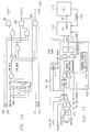
- FIGURE 7 is a block diagram of a cloak acquisition system similar to Figure 1, with a control register to control low power modes with hardware controlled deep sleep wakeup.
- Today's data processing systems can have very low power modes. When devices are powered down, most if not all clocks are turned “OFF" within the system clock acquisition subsystem. Generally the power down modes are invoked by software sequences executed within the microprocessor or micro controller devices within these systems.
- Clock sources include crystal oscillators or phase locked loops (PLLs) which have long startup times. These start up times extend the interrupt latency when a device "wakes up" from a deep sleep low power mode.
- PLLs phase locked loops
- a reference frequency such as an oscillator
- an interlocked clock multiplexer clock switch mechanism is included in the system.
- An ICM provides the ability to switch to the PLL reference prior to deep sleep or immediately after wakeup from a deep sleep, even when the reference clock and the PLL output have similar frequencies.
- FIGURE 7 represents a system level block diagram of a system featuring a capability to automatically select oscillator 710 as the clock source prior to operation after wakeup from deep sleep with circuitry to restart and automatically select PLL 720 as the system clock source after wakeup when PLL 710 has stabilized.
- ICM 100 acquires a CLKOUT signal 102 from either of clock source signals 104 or 106 in response to SEL_A signal 108 which is generated by clock selection logic 740.
- clock A signal 104 and clock B signal 106 are not limited to single sources.
- the clock selection and power down modes are specified with a three bit (LPM_M[2:0]) low power mode selection code field 730a in clock control register 730.
- the three bit code is used as outlined in Table 1.
- Wakeup logic 750 generates an oscillator enable signal 751 in response to various wakeup events which is connected to clock selection logic 740.
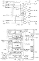
- FIGURE 8 is a circuit diagram of power down selection logic 740 of Figure 7, with hardware control for re-enabling the phase locked loop.
- Oscillator OK signal(OSCOK) 752 is produced by oscillator 710 when the oscillator is operational.
- PLL OK signal 753 is produced by PLL 720 when the PLL is locked in to a reference signal and is operational.
- Gates 761-764 form control signals PLL_OFF, OSC_OFF, and SEL_A in order to produce the clock selection sequences contained in Table 1.
- CLK_OK signal 765 is asserted when the selected clock source is operational.
- FIGURE 9 is a block diagram of a clock acquisition system similar to Figure 7, with a control register to control low power modes, with software controlled deep sleep wakeup.
- This embodiment of the present invention is a system featuring an automatic switch from PLL 820 to oscillator 710 as the clock source for use after wakeup from deep sleep and software directed selection of PLL 820 as the system clock source after wakeup when PLL 820 has stabilized.
- This system is similar to that shown in Figure 7 but does not support as many power down modes.
- the hardware circuitry establishes the oscillator as the system clock source during a deep sleep powerdown in response to OSCOFF signal 862 being asserted.
- the clock selection and powerdown modes are specified with a two bit (LPM_M[1:0]) low power mode selection code in clock control register 830.
- the two bit code is used as outlined in Table 2.
- HW Clock Control For Deep Sleep Wake Up Definition LPM_M[1:0] Description 00 Osc. "ON”, PLL “OFF”, Osc. is Clock Source, No Powerdown 01 Osc. “ON”, PLL “OFF”, Osc. is Clock Source, Osc. "OFF” when OSCEN ⁇ FALSE 10 Osc. "ON”, PLL “ON”, PLL is Clock Source, No Powerdown 11 Osc.
- FIGURE 10 is a circuit diagram of the power down selection logic of Figure 9, with software control for re-enabling the phase locked loop.
- Oscillator OK signal 752 is produced by oscillator 710 when the oscillator is operational.
- Gates 861-863 form control signals PLLOFF, OSCOFF, and SEL_A in order to produce the clock selection sequences contained in Table 2.
- CLKOK signal 865 is asserted when oscillator 710 is operational.
- FIGURE 11 is a block diagram of a clock acquisition system using a triple throw interlocked clock multiplexer.
- Oscillator 1110 generates CLKA signal 104, while divider 1111 divides the frequency of CLKA by two and forms CLKB signal 106.
- PLL is locked to oscillator 1110 and forms CLKC signal 1107, which has a frequency which differs from CLKA by a factor of 1, 2, 3, 4, 5, or 9 as determined by divider 1121.
- ICM 1100 acquires a CLKOUT signal 102 which is provided to microprocessor 1170 in response to control signals 1108.
- FIGURE 12 is a circuit diagram of the triple throw interlocked clock multiplexer of FIGURE 11, according to the present invention.
- ICM 1100 is another embodiment of an interlocked clock multiplexer which is similar to ICM 100, but switches between three clock source signals CLKA 104, CLKB 106 and CLKC 1107 in response to select signals SEL0 1108a and SEL1 1108b to acquire a clean, substantially glitch free output clock signal 102 which has selected clock characteristics.
- CLKC signal 1107 is typically generated by PLL 1120.
- the PLL may also provide a "PLL_OK" signal 1108e which indicates that the PLL has locked and is generating a good CLKC signal.
- ICM 1100 is controlled by control signals SEL0 and SEL1, whose truth table is listed in Table 3.
- the circuitry of ICM 1100 is designed so that no more than one clock source can be selected at a time.
- the CLKA synchronizer 310, CLKB synchronizer 312 and CLKC synchronizer 1213 are interlocked to form a cross-coupled switch. If CLKA is selected CLKB or CLKC can not be selected until CLKA is deselected. The same holds true for other combinations of CLKA, CLKB, & CLKC.
- the 2-stage synchronizer for each clock source ensures that there will be no glitches during a switch by creating a wait state which is approximately two cycles after "breaking" a prior selection and before “making” a new selection, as described with reference to FIGUREs 4 and 5.
- PLL_off signal PLL_OFF and all clocks off signal ALL_OFF may be formed by circuitry such as illustrated in FIGUREs 8 or 10 using a control register such as control register 730 or 930.
- a low power mode is generally not entered until processor 1170 executes an IDLE instruction or writes a bit to a control register to indicate that a low power mode is to be entered.
- oscillator enable signal 751 is de-asserted until a wakeup event occurs.
- clock output signal 102 is switched from CLKC to CLKA or CLKB, depending on the value of SEL0, after appropriate synchronization as described previously according to the present invention. PLL 1120 can then be disabled. When PLL_OFF is de-asserted again, clockout signal 102 will continue to be supplied by CLKA/CLKB until PLL_OK goes HIGH, indicating that CLKC is stable. At this time, CLKC will be acquired by ICM 1100 to form clock out signal 102 after appropriate synchronization.
- ALL_OFF is asserted and CLKA or CLKB is currently selected, all clocks will be deselected and CLKOUT will go LOW after appropriate synchronization. At this time, all clock sources can then be shut “OFF”. When ALL_OFF is de-asserted again, either CLKA or CLKB will be selected, depending on the value of SEL0, after appropriate synchronization.
- Another aspect of the present invention is that when ALL_OFF is asserted and CLKC is currently selected, CLKOUT will be switched from CLKC to CLKA or CLKB, depending on the value of SEL0, as described above. Once CLKOUT has been switched to CLKA or CLKB, the current state will be captured by the RS latches 1261 or 1262 (WAS_A or WAS_B) and then all clocks will be deselected and CLKOUT will go LOW after synchronization.
- ALL_OFF is de-asserted again, CLKA or CLKB will be selected depending on the values latched in RS latches 1261-1262. CLKOUT will continue to be supplied by CLKA/CLKB until PLL_OK goes HIGH indicating CLKC is stable. Then CLKOUT will be switched back to CLKC after synchronization.
- An advantage of this clock switching sequence is that processor 1170 can quickly begin operation after a wakeup event using CLKA or CLKB, and then automatically switch to CLKC when PLL 1120 is stable.
- FIGURE 13 is a circuit diagram of an optional circuit which may be connected to the interlocked clock multiplexer of FIGUREs 3 or 12 for forcing at least one clock source to be active after power is restored.
- one or more synchronizers 310, 312, or 1213 may be set into an anomalous state during application of power to the clock acquisition subsystem.
- the circuit of FIGURE 13 detects if more than one clock is selected with gate 1360 and detects if no clocks are selected with gate 1361. If signal ALL_OFF is not asserted, then gate 1362 will enable gate 1363 to form an enable oscillator signal regardless of the state of signal OSC_OFF and will enable gate 1364 to form a PLL enable signal. By turning “ON" the oscillator and PLL, clock signals will be applied to synchronizers 310, 312, and 1213 which will cause an anomalous state to be eliminated.
- circuits of the present invention have many advantageous uses in data processing systems. Any one of a large number of clock sources can be selected to optimize the speed of processing for a specific situation, and then be changed to a different clock source for a different optimization under control of a program operating in the data processing system.
- Another advantage is that various clock switching sequences can be performed when entering and leaving a low power mode either automatically or under software control.
- Embodiments of the present invention have been described which have a double throw ICM for selecting between two clock source signals and a triple throw ICM for selecting from three clock source signals, where each clock source signal may be derived from a number of clock sources.
- Other embodiments may be constructed in a similar manner having an ICM with more than three clock signal inputs.
- connection means electrically connected, including where additional elements may be in the electrical connection path.
Landscapes
- Engineering & Computer Science (AREA)
- Theoretical Computer Science (AREA)
- Physics & Mathematics (AREA)
- General Engineering & Computer Science (AREA)
- General Physics & Mathematics (AREA)
- Stabilization Of Oscillater, Synchronisation, Frequency Synthesizers (AREA)
- Power Sources (AREA)
- Microcomputers (AREA)
Applications Claiming Priority (2)
| Application Number | Priority Date | Filing Date | Title |
|---|---|---|---|
| US743480 | 1996-11-04 | ||
| US08/743,480 US5903746A (en) | 1996-11-04 | 1996-11-04 | Apparatus and method for automatically sequencing clocks in a data processing system when entering or leaving a low power state |
Publications (3)
| Publication Number | Publication Date |
|---|---|
| EP0840195A2 true EP0840195A2 (de) | 1998-05-06 |
| EP0840195A3 EP0840195A3 (de) | 1998-05-13 |
| EP0840195B1 EP0840195B1 (de) | 2004-01-28 |
Family
ID=24988942
Family Applications (1)
| Application Number | Title | Priority Date | Filing Date |
|---|---|---|---|
| EP97308829A Expired - Lifetime EP0840195B1 (de) | 1996-11-04 | 1997-11-04 | Anordnung und Verfahren zur Taktsequenzierung in einem Datenverarbeitungssystem |
Country Status (4)
| Country | Link |
|---|---|
| US (1) | US5903746A (de) |
| EP (1) | EP0840195B1 (de) |
| JP (1) | JPH10161767A (de) |
| DE (1) | DE69727355T2 (de) |
Cited By (2)
| Publication number | Priority date | Publication date | Assignee | Title |
|---|---|---|---|---|
| EP1544717A2 (de) * | 2003-12-17 | 2005-06-22 | Via Technologies, Inc. | Frequenz- und Spannungssteuervorrichtung zur Leistungsverwaltung eines Mikroprozessors |
| WO2006053202A1 (en) * | 2004-11-12 | 2006-05-18 | U-Nav Microelectronics Corporation | Glitchless clock multiplexer controlled by an asynchronous select signal |
Families Citing this family (33)
| Publication number | Priority date | Publication date | Assignee | Title |
|---|---|---|---|---|
| JPH11143571A (ja) * | 1997-11-05 | 1999-05-28 | Mitsubishi Electric Corp | データ処理装置 |
| US6237106B1 (en) * | 1997-11-06 | 2001-05-22 | Canon Kabushiki Kaisha | Communication apparatus and method, and program in computer readable medium |
| US6070248A (en) * | 1997-12-12 | 2000-05-30 | Advanced Micro Devices, Inc. | Generation of a stable reference clock frequency from a base clock frequency that may vary depending on source |
| US6275546B1 (en) * | 1998-06-30 | 2001-08-14 | Hewlett-Packard Company | Glitchless clock switch circuit |
| US6323715B1 (en) | 1999-12-30 | 2001-11-27 | Koninklijke Philips Electronics N.V. (Kpeuv) | Method and apparatus for selecting a clock signal without producing a glitch |
| US6578155B1 (en) * | 2000-03-16 | 2003-06-10 | International Business Machines Corporation | Data processing system with adjustable clocks for partitioned synchronous interfaces |
| KR20020014534A (ko) * | 2000-08-18 | 2002-02-25 | 박종섭 | 저전력 오디오 프로세서 |
| US6467042B1 (en) * | 2000-12-27 | 2002-10-15 | Cypress Semiconductor Corporation | Method and/or apparatus for lowering power consumption in a peripheral device |
| US7039146B2 (en) * | 2001-01-16 | 2006-05-02 | Advanced Micro Devices, Inc. | Method and interface for glitch-free clock switching |
| US7912989B2 (en) * | 2001-05-16 | 2011-03-22 | Ricoh Company, Ltd. | Network interface for decreasing power consumption |
| US6968219B2 (en) * | 2001-08-15 | 2005-11-22 | Qualcomm, Incorporated | Method for reducing power consumption in bluetooth and CDMA modes of operation |
| US7210054B2 (en) * | 2002-06-25 | 2007-04-24 | Intel Corporation | Maintaining processor execution during frequency transitioning |
| JP3542351B2 (ja) * | 2002-11-18 | 2004-07-14 | 沖電気工業株式会社 | クロック切り替え回路 |
| US20040107375A1 (en) * | 2002-12-02 | 2004-06-03 | Edward Anglada | System and method for switching clock sources |
| US7080271B2 (en) * | 2003-02-14 | 2006-07-18 | Intel Corporation | Non main CPU/OS based operational environment |
| JP4152795B2 (ja) * | 2003-04-03 | 2008-09-17 | 株式会社ルネサステクノロジ | マイクロコントローラ |
| JP3958720B2 (ja) * | 2003-07-22 | 2007-08-15 | 沖電気工業株式会社 | クロック制御回路とクロック制御方法 |
| US7131024B1 (en) * | 2003-09-24 | 2006-10-31 | Altera Corporation | Multiple transmit data rates in programmable logic device serial interface |
| CN100470656C (zh) | 2003-10-31 | 2009-03-18 | 宇田控股有限公司 | 摆动时钟信号的产生方法和产生装置 |
| US8385985B2 (en) * | 2003-11-25 | 2013-02-26 | Qualcomm Incorporated | Method for reducing power consumption in a multi-mode device |
| US7281149B2 (en) * | 2004-02-24 | 2007-10-09 | Hewlett-Packard Development Company, L.P. | Systems and methods for transitioning a CPU from idle to active |
| US7181188B2 (en) * | 2004-03-23 | 2007-02-20 | Freescale Semiconductor, Inc. | Method and apparatus for entering a low power mode |
| US7496774B2 (en) * | 2004-06-04 | 2009-02-24 | Broadcom Corporation | Method and system for generating clocks for standby mode operation in a mobile communication device |
| FR2874766A1 (fr) * | 2004-09-02 | 2006-03-03 | St Microelectronics Sa | Procede de configuration du systeme d'horloge d'un microcontroleur |
| JP2006224520A (ja) * | 2005-02-18 | 2006-08-31 | Seiko Epson Corp | 印刷装置のコントローラ |
| US7882384B2 (en) * | 2006-08-31 | 2011-02-01 | National Semiconductor Corporation | Setting and minimizing a derived clock frequency based on an input time interval |
| US7929574B2 (en) * | 2007-11-30 | 2011-04-19 | Alcatel Lucent | Advanced clock distribution mechanism for circuit emulation applications |
| US8054144B2 (en) | 2008-07-02 | 2011-11-08 | Atmel Corporation | Mode switching RC network |
| JP6389188B2 (ja) * | 2012-12-13 | 2018-09-12 | コーヒレント・ロジックス・インコーポレーテッド | 同期型デジタルシステムにおけるチップ間通信のための多重周波数クロックスキュー制御 |
| US9383805B2 (en) | 2013-03-12 | 2016-07-05 | Atmel Corporation | Generating clock on demand |
| JP2015176214A (ja) * | 2014-03-13 | 2015-10-05 | 株式会社東芝 | 通信装置 |
| US12135599B1 (en) | 2023-05-31 | 2024-11-05 | International Business Machines Corporation | Dynamic computing environment channel enablement |
| CN121525628A (zh) * | 2026-01-16 | 2026-02-13 | 湖南进芯电子科技有限公司 | 一种低功耗多核soc |
Family Cites Families (28)
| Publication number | Priority date | Publication date | Assignee | Title |
|---|---|---|---|---|
| US3453601A (en) * | 1966-10-18 | 1969-07-01 | Philco Ford Corp | Two speed arithmetic calculator |
| US3623017A (en) * | 1969-10-22 | 1971-11-23 | Sperry Rand Corp | Dual clocking arrangement for a digital computer |
| NL7207216A (de) * | 1972-05-27 | 1973-11-29 | ||
| GB1561961A (en) * | 1977-04-20 | 1980-03-05 | Int Computers Ltd | Data processing units |
| JPS54144152A (en) * | 1978-04-28 | 1979-11-10 | Sharp Corp | Integrated circuit device |
| US4279020A (en) * | 1978-08-18 | 1981-07-14 | Bell Telephone Laboratories, Incorporated | Power supply circuit for a data processor |
| US4381552A (en) * | 1978-12-08 | 1983-04-26 | Motorola Inc. | Stanby mode controller utilizing microprocessor |
| US4293927A (en) * | 1979-12-12 | 1981-10-06 | Casio Computer Co., Ltd. | Power consumption control system for electronic digital data processing devices |
| US4409665A (en) * | 1979-12-26 | 1983-10-11 | Texas Instruments Incorporated | Turn-off-processor between keystrokes |
| JPS58127262A (ja) * | 1982-01-25 | 1983-07-29 | Toshiba Corp | マイクロコンピユ−タ |
| US4698748A (en) * | 1983-10-07 | 1987-10-06 | Essex Group, Inc. | Power-conserving control system for turning-off the power and the clocking for data transactions upon certain system inactivity |
| US4819164A (en) * | 1983-12-12 | 1989-04-04 | Texas Instruments Incorporated | Variable frequency microprocessor clock generator |
| JPS61147324A (ja) * | 1984-12-20 | 1986-07-05 | Matsushita Electric Ind Co Ltd | クロツク制御回路 |
| US4821229A (en) * | 1985-12-12 | 1989-04-11 | Zenith Electronics Corporation | Dual operating speed switchover arrangement for CPU |
| US4851987A (en) * | 1986-01-17 | 1989-07-25 | International Business Machines Corporation | System for reducing processor power consumption by stopping processor clock supply if a desired event does not occur |
| US4814591A (en) * | 1987-04-13 | 1989-03-21 | Kabushiki Kaisha Toshiba | Portable medium |
| DK174975B1 (da) * | 1988-05-06 | 2004-04-05 | Toppan Printing Co Ltd | Integreret kredsløbskort |
| US4980836A (en) * | 1988-10-14 | 1990-12-25 | Compaq Computer Corporation | Apparatus for reducing computer system power consumption |
| EP0363567B1 (de) * | 1988-10-14 | 1994-11-30 | International Business Machines Corporation | Rechner mit unterbrechungsgesteuerter Taktgeschwindigkeit und Verfahren für seinen Betrieb |
| US5123107A (en) * | 1989-06-20 | 1992-06-16 | Mensch Jr William D | Topography of CMOS microcomputer integrated circuit chip including core processor and memory, priority, and I/O interface circuitry coupled thereto |
| US5167024A (en) * | 1989-09-08 | 1992-11-24 | Apple Computer, Inc. | Power management for a laptop computer with slow and sleep modes |
| US5218704A (en) * | 1989-10-30 | 1993-06-08 | Texas Instruments | Real-time power conservation for portable computers |
| WO1996025796A1 (en) * | 1995-02-17 | 1996-08-22 | Intel Corporation | Power dissipation control system for vlsi chips |
| US5592173A (en) * | 1994-07-18 | 1997-01-07 | Trimble Navigation, Ltd | GPS receiver having a low power standby mode |
| US5479648A (en) * | 1994-08-30 | 1995-12-26 | Stratus Computer, Inc. | Method and apparatus for switching clock signals in a fault-tolerant computer system |
| US5586308A (en) * | 1994-10-19 | 1996-12-17 | Advanced Micro Devices, Inc. | Clock control unit responsive to a power management state for clocking multiple clocked circuits connected thereto |
| US5550489A (en) * | 1995-09-29 | 1996-08-27 | Quantum Corporation | Secondary clock source for low power, fast response clocking |
| US5790609A (en) * | 1996-11-04 | 1998-08-04 | Texas Instruments Incorporated | Apparatus for cleanly switching between various clock sources in a data processing system |
-
1996
- 1996-11-04 US US08/743,480 patent/US5903746A/en not_active Expired - Lifetime
-
1997
- 1997-11-04 EP EP97308829A patent/EP0840195B1/de not_active Expired - Lifetime
- 1997-11-04 JP JP9302128A patent/JPH10161767A/ja active Pending
- 1997-11-04 DE DE69727355T patent/DE69727355T2/de not_active Expired - Lifetime
Cited By (3)
| Publication number | Priority date | Publication date | Assignee | Title |
|---|---|---|---|---|
| EP1544717A2 (de) * | 2003-12-17 | 2005-06-22 | Via Technologies, Inc. | Frequenz- und Spannungssteuervorrichtung zur Leistungsverwaltung eines Mikroprozessors |
| WO2006053202A1 (en) * | 2004-11-12 | 2006-05-18 | U-Nav Microelectronics Corporation | Glitchless clock multiplexer controlled by an asynchronous select signal |
| US8350600B2 (en) | 2004-11-12 | 2013-01-08 | Qualcomm Incorporated | Glitchless clock multiplexer controlled by an asynchronous select signal |
Also Published As
| Publication number | Publication date |
|---|---|
| DE69727355T2 (de) | 2004-11-11 |
| EP0840195A3 (de) | 1998-05-13 |
| JPH10161767A (ja) | 1998-06-19 |
| DE69727355D1 (de) | 2004-03-04 |
| US5903746A (en) | 1999-05-11 |
| EP0840195B1 (de) | 2004-01-28 |
Similar Documents
| Publication | Publication Date | Title |
|---|---|---|
| EP0840195B1 (de) | Anordnung und Verfahren zur Taktsequenzierung in einem Datenverarbeitungssystem | |
| US5790609A (en) | Apparatus for cleanly switching between various clock sources in a data processing system | |
| EP1451666B1 (de) | Störungsfreie taktauswahlschaltung | |
| KR100379766B1 (ko) | 순간클럭주파수시프트기능을구비한pll시스템클럭발생기 | |
| US5550489A (en) | Secondary clock source for low power, fast response clocking | |
| KR100358889B1 (ko) | 휴대용개인정보기기에적합한집적프로세서시스템 | |
| US6016071A (en) | Internal source clock generation circuit for use with power management scheme | |
| US5315181A (en) | Circuit for synchronous, glitch-free clock switching | |
| US7594126B2 (en) | Processor system and method for reducing power consumption in idle mode | |
| US6563349B2 (en) | Multiplexor generating a glitch free output when selecting from multiple clock signals | |
| KR100385155B1 (ko) | 외부핀신호를다중화하는장치를포함하는집적프로세서 | |
| KR960015134A (ko) | 전력 관리상태에 응답하여 다중 클럭된 회로를 클럭하는 클럭 제어기 | |
| US5915107A (en) | Cross clock domain clocking for a system using two clock frequencies where one frequency is fractional multiple of the other | |
| US10969854B2 (en) | Semiconductor device including clock management unit for outputing clock and acknowledgement signals to an intellectual property block | |
| JP2011180736A (ja) | クロック制御信号生成回路、クロックセレクタ、及び情報処理装置 | |
| TWI446720B (zh) | 積體電路時脈管理技術 | |
| KR19990014219A (ko) | 클록 생성 방법 및 장치 | |
| JPH11312026A (ja) | クロック信号切替方法およびクロック信号切替システム | |
| US6675249B2 (en) | Information processing equipment and information processing system | |
| US20030145244A1 (en) | Glitchless clock selection circuit | |
| US5568100A (en) | Synchronous power down clock oscillator device | |
| US7243244B2 (en) | Microprocessor and operation mode switching method for the microprocessor | |
| US6157233A (en) | Always-deterministic phase-locked loop | |
| WO1999063665A1 (en) | A tunable digital oscillator circuit and method for producing clock signals of different frequencies | |
| CN119311106A (zh) | 一种低功耗mcu的无时钟唤醒电路及方法 |
Legal Events
| Date | Code | Title | Description |
|---|---|---|---|
| PUAI | Public reference made under article 153(3) epc to a published international application that has entered the european phase |
Free format text: ORIGINAL CODE: 0009012 |
|
| PUAL | Search report despatched |
Free format text: ORIGINAL CODE: 0009013 |
|
| AK | Designated contracting states |
Kind code of ref document: A2 Designated state(s): DE FR GB IT NL |
|
| AX | Request for extension of the european patent |
Free format text: AL;LT;LV;MK;RO;SI |
|
| AK | Designated contracting states |
Kind code of ref document: A3 Designated state(s): AT BE CH DE DK ES FI FR GB GR IE IT LI LU MC NL PT SE |
|
| AX | Request for extension of the european patent |
Free format text: AL;LT;LV;MK;RO;SI |
|
| 17P | Request for examination filed |
Effective date: 19980918 |
|
| AKX | Designation fees paid |
Free format text: DE FR GB IT NL |
|
| RBV | Designated contracting states (corrected) |
Designated state(s): DE FR GB IT NL |
|
| 17Q | First examination report despatched |
Effective date: 20021128 |
|
| GRAP | Despatch of communication of intention to grant a patent |
Free format text: ORIGINAL CODE: EPIDOSNIGR1 |
|
| GRAS | Grant fee paid |
Free format text: ORIGINAL CODE: EPIDOSNIGR3 |
|
| GRAA | (expected) grant |
Free format text: ORIGINAL CODE: 0009210 |
|
| AK | Designated contracting states |
Kind code of ref document: B1 Designated state(s): DE FR GB IT NL |
|
| PG25 | Lapsed in a contracting state [announced via postgrant information from national office to epo] |
Ref country code: NL Free format text: LAPSE BECAUSE OF FAILURE TO SUBMIT A TRANSLATION OF THE DESCRIPTION OR TO PAY THE FEE WITHIN THE PRESCRIBED TIME-LIMIT Effective date: 20040128 Ref country code: IT Free format text: LAPSE BECAUSE OF FAILURE TO SUBMIT A TRANSLATION OF THE DESCRIPTION OR TO PAY THE FEE WITHIN THE PRESCRIBED TIME-LIMIT;WARNING: LAPSES OF ITALIAN PATENTS WITH EFFECTIVE DATE BEFORE 2007 MAY HAVE OCCURRED AT ANY TIME BEFORE 2007. THE CORRECT EFFECTIVE DATE MAY BE DIFFERENT FROM THE ONE RECORDED. Effective date: 20040128 |
|
| REG | Reference to a national code |
Ref country code: GB Ref legal event code: FG4D |
|
| REF | Corresponds to: |
Ref document number: 69727355 Country of ref document: DE Date of ref document: 20040304 Kind code of ref document: P |
|
| NLV1 | Nl: lapsed or annulled due to failure to fulfill the requirements of art. 29p and 29m of the patents act | ||
| ET | Fr: translation filed | ||
| PLBE | No opposition filed within time limit |
Free format text: ORIGINAL CODE: 0009261 |
|
| STAA | Information on the status of an ep patent application or granted ep patent |
Free format text: STATUS: NO OPPOSITION FILED WITHIN TIME LIMIT |
|
| 26N | No opposition filed |
Effective date: 20041029 |
|
| PGFP | Annual fee paid to national office [announced via postgrant information from national office to epo] |
Ref country code: FR Payment date: 20121113 Year of fee payment: 16 Ref country code: DE Payment date: 20121130 Year of fee payment: 16 |
|
| PGFP | Annual fee paid to national office [announced via postgrant information from national office to epo] |
Ref country code: GB Payment date: 20121025 Year of fee payment: 16 |
|
| GBPC | Gb: european patent ceased through non-payment of renewal fee |
Effective date: 20131104 |
|
| REG | Reference to a national code |
Ref country code: FR Ref legal event code: ST Effective date: 20140731 |
|
| REG | Reference to a national code |
Ref country code: DE Ref legal event code: R119 Ref document number: 69727355 Country of ref document: DE Effective date: 20140603 |
|
| PG25 | Lapsed in a contracting state [announced via postgrant information from national office to epo] |
Ref country code: DE Free format text: LAPSE BECAUSE OF NON-PAYMENT OF DUE FEES Effective date: 20140603 |
|
| PG25 | Lapsed in a contracting state [announced via postgrant information from national office to epo] |
Ref country code: GB Free format text: LAPSE BECAUSE OF NON-PAYMENT OF DUE FEES Effective date: 20131104 Ref country code: FR Free format text: LAPSE BECAUSE OF NON-PAYMENT OF DUE FEES Effective date: 20131202 |