EP0840198A2 - Verfahren und Vorrichtung zur Erweiterung der Speicherkapazität eines Rechners - Google Patents
Verfahren und Vorrichtung zur Erweiterung der Speicherkapazität eines Rechners Download PDFInfo
- Publication number
- EP0840198A2 EP0840198A2 EP97308436A EP97308436A EP0840198A2 EP 0840198 A2 EP0840198 A2 EP 0840198A2 EP 97308436 A EP97308436 A EP 97308436A EP 97308436 A EP97308436 A EP 97308436A EP 0840198 A2 EP0840198 A2 EP 0840198A2
- Authority
- EP
- European Patent Office
- Prior art keywords
- memory
- module
- memory module
- extends beyond
- recited
- Prior art date
- Legal status (The legal status is an assumption and is not a legal conclusion. Google has not performed a legal analysis and makes no representation as to the accuracy of the status listed.)
- Withdrawn
Links
Images

Classifications
-
- G—PHYSICS
- G06—COMPUTING OR CALCULATING; COUNTING
- G06F—ELECTRIC DIGITAL DATA PROCESSING
- G06F1/00—Details not covered by groups G06F3/00 - G06F13/00 and G06F21/00
- G06F1/16—Constructional details or arrangements
- G06F1/18—Packaging or power distribution
- G06F1/183—Internal mounting support structures, e.g. for supporting printed circuit boards
- G06F1/185—Mounting of expansion boards
-
- G—PHYSICS
- G06—COMPUTING OR CALCULATING; COUNTING
- G06F—ELECTRIC DIGITAL DATA PROCESSING
- G06F1/00—Details not covered by groups G06F3/00 - G06F13/00 and G06F21/00
- G06F1/16—Constructional details or arrangements
- G06F1/18—Packaging or power distribution
- G06F1/183—Internal mounting support structures, e.g. for supporting printed circuit boards
- G06F1/184—Mounting of motherboards
-
- G—PHYSICS
- G06—COMPUTING OR CALCULATING; COUNTING
- G06F—ELECTRIC DIGITAL DATA PROCESSING
- G06F1/00—Details not covered by groups G06F3/00 - G06F13/00 and G06F21/00
- G06F1/16—Constructional details or arrangements
- G06F1/18—Packaging or power distribution
- G06F1/183—Internal mounting support structures, e.g. for supporting printed circuit boards
- G06F1/185—Mounting of expansion boards
- G06F1/186—Securing of expansion boards in correspondence to slots provided at the computer enclosure
-
- H—ELECTRICITY
- H05—ELECTRIC TECHNIQUES NOT OTHERWISE PROVIDED FOR
- H05K—PRINTED CIRCUITS; CASINGS OR CONSTRUCTIONAL DETAILS OF ELECTRIC APPARATUS; MANUFACTURE OF ASSEMBLAGES OF ELECTRICAL COMPONENTS
- H05K1/00—Printed circuits
- H05K1/18—Printed circuits structurally associated with non-printed electric components
- H05K1/181—Printed circuits structurally associated with non-printed electric components associated with surface mounted components
-
- H—ELECTRICITY
- H05—ELECTRIC TECHNIQUES NOT OTHERWISE PROVIDED FOR
- H05K—PRINTED CIRCUITS; CASINGS OR CONSTRUCTIONAL DETAILS OF ELECTRIC APPARATUS; MANUFACTURE OF ASSEMBLAGES OF ELECTRICAL COMPONENTS
- H05K1/00—Printed circuits
- H05K1/02—Details
- H05K1/0284—Details of three-dimensional rigid printed circuit boards
-
- H—ELECTRICITY
- H05—ELECTRIC TECHNIQUES NOT OTHERWISE PROVIDED FOR
- H05K—PRINTED CIRCUITS; CASINGS OR CONSTRUCTIONAL DETAILS OF ELECTRIC APPARATUS; MANUFACTURE OF ASSEMBLAGES OF ELECTRICAL COMPONENTS
- H05K1/00—Printed circuits
- H05K1/02—Details
- H05K1/14—Structural association of two or more printed circuits
- H05K1/141—One or more single auxiliary printed circuits mounted on a main printed circuit, e.g. modules, adapters
-
- H—ELECTRICITY
- H05—ELECTRIC TECHNIQUES NOT OTHERWISE PROVIDED FOR
- H05K—PRINTED CIRCUITS; CASINGS OR CONSTRUCTIONAL DETAILS OF ELECTRIC APPARATUS; MANUFACTURE OF ASSEMBLAGES OF ELECTRICAL COMPONENTS
- H05K2201/00—Indexing scheme relating to printed circuits covered by H05K1/00
- H05K2201/09—Shape and layout
- H05K2201/09009—Substrate related
- H05K2201/09027—Non-rectangular flat PCB, e.g. circular
-
- H—ELECTRICITY
- H05—ELECTRIC TECHNIQUES NOT OTHERWISE PROVIDED FOR
- H05K—PRINTED CIRCUITS; CASINGS OR CONSTRUCTIONAL DETAILS OF ELECTRIC APPARATUS; MANUFACTURE OF ASSEMBLAGES OF ELECTRICAL COMPONENTS
- H05K2201/00—Indexing scheme relating to printed circuits covered by H05K1/00
- H05K2201/10—Details of components or other objects attached to or integrated in a printed circuit board
- H05K2201/10007—Types of components
- H05K2201/10159—Memory
-
- H—ELECTRICITY
- H05—ELECTRIC TECHNIQUES NOT OTHERWISE PROVIDED FOR
- H05K—PRINTED CIRCUITS; CASINGS OR CONSTRUCTIONAL DETAILS OF ELECTRIC APPARATUS; MANUFACTURE OF ASSEMBLAGES OF ELECTRICAL COMPONENTS
- H05K3/00—Apparatus or processes for manufacturing printed circuits
- H05K3/36—Assembling printed circuits with other printed circuits
- H05K3/366—Assembling printed circuits with other printed circuits substantially perpendicularly to each other
-
- Y—GENERAL TAGGING OF NEW TECHNOLOGICAL DEVELOPMENTS; GENERAL TAGGING OF CROSS-SECTIONAL TECHNOLOGIES SPANNING OVER SEVERAL SECTIONS OF THE IPC; TECHNICAL SUBJECTS COVERED BY FORMER USPC CROSS-REFERENCE ART COLLECTIONS [XRACs] AND DIGESTS
- Y02—TECHNOLOGIES OR APPLICATIONS FOR MITIGATION OR ADAPTATION AGAINST CLIMATE CHANGE
- Y02P—CLIMATE CHANGE MITIGATION TECHNOLOGIES IN THE PRODUCTION OR PROCESSING OF GOODS
- Y02P70/00—Climate change mitigation technologies in the production process for final industrial or consumer products
- Y02P70/50—Manufacturing or production processes characterised by the final manufactured product
Definitions
- the present invention relates generally to computer memory modules. More particularly, the present invention relates to memory module form factors that maximize memory density.
- DRAM Dynamic Random Access Memory
- DRAM packaging has been evolving. Several years ago, memory was pin throughhole packaged. Today, with the common use of surface mount technology, small outline integrated circuit (SOIC), thin small outline package (TSOP), and like configurations are most common.
- SOIC small outline integrated circuit
- TSOP thin small outline package
- Memory modules serve at least two functions. One function is to make DRAM's compatible with the system bus organization, that is, reflective of the system designers' desire to match the processor bus size. Second, memory modules allow for easy upgrades.
- SIMMs are in four basic types: one-byte modules (30-pin single-in-line memory modules (SIMMS), four-byte modules (72- pin SIMMs or 72-pin small outline, dual in-line memory modules (SODIMMs), eight-byte modules (168-pin DIMMs), and custom modules (e.g., HP 9000 workstation memory).
- SIMMs were first developed by Wang in the mid-1970's in conjunction with Molex, the connector supplier for Wang's "office assistant" word processor. While SIMMs have, generally, 30 or 72 contacts that are the same on both sides of the "card," DIMMs have two (dual) rows of contacts, one row on each side of the card.
- a computer can retrieve information from DIMMs 64 bits at a time instead of the 32 or 16 - bit transfers usual with SIMMs.
- SODIMMs have 72-pins, making them relatively compact and thus particularly well suited for memory expansion in portables.
- the present invention overcomes the shortcomings and deficiencies mentioned above by providing a computer system including a memory module formed of a first portion having a first side that directly connects to a mount in the system, which first side is of a first length; and which memory module is also formed of a second portion having a second side, which second side is of a second length, the second length being greater than the first length.
- the second side extends beyond the first side in two directions, thereby forming a "T-shape".
- the second side defines a nonlinear element, such as an arc.
- the present invention also provides a method for increasing memory capacity in a system, which method includes the steps of providing a module with an area that extends beyond its connector footprint, mounting memory elements on the module so that at least a portion of memory is disposed in the area that extends beyond the module's connector footprint, and connecting the memory module with memory mounted thereon to the system.
- an object of the present invention is to provide simple methods and apparatus for maximizing DRAM density within the space constraints of existing computer systems.
- Another object of the present invention is to introduce new forms of memory modules, so there is greater choice in how memory can be disposed in systems which use the memory.
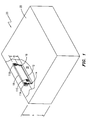
- FIG. 1 there is shown a preferred embodiment of the present invention in the form of a memory module 10.
- Memory module 10 is shown in FIG. 1 to be mounted in a slot 12, and held by retaining arms 14, 16, on a board 18 in computer system 20.
- Computer system 20 in FIG. 1 is depicted as a housing 22 that is partially cut away to show module 10.
- housing 22 would likely be formed in parts to allow ready access to internal components; those parts are not depicted.
- computer system 20 would also likely comprise a processor, power supply, hard drive, and other conventional components; those components are not depicted either.
- the instant invention resides in the form of memory modules; that being so, aspects of system 20 that do not directly affect, or are not directly involved in the operation of the module 10, which aspects would not help clarify or explain the instant invention, are not depicted herein.
- Conventional computer systems generally include slots and retaining arms for the mounting of memory modules.
- a memory module according to the teachings of the present invention should be understood as being readily insertable into and retainable by such "prior art" slots and arms.
- the module 10 readily fits within the confines of the housing 22. More specifically, in FIG. 1 the housing 22 may be seen to have a height "h.”
- the memory module 10 has a height "m,” taking into account its elevated status in the slot 12, with height "m” clearly being less than "h.”
- height "h" In the evaluation of computer systems, especially insofar as that evolution has led to development of notebook computers, which have very small height "h", there is less and less "real estate” or space for conventional memory modules for memory elements.
- conventional memory modules are rectangular, with the length of the module base being fixed by the size of conventional slots into which the modules are inserted.
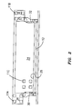
- memory module 10 has an increased amount of real estate relative to prior art memory modules, without an overly limiting increase in height, by comprising a first portion 24 and a second portion 26.
- the first portion is like conventional memory module, insofar as it is rectangular, with a base 28 substantially equal in length to the slot 12 in which it is inserted.
- the second portion 26 projects beyond the sides 30, 32 effectively to form a broad "T-shaped" element.
- the two projecting portions of that "T-shaped" element, portions 34, 36 comprise additional areas on which memory elements can readily be mounted, and which areas do not additionally project above the first portion 24 and thus do not increase the height of the memory module 10.
- arms 14, 16 should be recognized as rotatably mounted at each end of the slot 12. When a module is not in slot 12, the upper portions of the arms 14, 16 tilt away from the slot 12. If and as a memory module, e.g., module 10, is inserted in the slot 12, the base 28 of the module will push the bottom portions of the arms away from the slot, causing the upper portions of the arms to swing into the slot and module, and to interact with the module in any number of known ways, to facilitate alignment and/or retention of the module 10 in slot 12.
- a memory module e.g., module 10
- FIG. 3 there is depicted an alternative form of a memory module according to the teachings of the present invention.
- This embodiment differs from the embodiment of FIGS. 1 and 2 insofar as it has only a single projecting portion 34, and not also a second projecting portion 36. Still, it should be appreciated that this form of module offers additional real estate for the mounting of memory elements, which additional real estate does not effectively increase the height of the module.
- FIG. 4 there is depicted yet another alternative form of a memory module according to the teachings of the present invention.
- the module is not "T-shaped" because the upper edge of the second portion is non-linear - in fact, it is arc-shaped.
- the present invention is simply a form of memory module where real estate is increased by means other than a straight, direct increase in height.
- FIG. 5 there is yet another alternative embodiment of the present invention.
- This embodiment differs from previously discussed embodiments insofar as second portion 26 may be seen to lie, in part, in a different plane from first portion 24 (in fact, second portion 26 lies in three planes, only one of which is the plane of first portion 24).
- This embodiment although not "flat” like previous embodiments, offers greater real estate for mounting memory elements without requiring an increase in height. It can also, in certain circumstances, make the best use possible of constrained space.
- the instant invention comprises a memory module with an area that extends beyond its connector footprint.
- the instant invention is practised when memory elements are mounted on such a module so that at least a portion of the memory is disposed in the area that extends beyond the module's connector footprint, and when such a memory module is connected to a computer system.
Landscapes
- Engineering & Computer Science (AREA)
- Theoretical Computer Science (AREA)
- Computer Hardware Design (AREA)
- General Engineering & Computer Science (AREA)
- Power Engineering (AREA)
- Human Computer Interaction (AREA)
- Physics & Mathematics (AREA)
- General Physics & Mathematics (AREA)
- Microelectronics & Electronic Packaging (AREA)
- Semiconductor Memories (AREA)
- Coupling Device And Connection With Printed Circuit (AREA)
- Executing Machine-Instructions (AREA)
Applications Claiming Priority (2)
| Application Number | Priority Date | Filing Date | Title |
|---|---|---|---|
| US741699 | 1991-08-07 | ||
| US08/741,699 US6310782B1 (en) | 1996-10-31 | 1996-10-31 | Apparatus for maximizing memory density within existing computer system form factors |
Publications (2)
| Publication Number | Publication Date |
|---|---|
| EP0840198A2 true EP0840198A2 (de) | 1998-05-06 |
| EP0840198A3 EP0840198A3 (de) | 1999-04-21 |
Family
ID=24981807
Family Applications (1)
| Application Number | Title | Priority Date | Filing Date |
|---|---|---|---|
| EP97308436A Withdrawn EP0840198A3 (de) | 1996-10-31 | 1997-10-23 | Verfahren und Vorrichtung zur Erweiterung der Speicherkapazität eines Rechners |
Country Status (3)
| Country | Link |
|---|---|
| US (2) | US6310782B1 (de) |
| EP (1) | EP0840198A3 (de) |
| JP (1) | JPH10150159A (de) |
Families Citing this family (3)
| Publication number | Priority date | Publication date | Assignee | Title |
|---|---|---|---|---|
| US7403204B2 (en) | 2004-08-23 | 2008-07-22 | Hewlett-Packard Development Company, L.P. | Method and apparatus for managing changes in a virtual screen buffer |
| US7519110B2 (en) * | 2005-01-18 | 2009-04-14 | At&T Intellectual Property I, L.P. | System and method for improving DSL performance |
| CN102548351A (zh) * | 2010-12-31 | 2012-07-04 | 鸿富锦精密工业(深圳)有限公司 | 散热装置 |
Family Cites Families (31)
| Publication number | Priority date | Publication date | Assignee | Title |
|---|---|---|---|---|
| US3676746A (en) * | 1970-12-23 | 1972-07-11 | Honeywell Inf Systems | Compatible modular circuit board connector |
| US3993935A (en) * | 1974-12-16 | 1976-11-23 | Xerox Corporation | Printed circuit board connection |
| US4109298A (en) * | 1976-07-26 | 1978-08-22 | Texas Instruments Incorporated | Connector with printed wiring board structure |
| US4727410A (en) * | 1983-11-23 | 1988-02-23 | Cabot Technical Ceramics, Inc. | High density integrated circuit package |
| US4685031A (en) * | 1986-02-24 | 1987-08-04 | Texas Instruments Incorporated | Edgeboard connector |
| JPS63211692A (ja) * | 1987-02-27 | 1988-09-02 | 株式会社日立製作所 | 両面配線基板 |
| US5191224A (en) | 1987-04-22 | 1993-03-02 | Hitachi, Ltd. | Wafer scale of full wafer memory system, packaging method thereof, and wafer processing method employed therein |
| US4858072A (en) * | 1987-11-06 | 1989-08-15 | Ford Aerospace & Communications Corporation | Interconnection system for integrated circuit chips |
| JPH01175180A (ja) * | 1987-12-28 | 1989-07-11 | Yamaichi Electric Mfg Co Ltd | 配線基板用コネクタ |
| JP2509969B2 (ja) * | 1988-02-26 | 1996-06-26 | 株式会社日立製作所 | 電子装置 |
| US4882700A (en) | 1988-06-08 | 1989-11-21 | Micron Technology, Inc. | Switched memory module |
| US5138434A (en) | 1991-01-22 | 1992-08-11 | Micron Technology, Inc. | Packaging for semiconductor logic devices |
| US5036481A (en) | 1989-04-18 | 1991-07-30 | Dell Usa Corporation | Personal computer system with dual purpose expansion slot |
| DE9017041U1 (de) * | 1990-12-18 | 1991-03-07 | Akyürek, Altan, Dipl.-Ing., 8560 Lauf | Halbleitermodul |
| JPH05727A (ja) * | 1991-01-22 | 1993-01-08 | Toshiba Eng & Constr Co Ltd | 多段ラツクを有するパイプ搬送装置 |
| US5202754A (en) | 1991-09-13 | 1993-04-13 | International Business Machines Corporation | Three-dimensional multichip packages and methods of fabrication |
| JPH05102334A (ja) | 1991-10-08 | 1993-04-23 | Mitsubishi Electric Corp | 半導体装置および半導体装置ユニツト |
| US5200917A (en) * | 1991-11-27 | 1993-04-06 | Micron Technology, Inc. | Stacked printed circuit board device |
| US5224023A (en) | 1992-02-10 | 1993-06-29 | Smith Gary W | Foldable electronic assembly module |
| JP3035403B2 (ja) | 1992-03-09 | 2000-04-24 | 富士通株式会社 | 半導体装置 |
| JPH05343579A (ja) * | 1992-06-05 | 1993-12-24 | Toshiba Corp | 半導体実装基板 |
| KR950014123B1 (ko) | 1992-09-08 | 1995-11-21 | 삼성전자주식회사 | 반도체 패키지 |
| US5272664A (en) | 1993-04-21 | 1993-12-21 | Silicon Graphics, Inc. | High memory capacity DRAM SIMM |
| JP3362316B2 (ja) * | 1993-05-27 | 2003-01-07 | 光洋電子工業株式会社 | 制御用電子機器 |
| JPH0789282A (ja) | 1993-06-30 | 1995-04-04 | Mitsubishi Electric Corp | Icメモリカード、ホスト装置側コネクタ及びそれらを用いた接続システム |
| US5567653A (en) | 1994-09-14 | 1996-10-22 | International Business Machines Corporation | Process for aligning etch masks on an integrated circuit surface using electromagnetic energy |
| JPH08139232A (ja) | 1994-11-04 | 1996-05-31 | Hitachi Ltd | 混成集積回路装置およびそのソケット並びに混成集積回路装置とソケットの接続構造体 |
| US5568356A (en) * | 1995-04-18 | 1996-10-22 | Hughes Aircraft Company | Stacked module assembly including electrically interconnected switching module and plural electronic modules |
| IN188196B (de) * | 1995-05-15 | 2002-08-31 | Silicon Graphics Inc | |
| US5661677A (en) * | 1996-05-15 | 1997-08-26 | Micron Electronics, Inc. | Circuit and method for on-board programming of PRD Serial EEPROMS |
| US6008538A (en) * | 1996-10-08 | 1999-12-28 | Micron Technology, Inc. | Method and apparatus providing redundancy for fabricating highly reliable memory modules |
-
1996
- 1996-10-31 US US08/741,699 patent/US6310782B1/en not_active Expired - Lifetime
-
1997
- 1997-10-23 EP EP97308436A patent/EP0840198A3/de not_active Withdrawn
- 1997-10-30 JP JP9298140A patent/JPH10150159A/ja active Pending
-
2001
- 2001-03-20 US US09/812,346 patent/US6549420B2/en not_active Expired - Fee Related
Also Published As
| Publication number | Publication date |
|---|---|
| US6310782B1 (en) | 2001-10-30 |
| US6549420B2 (en) | 2003-04-15 |
| US20010010625A1 (en) | 2001-08-02 |
| EP0840198A3 (de) | 1999-04-21 |
| JPH10150159A (ja) | 1998-06-02 |
Similar Documents
| Publication | Publication Date | Title |
|---|---|---|
| US6707673B2 (en) | Heat sink for chip stacking applications | |
| US5266833A (en) | Integrated circuit bus structure | |
| TW459365B (en) | Semiconductor device | |
| US4884237A (en) | Stacked double density memory module using industry standard memory chips | |
| WO2003009302A1 (en) | Semiconductor memory device | |
| US6454572B1 (en) | Surface mount connector | |
| US20100032820A1 (en) | Stacked Memory Module | |
| US5565704A (en) | Memory card having two types of memory integrated circuits connected to two different shaped connectors | |
| US6310782B1 (en) | Apparatus for maximizing memory density within existing computer system form factors | |
| US6507496B2 (en) | Module having integrated circuit packages coupled to multiple sides with package types selected based on inductance of leads to couple the module to another component | |
| EP1368861B1 (de) | Halbleiterbauelement mit signalkontakten und starkstromkontakten | |
| US5643000A (en) | Method and apparatus for providing processor field upgradability to a motherboard | |
| US6095822A (en) | Component module holder | |
| US6043558A (en) | IC packages including separated signal and power supply edge connections, systems and devices including such packages, and methods of connecting such packages | |
| US6890217B2 (en) | Integrated socket for microprocessor package and cache memory | |
| US6219824B1 (en) | Integrated circuit having a programmable input/output processor that is used for increasing the flexibility of communications | |
| US7321490B2 (en) | Connecting apparatus of notebook computer display card | |
| EP0220460B1 (de) | Aufgestapelter Modul mit integrierten Standardschaltungschips | |
| US12621970B2 (en) | Electromagnetic interference shield extending underneath memory modules | |
| JPH10116958A (ja) | メモリシステム | |
| US20250311180A1 (en) | Electromagnetic interference shield extending underneath memory modules | |
| US20250055217A1 (en) | Pins for use in land grid array | |
| JP2919136B2 (ja) | 半導体パッケージ | |
| CN2386515Y (zh) | 多倍记忆容量的记忆体模组 | |
| JP3054082U (ja) | Cpuカートリッジ |
Legal Events
| Date | Code | Title | Description |
|---|---|---|---|
| PUAI | Public reference made under article 153(3) epc to a published international application that has entered the european phase |
Free format text: ORIGINAL CODE: 0009012 |
|
| AK | Designated contracting states |
Kind code of ref document: A2 Designated state(s): DE FR GB |
|
| AX | Request for extension of the european patent |
Free format text: AL;LT;LV;RO;SI |
|
| PUAL | Search report despatched |
Free format text: ORIGINAL CODE: 0009013 |
|
| AK | Designated contracting states |
Kind code of ref document: A3 Designated state(s): AT BE CH DE DK ES FI FR GB GR IE IT LI LU MC NL PT SE |
|
| AX | Request for extension of the european patent |
Free format text: AL;LT;LV;RO;SI |
|
| 17P | Request for examination filed |
Effective date: 19990927 |
|
| AKX | Designation fees paid |
Free format text: DE FR GB |
|
| 17Q | First examination report despatched |
Effective date: 20020906 |
|
| STAA | Information on the status of an ep patent application or granted ep patent |
Free format text: STATUS: THE APPLICATION IS DEEMED TO BE WITHDRAWN |
|
| 18D | Application deemed to be withdrawn |
Effective date: 20030318 |