EP0841621A1 - Lernverfahren in Binärsystemen - Google Patents
Lernverfahren in Binärsystemen Download PDFInfo
- Publication number
- EP0841621A1 EP0841621A1 EP97119287A EP97119287A EP0841621A1 EP 0841621 A1 EP0841621 A1 EP 0841621A1 EP 97119287 A EP97119287 A EP 97119287A EP 97119287 A EP97119287 A EP 97119287A EP 0841621 A1 EP0841621 A1 EP 0841621A1
- Authority
- EP
- European Patent Office
- Prior art keywords
- layer
- input
- binary
- pseudo
- neuron
- Prior art date
- Legal status (The legal status is an assumption and is not a legal conclusion. Google has not performed a legal analysis and makes no representation as to the accuracy of the status listed.)
- Granted
Links
Images


Classifications
-
- G—PHYSICS
- G09—EDUCATION; CRYPTOGRAPHY; DISPLAY; ADVERTISING; SEALS
- G09B—EDUCATIONAL OR DEMONSTRATION APPLIANCES; APPLIANCES FOR TEACHING, OR COMMUNICATING WITH, THE BLIND, DEAF OR MUTE; MODELS; PLANETARIA; GLOBES; MAPS; DIAGRAMS
- G09B7/00—Electrically-operated teaching apparatus or devices working with questions and answers
-
- G—PHYSICS
- G06—COMPUTING OR CALCULATING; COUNTING
- G06N—COMPUTING ARRANGEMENTS BASED ON SPECIFIC COMPUTATIONAL MODELS
- G06N3/00—Computing arrangements based on biological models
- G06N3/02—Neural networks
- G06N3/06—Physical realisation, i.e. hardware implementation of neural networks, neurons or parts of neurons
- G06N3/063—Physical realisation, i.e. hardware implementation of neural networks, neurons or parts of neurons using electronic means
Definitions
- This invention relates to learnable binary systems.
- the learning is performed under the connected states, in which the first binary gate is connected to the second binary gate by selecting any one of the following four connected states:
- this learning is performed by modifying the pseudo-potential energies expressing the above connecting states.
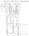
- the above-mentioned binary combined logical circuit is constructed with the connections between the basic binary gates such as AND, OR, NOT, NAND, NOR and EXOR gates as shown in Fig. 3.
- the above-mentioned sequential circuits are composed with the combined circuit and a memory circuit and the connection between them as shown in Fig. 4, and the combined circuit is constructed with the basic binary gates such as AND, OR, NOT, NAND, NOR and EXOR gates.
- binary combinational logic circuits are characterized in that they are composed with an input layer, a connecting layer, an AND layer and an OR layer as shown in Fig. 5.
- binary combinational logic circuits are also characterized in that they are composed with an input layer, a connecting layer, an OR layer and AND layer as shown in Fig. 6.
- the above binary combinational logic circuits are also characterized in that they are composed with an input layer, a connecting layer, an intermediate NOR layer and an outputting NOR layer as shown in Fig. 8.
- the above binary combinational logic circuits are also characterized in that they are composed with an input layer, a connecting layer, an intermediate EXOR layer and an outputting EXOR layer as shown in Fig. 9.
- any logic function is expressed with logical sum form (composed with AND-OR circuit shown in Fig. 5).
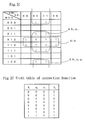
- a logic function shown in Fig. 10 becomes expressed in Eq.(2) by simplifying with a Karnaugh map shown in Fig. 11.
- Z X 1 X 2 + X 2 X 3 + X 2 X 3 X 4
- Eq.(2) The logic function shown in Eq.(2) is expressed in a block diagram shown in Fig. 12 by applying an AND-OR network.
- the connecting states between an input layer and an AND layer are determined in any one of the following four connected states in accordance to the logic function, namely:
- any logical function having n variables can be realized with an AND-OR network consisting of at most 2 (n-1) +1 AND gates.
- the connections between input layer and AND layer are realized by applying any one of the above-mentioned connections.
- the above connected conditions can be expressed by applying a pseudo-neuron (hereinafter "PN").
- PN pseudo-neuron
- the connected conditions between inputs and outputs in the pseudo-neuron are expressed with a threshold function shown in Eq.(3) or Eq.(4).
- Y ij 1 1 + e - (WijXi - ⁇ ij) wherein,
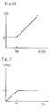
- the output from the pseudo-neuron takes either 1 or 0 in accordance to weight factor W ij and threshold ⁇ ij as shown in Fig. 14.
- the network shown in Fig. 15 is stratum-like which is composed of an input layer, a pseudo-neuron layer, an AND layer and an OR layer, and each layer is composed of adequate numbers of gates without any connection in each layer itself. Further, the connection between each layer is limited only in one direction (namely, a feed-forward type) from one input layer to output layer. In gates of each layer excepting the connection between any input layer and any pseudo-neuron layer, the connection with the forwardly placed gate is specified as binary 1.
- the response function of the PN is approximated by a Sigmoid function, and AND, OR gates are approximated by continuous valued minimum, maximum functions, many algorithms, for example, such as the error back propagation method, can be used. However, modification or learning is performed only by applying weights and thresholds of the PN.
- a learning algorithm for connected conditions between input layer and AND layer in the binary system is derived as follows.
- ⁇ W and ⁇ ⁇ are defined to take only positive values.
- ⁇ W and ⁇ ⁇ are defined to take only positive values.
- Fig. 15 For simplification, one network requiring only one output shown in Fig. 15 is considered.
- each OR gate is approximated by following continuous functions shown in Eq.(11).
- ⁇ W ij -2(Z-T)Sgn(AND j -M)Sgn(m-Y ij )X i
- ⁇ ij (Z-T)Sgn(AND j -M)Sgn(m-Y ij )
- the learning rules can be realized with logic circuits.
- the modification is limited to 1,-1 or 0 which represent that current weights and thresholds are increased, decreased or held as much as one unit, and the one unit is defined as 1 for weights and 2 for thresholds.
- the learning algorithm is composed only with logical operations between inputs, output signals, teacher's signals, outputs from AND layers and outputs from PNs, and gives a learning signal against PNs whether to increase or to decrease or to hold respective weights and thresholds.
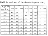
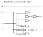
- the logic circuit for the learning signals shown in Eqs.(17) and (18) is expressed as shown in Fig. 23, and the logic circuit shown in Fig. 23 gives 0 or 1 or HP according to the above-described learning algorithm.
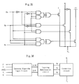
- the learning circuit is expressed as shown in Fig. 33.
- the connecting circuit is expressed as shown in Fig. 35, and the block diagram of the whole learning circuits using PN is shown in Fig. 36.
- PPE method learning algorithms applied with pseudo-potential energy method
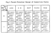
- each connected state is defined by applying the pseudo-potential energy. Further, the order from high to low of the pseudo-potential energy is assumed as follows. For 0-input, (1) 1-connected, (2) inverter-connected, (3) direct-connected, (4) 0-connected; and for 1-input, (1) 1-connected, (2) direct-connected, (3) inverter-connected and (4) 0-connected.
- S(1), S(x), S(1-x) and S(0) denote 1-connected, directly-connected, inverter-connected, and 0-connected states of a pseudo-neuron, and allocating 11, 10, 01, 00 to each of the above four connected states by applying 2 bits (q 2 , q 1 ) binary code.
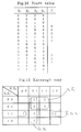
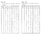
- the logical relation between Y ij and current states q 2 q 1 , input X i is expressed by the truth table shown in Fig. 37, and further the logical relation thereof is expressed by the following Eq.(24).
- Y ij q 1 X i + q 2 X i
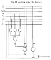
- the learning modification circuit can be realized with a circuit as shown in Fig. 40.
- the connected circuit also can be realized with a circuit as shown in Fig. 41.
- the block diagram of the whole learning circuit using the pseudo-potential energy method is shown in Fig. 42.
- a binary system for example a system shown in Fig. 5 is a multi-layered feed forward network consisting of a connecting layer, an AND layer, an OR layer.
- the learning is to change the connecting function C by applying gradient descent method or pseudo-potential energy method.
- a sequential network composed of a combinational network with a connecting layer, an AND layer, an OR layer, and a memory network with D flip-flops is considered.
- the sequential network can be represented as the following equations.
- Z(t) F(C 1 (t), X(t), D(t-1))
- D(t-1) f(C 2 (t-1), x(t-1), D(t-2))
- connection functions C 1 (t), C 2 (t-1) by gradient descent method or pseudo-potential energy method.
- the internal state D(t) at time step t can be calculated by the following equation.
- D(t) f(C 2 (t), X(t), D(t-1))
- the first binary gate and the second binary gate are defined as one of gates comprising OR, AND, NOR, NAND and EXOR gate, and the first gate is connected to the second gate in any one state among the following four connected states composed with:
- the learning is performed by selecting any one connected state among the above four states.
- an input is connected to any one gate among OR, AND, NOR, NAND and EXOR gate in any one state among the following four connected states composed with:
- the learning is performed by selecting any one connected state among the above four states.
- the learning is performed by selecting any one connected state among the above four states.
- connection between above first binary gate or an input and the second binary gate is constructed so as to select any one state among the above four connected states, at least according to the computed result between the input signal into the first binary gate and the teacher's signal for learning.
- the connection between the first binary gate (or inpute) and the second binary gate is defined by the pseudo-neuron Q and the selection of the connection (i.e., the learning) is carried out by modifying weights and thresholds of the pseudo-neuron Q.
- the systems are comprised with an input layer letting a plural of binary input data input, an AND layer having a plural of AND gates, an OR layer having a plural of OR gates letting the outputs from the AND layer input, an output layer inputting the outputs from the OR layer and a connecting layer having pseudo-neurons Q provided between the input layer and the AND layer, and the connections between the input layer and the AND layer are selected among the following connected states:
- the system is comprised with an input layer letting a plural of binary input data input, an OR layer having a plural of OR gates, an AND layer having a plural of AND gates letting the output from the OR layer input therein, an output layer inputting the outputs from the AND layer, and a connecting layer having pseudo-neurons Q provided between the input layer and the OR layer, and the connections between the input layer and the OR layer are selected among the following four connected states:
- the system is comprised with an input layer letting a plural of binary data input, an intermediate NAND layer having a plural of NAND gates, an output NAND layer having a plural of NAND gates inputting the output from the intermediate NAND layer, an output layer inputting the output from the output NAND layer and a connecting layer having pseudo-neurons Q provided between the input layer and the intermediate NAND layer, and the connections between the input layer and the intermediate NAND layer selected among the following connected states:
- the system is comprised with an input layer letting a plural of binary data input, an intermediate NOR layer having a plural of NOR gates, an output NOR layer having a plural of NOR gates inputting the output from the intermediate NOR layer, an output layer inputting the output from the output NOR layer and a connecting layer having pseudo-neurons Q provided between the input layer and the intermediate NOR layer selected from among the following connected states:
- the system is comprised with an input layer letting a plural of binary data input, an intermediate EXOR layer having a plural of EXOR gates, an output EXOR layer having a plural of EXOR gates inputting the output from the intermediate EXOR layer, an output layer inputting the output from the output EXOR layer and a connecting layer having pseudo-neurons Q provided between the input layer and the intermediate EXOR layer, and both layers are connected by any method selected from the following four connected states:
- these learning methods are expected to be used widely in image processing, voice processing, natural word processing and motion control.
- This invention provides learning methods in binary systems by modifying the connected states of the circuit among each basic binary gate in binary combined logical and sequential circuits composed with basic binary gates such as AND, OR, NOT, NAND, NOR and EXOR gates.
- basic binary gates such as AND, OR, NOT, NAND, NOR and EXOR gates.
Landscapes
- Engineering & Computer Science (AREA)
- Physics & Mathematics (AREA)
- Theoretical Computer Science (AREA)
- Health & Medical Sciences (AREA)
- Life Sciences & Earth Sciences (AREA)
- Biomedical Technology (AREA)
- Biophysics (AREA)
- General Physics & Mathematics (AREA)
- General Engineering & Computer Science (AREA)
- Software Systems (AREA)
- Evolutionary Computation (AREA)
- General Health & Medical Sciences (AREA)
- Molecular Biology (AREA)
- Computing Systems (AREA)
- Computational Linguistics (AREA)
- Artificial Intelligence (AREA)
- Mathematical Physics (AREA)
- Data Mining & Analysis (AREA)
- Neurology (AREA)
- Business, Economics & Management (AREA)
- Educational Administration (AREA)
- Educational Technology (AREA)
- Logic Circuits (AREA)
- Image Analysis (AREA)
- Electrically Operated Instructional Devices (AREA)
- Image Processing (AREA)
- Feedback Control In General (AREA)
- Character Discrimination (AREA)
Applications Claiming Priority (2)
| Application Number | Priority Date | Filing Date | Title |
|---|---|---|---|
| US08/744,299 US6061673A (en) | 1996-11-06 | 1996-11-06 | Learning methods in binary systems |
| US744299 | 1996-11-06 |
Publications (2)
| Publication Number | Publication Date |
|---|---|
| EP0841621A1 true EP0841621A1 (de) | 1998-05-13 |
| EP0841621B1 EP0841621B1 (de) | 2002-06-12 |
Family
ID=24992201
Family Applications (1)
| Application Number | Title | Priority Date | Filing Date |
|---|---|---|---|
| EP97119287A Expired - Lifetime EP0841621B1 (de) | 1996-11-06 | 1997-11-04 | Lernverfahren in Binärsystemen |
Country Status (10)
| Country | Link |
|---|---|
| US (1) | US6061673A (de) |
| EP (1) | EP0841621B1 (de) |
| JP (1) | JPH10320369A (de) |
| KR (1) | KR19980042174A (de) |
| CN (1) | CN1182246A (de) |
| CA (1) | CA2219594C (de) |
| DE (2) | DE841621T1 (de) |
| IL (1) | IL122099A (de) |
| RU (1) | RU2168713C2 (de) |
| TW (1) | TW326507B (de) |
Cited By (2)
| Publication number | Priority date | Publication date | Assignee | Title |
|---|---|---|---|---|
| EP0978791A4 (de) * | 1998-02-20 | 2000-07-05 | Sowa Inst Of Technology Co Ltd | Verfahren zum erlernen des binären systems |
| WO2001011558A1 (en) * | 1999-08-05 | 2001-02-15 | Sowa Institute Of Technology Co., Ltd. | Learning methods in binary systems |
Families Citing this family (7)
| Publication number | Priority date | Publication date | Assignee | Title |
|---|---|---|---|---|
| DE69731222T2 (de) * | 1997-08-08 | 2005-03-10 | Bridgestone Corp. | Verfahren zum entwerfen von reifen, optimierungsanalysereinrichtung und speichermedium zur aufnahme des optimierungsanalyseprogramms |
| US7420969B2 (en) * | 2000-11-29 | 2008-09-02 | Rmi Corporation | Network switch with a parallel shared memory |
| US7072345B2 (en) * | 2000-11-29 | 2006-07-04 | Raza Microelectronics, Inc | Programmable integrated circuit for use in a network switch |
| US7293002B2 (en) * | 2001-06-19 | 2007-11-06 | Ohio University | Self-organizing data driven learning hardware with local interconnections |
| US11494634B2 (en) * | 2020-05-13 | 2022-11-08 | International Business Machines Corporation | Optimizing capacity and learning of weighted real-valued logic |
| US12045319B2 (en) | 2020-05-13 | 2024-07-23 | International Business Machines Corporation | First-order logical neural networks with bidirectional inference |
| JP2025516545A (ja) * | 2022-05-09 | 2025-05-30 | メムコンピューティング インコーポレイテッド | 複数の端末論理ゲートから形成された複数の層を有する深層ニューラルネットワーク |
Citations (3)
| Publication number | Priority date | Publication date | Assignee | Title |
|---|---|---|---|---|
| WO1992004687A1 (de) * | 1990-09-11 | 1992-03-19 | Siemens Aktiengesellschaft | Verfahren und anordnung zur boole'schen realisierung neuronaler netze vom adaline-typ |
| EP0476159A1 (de) * | 1990-09-15 | 1992-03-25 | International Business Machines Corporation | Programmierbare Schaltung für eine neurale Logik |
| WO1992012497A1 (fr) * | 1991-01-02 | 1992-07-23 | Claude Abin | Reseau neuronal a operateurs binaires et procedes pour sa realisation |
Family Cites Families (13)
| Publication number | Priority date | Publication date | Assignee | Title |
|---|---|---|---|---|
| KR910002134B1 (ko) * | 1986-11-29 | 1991-04-04 | 대우전자 주식회사 | 한자표시가 가능한 엠 에스 엑스(msx) 컴퓨터 |
| US4807168A (en) * | 1987-06-10 | 1989-02-21 | The United States Of America As Represented By The Administrator, National Aeronautics And Space Administration | Hybrid analog-digital associative neural network |
| KR900007636Y1 (ko) * | 1988-02-12 | 1990-08-23 | 대우자동차 주식회사 | 차량의 선반장치 |
| US5050095A (en) * | 1988-05-31 | 1991-09-17 | Honeywell Inc. | Neural network auto-associative memory with two rules for varying the weights |
| KR900702462A (ko) * | 1988-09-12 | 1990-12-07 | 야마모또 다꾸마 | 네트워크 구성 데이타 처리장치의 학습처리 방식 |
| US4941122A (en) * | 1989-01-12 | 1990-07-10 | Recognition Equipment Incorp. | Neural network image processing system |
| US5167006A (en) * | 1989-12-29 | 1992-11-24 | Ricoh Company, Ltd. | Neuron unit, neural network and signal processing method |
| US5212765A (en) * | 1990-08-03 | 1993-05-18 | E. I. Du Pont De Nemours & Co., Inc. | On-line training neural network system for process control |
| KR930004271B1 (ko) * | 1990-09-18 | 1993-05-22 | 금성일렉트론 주식회사 | 바이너리 카운터 |
| US5226092A (en) * | 1991-06-28 | 1993-07-06 | Digital Equipment Corporation | Method and apparatus for learning in a neural network |
| JPH05210649A (ja) * | 1992-01-24 | 1993-08-20 | Mitsubishi Electric Corp | 神経回路網表現装置 |
| US5455891A (en) * | 1993-10-04 | 1995-10-03 | Georgia Tech Research Corporation | System and method for a learning neural network for generating random directions for weight changes |
| JP2690702B2 (ja) * | 1994-09-13 | 1997-12-17 | 日本電気株式会社 | 自己組織化装置 |
-
1996
- 1996-11-06 US US08/744,299 patent/US6061673A/en not_active Expired - Fee Related
- 1996-11-13 TW TW085113850A patent/TW326507B/zh active
-
1997
- 1997-10-28 CA CA002219594A patent/CA2219594C/en not_active Expired - Fee Related
- 1997-11-04 DE DE0841621T patent/DE841621T1/de active Pending
- 1997-11-04 CN CN97122513A patent/CN1182246A/zh active Pending
- 1997-11-04 EP EP97119287A patent/EP0841621B1/de not_active Expired - Lifetime
- 1997-11-04 DE DE69713247T patent/DE69713247T2/de not_active Expired - Fee Related
- 1997-11-04 IL IL12209997A patent/IL122099A/xx not_active IP Right Cessation
- 1997-11-05 RU RU97118609/09A patent/RU2168713C2/ru not_active IP Right Cessation
- 1997-11-05 JP JP9320297A patent/JPH10320369A/ja active Pending
- 1997-11-06 KR KR1019970058581A patent/KR19980042174A/ko not_active Ceased
Patent Citations (3)
| Publication number | Priority date | Publication date | Assignee | Title |
|---|---|---|---|---|
| WO1992004687A1 (de) * | 1990-09-11 | 1992-03-19 | Siemens Aktiengesellschaft | Verfahren und anordnung zur boole'schen realisierung neuronaler netze vom adaline-typ |
| EP0476159A1 (de) * | 1990-09-15 | 1992-03-25 | International Business Machines Corporation | Programmierbare Schaltung für eine neurale Logik |
| WO1992012497A1 (fr) * | 1991-01-02 | 1992-07-23 | Claude Abin | Reseau neuronal a operateurs binaires et procedes pour sa realisation |
Non-Patent Citations (2)
| Title |
|---|
| ELIASHBERG V: "A RELATIONSHIP BETWEEN NEURAL NETWORKS AND PROGRAMMABLE LOGIC ARRAYS", PROCEEDINGS OF THE INTERNATIONAL CONFERENCE ON NEURAL NETWORKS (ICN, SAN FRANCISCO, MAR. 28 - APR. 1, 1993, vol. 3, 28 March 1993 (1993-03-28), INSTITUTE OF ELECTRICAL AND ELECTRONICS ENGINEERS, pages 1333 - 1337, XP000379470 * |
| VESELKO GUSTIN: "ARTIFICIAL NEURAL NETWORK REALIZATION WITH PROGRAMMABLE LOGIC CIRCUIT", MICROPROCESSING AND MICROPROGRAMMING, vol. 35, no. 1 / 05, 1 September 1992 (1992-09-01), pages 187 - 192, XP000325123 * |
Cited By (3)
| Publication number | Priority date | Publication date | Assignee | Title |
|---|---|---|---|---|
| EP0978791A4 (de) * | 1998-02-20 | 2000-07-05 | Sowa Inst Of Technology Co Ltd | Verfahren zum erlernen des binären systems |
| WO2001011558A1 (en) * | 1999-08-05 | 2001-02-15 | Sowa Institute Of Technology Co., Ltd. | Learning methods in binary systems |
| AU765460B2 (en) * | 1999-08-05 | 2003-09-18 | Sowa Institute Of Technology Co., Ltd. | Learning methods in binary systems |
Also Published As
| Publication number | Publication date |
|---|---|
| JPH10320369A (ja) | 1998-12-04 |
| CA2219594C (en) | 2002-04-16 |
| MX9708565A (es) | 1998-06-30 |
| CN1182246A (zh) | 1998-05-20 |
| CA2219594A1 (en) | 1998-05-06 |
| EP0841621B1 (de) | 2002-06-12 |
| RU2168713C2 (ru) | 2001-06-10 |
| US6061673A (en) | 2000-05-09 |
| DE69713247D1 (de) | 2002-07-18 |
| KR19980042174A (ko) | 1998-08-17 |
| TW326507B (en) | 1998-02-11 |
| IL122099A (en) | 2001-01-28 |
| DE841621T1 (de) | 1998-11-12 |
| DE69713247T2 (de) | 2003-02-06 |
| IL122099A0 (en) | 1998-04-05 |
Similar Documents
| Publication | Publication Date | Title |
|---|---|---|
| Kolen et al. | A field guide to dynamical recurrent networks | |
| US5165010A (en) | Information processing system | |
| US5095457A (en) | Digital multiplier employing CMOS transistors | |
| JP2662000B2 (ja) | 神経回路網およびその回路網に用いる回路 | |
| KR930002792B1 (ko) | 뉴우런 아키텍쳐(neuron architecture) | |
| EP0841621B1 (de) | Lernverfahren in Binärsystemen | |
| US5347613A (en) | MOS multi-layer neural network including a plurality of hidden layers interposed between synapse groups for performing pattern recognition | |
| Lu et al. | A multi-sieving neural network architecture that decomposes learning tasks automatically | |
| JPH04182769A (ja) | デジタル・ニューロプロセッサ | |
| Ciampi et al. | Statistical models as building blocks of neural networks | |
| WO2001011558A1 (en) | Learning methods in binary systems | |
| MXPA97008565A (en) | Learning method in binar systems | |
| ZA200102507B (en) | Learning methods in binary systems. | |
| Tsoi et al. | Building MLP networks by construction | |
| El-Bakry et al. | Simplification and implementation of boolean functions | |
| JPH0243665A (ja) | ニューラルネットワーク装置 | |
| JP3130913B2 (ja) | 信号処理装置 | |
| HABIB et al. | O FT SOT EN CET ENGINEERING | |
| Malhotra et al. | Evaluation of electronic artificial neural network implementations | |
| Beiu | On higher order noise immune perceptrons | |
| Howells et al. | Novel neural architectures for recognition of handwritten characters | |
| JP3343626B2 (ja) | ファジィ推論のためのニューラルネットワーク | |
| JP3126762B2 (ja) | ニューラルネットワーク | |
| Girau et al. | FPGA-Targeted Neural Architecture for Embedded Alertness Detection. | |
| JP3263955B2 (ja) | しきい値回路 |
Legal Events
| Date | Code | Title | Description |
|---|---|---|---|
| PUAI | Public reference made under article 153(3) epc to a published international application that has entered the european phase |
Free format text: ORIGINAL CODE: 0009012 |
|
| AK | Designated contracting states |
Kind code of ref document: A1 Designated state(s): DE FR GB IE NL |
|
| AX | Request for extension of the european patent |
Free format text: AL;LT;LV;MK;RO;SI |
|
| EL | Fr: translation of claims filed | ||
| TCNL | Nl: translation of patent claims filed | ||
| DET | De: translation of patent claims | ||
| 17P | Request for examination filed |
Effective date: 19981113 |
|
| AKX | Designation fees paid |
Free format text: DE FR GB IE NL |
|
| RBV | Designated contracting states (corrected) |
Designated state(s): DE FR GB IE NL |
|
| 17Q | First examination report despatched |
Effective date: 19990224 |
|
| GRAG | Despatch of communication of intention to grant |
Free format text: ORIGINAL CODE: EPIDOS AGRA |
|
| RTI1 | Title (correction) |
Free format text: LEARNING METHOD IN BINARY SYSTEMS |
|
| GRAG | Despatch of communication of intention to grant |
Free format text: ORIGINAL CODE: EPIDOS AGRA |
|
| GRAH | Despatch of communication of intention to grant a patent |
Free format text: ORIGINAL CODE: EPIDOS IGRA |
|
| GRAH | Despatch of communication of intention to grant a patent |
Free format text: ORIGINAL CODE: EPIDOS IGRA |
|
| GRAA | (expected) grant |
Free format text: ORIGINAL CODE: 0009210 |
|
| AK | Designated contracting states |
Kind code of ref document: B1 Designated state(s): DE FR GB IE NL |
|
| REG | Reference to a national code |
Ref country code: GB Ref legal event code: FG4D |
|
| REF | Corresponds to: |
Ref document number: 69713247 Country of ref document: DE Date of ref document: 20020718 |
|
| REG | Reference to a national code |
Ref country code: IE Ref legal event code: FG4D |
|
| ET | Fr: translation filed | ||
| PGFP | Annual fee paid to national office [announced via postgrant information from national office to epo] |
Ref country code: GB Payment date: 20021024 Year of fee payment: 6 |
|
| PGFP | Annual fee paid to national office [announced via postgrant information from national office to epo] |
Ref country code: NL Payment date: 20021118 Year of fee payment: 6 Ref country code: FR Payment date: 20021118 Year of fee payment: 6 |
|
| PGFP | Annual fee paid to national office [announced via postgrant information from national office to epo] |
Ref country code: IE Payment date: 20021129 Year of fee payment: 6 |
|
| PGFP | Annual fee paid to national office [announced via postgrant information from national office to epo] |
Ref country code: DE Payment date: 20021227 Year of fee payment: 6 |
|
| PLBE | No opposition filed within time limit |
Free format text: ORIGINAL CODE: 0009261 |
|
| STAA | Information on the status of an ep patent application or granted ep patent |
Free format text: STATUS: NO OPPOSITION FILED WITHIN TIME LIMIT |
|
| 26N | No opposition filed |
Effective date: 20030313 |
|
| PG25 | Lapsed in a contracting state [announced via postgrant information from national office to epo] |
Ref country code: IE Free format text: LAPSE BECAUSE OF NON-PAYMENT OF DUE FEES Effective date: 20031104 Ref country code: GB Free format text: LAPSE BECAUSE OF NON-PAYMENT OF DUE FEES Effective date: 20031104 |
|
| PG25 | Lapsed in a contracting state [announced via postgrant information from national office to epo] |
Ref country code: NL Free format text: LAPSE BECAUSE OF NON-PAYMENT OF DUE FEES Effective date: 20040601 |
|
| PG25 | Lapsed in a contracting state [announced via postgrant information from national office to epo] |
Ref country code: DE Free format text: LAPSE BECAUSE OF NON-PAYMENT OF DUE FEES Effective date: 20040602 |
|
| GBPC | Gb: european patent ceased through non-payment of renewal fee |
Effective date: 20031104 |
|
| PG25 | Lapsed in a contracting state [announced via postgrant information from national office to epo] |
Ref country code: FR Free format text: LAPSE BECAUSE OF NON-PAYMENT OF DUE FEES Effective date: 20040730 |
|
| NLV4 | Nl: lapsed or anulled due to non-payment of the annual fee |
Effective date: 20040601 |
|
| REG | Reference to a national code |
Ref country code: IE Ref legal event code: MM4A |
|
| REG | Reference to a national code |
Ref country code: FR Ref legal event code: ST |