EP0841742A2 - Circuit de conversion de puissance - Google Patents
Circuit de conversion de puissance Download PDFInfo
- Publication number
- EP0841742A2 EP0841742A2 EP97810770A EP97810770A EP0841742A2 EP 0841742 A2 EP0841742 A2 EP 0841742A2 EP 97810770 A EP97810770 A EP 97810770A EP 97810770 A EP97810770 A EP 97810770A EP 0841742 A2 EP0841742 A2 EP 0841742A2
- Authority
- EP
- European Patent Office
- Prior art keywords
- converter
- converters
- load
- output
- circuit
- Prior art date
- Legal status (The legal status is an assumption and is not a legal conclusion. Google has not performed a legal analysis and makes no representation as to the accuracy of the status listed.)
- Granted
Links
Images


Classifications
-
- H—ELECTRICITY
- H02—GENERATION; CONVERSION OR DISTRIBUTION OF ELECTRIC POWER
- H02M—APPARATUS FOR CONVERSION BETWEEN AC AND AC, BETWEEN AC AND DC, OR BETWEEN DC AND DC, AND FOR USE WITH MAINS OR SIMILAR POWER SUPPLY SYSTEMS; CONVERSION OF DC OR AC INPUT POWER INTO SURGE OUTPUT POWER; CONTROL OR REGULATION THEREOF
- H02M7/00—Conversion of AC power input into DC power output; Conversion of DC power input into AC power output
- H02M7/42—Conversion of DC power input into AC power output without possibility of reversal
- H02M7/44—Conversion of DC power input into AC power output without possibility of reversal by static converters
- H02M7/48—Conversion of DC power input into AC power output without possibility of reversal by static converters using discharge tubes with control electrode or semiconductor devices with control electrode
- H02M7/483—Converters with outputs that each can have more than two voltages levels
- H02M7/49—Combination of the output voltage waveforms of a plurality of converters
Definitions
- the invention relates to the field of power electronics. It is based on a converter circuit arrangement according to the preamble of the first claim.
- a fine-stage output voltage can be achieved with the concepts according to the prior art through a large number of individual stages, the output voltages of which are added.
- the GTOs required, their wiring and, in particular, the expense for the transformers cause the manufacturing price of the circuit arrangement to rise considerably.
- the object of the present invention is to provide a converter circuit arrangement with which a finely graded output voltage can be achieved with fewer transformers and can therefore be produced more cost-effectively.
- the essence of the invention is therefore that the secondary windings of the output transformers are connected in series with the primary winding of a load transformer and the load-side connections of a first converter.
- This allows the transformation ratios of the output transformers to one another, e.g. graded binary or ternary.
- converter stages with different output voltages are available, and a fine-stage approximation to a sinusoidal output voltage can be achieved.
- the power converters can have the structure of a three-point or a two-point inverter.
- the individual converters can also consist of two Partial converters can be constructed. In this case, the primary winding of the output transformers is arranged between the two partial converters.
- a major advantage of the new circuit arrangement is that the advantages of series connection of GTOs (redundancy, availability) can be used economically in a wide range of system performance.
- FIG. 1 shows a first embodiment of the invention. 1 with a DC voltage intermediate circuit is designated. This is represented by two DC voltage sources 11, each with half the intermediate circuit voltage U zk / 2.
- a first converter 2 and two further converters 3 are connected in parallel to the DC voltage intermediate circuit 1.
- the two converters 3 each have an output transformer 5 at their load-side output.
- One connection of the primary winding 6 of the output transformers 5 is connected to the center of the intermediate circuit and the other to the load-side output of the converter 3.
- a load transformer 8 is provided, which feeds a load circuit 4.
- the load circuit 4 can represent, for example, a railway network, while the DC voltage intermediate circuit 1 is fed by a voltage supply network.
- the primary winding 9 of the load transformer 8 forms a series circuit with the secondary windings 7 of the output transformers 5 and the load-side output of the first converter 2. Thus, all the output voltages of the converters 2 and 3 are summed up over the primary winding of the load transformer 8 and transmitted to the load circuit 4 with a specific transmission ratio via the load transformer 8.
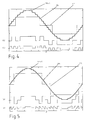
- FIG. 4 shows the corresponding voltage profiles with transmission ratios of the output transformers 5 of 4: 1 and 2: 1.
- Figure 5 shows corresponding curves for gear ratios 9: 1 and 3: 1.
- U1 denotes the ideal output voltage of the first converter 2, U2 that of the converter 3 whose output transformer has a conversion ratio of 2: 1 or 3: 1, and U3 that of the converter 3 whose output transformer has a conversion ratio of 4: 1 or 9: 1 has.
- Utot represents the sum of the voltages U1, U2 and U3 and Uo the sinusoidal voltage curve to be approximated.
- the binary or ternary gradation of the gear ratios is appropriate because the calculation of the control pattern and the resulting control command sequences are simple. Other, even odd gear ratios would also be conceivable and did not change the basic circuit arrangement.
- FIG. 2 shows a further exemplary embodiment of the invention, in which the converters are each made up of two partial converters 2.1, 2.2, 3.1, 3.2.
- the primary windings 6 of the output transformers 5 are no longer connected to the output of the converter and ground, but rather are connected between two partial converters 3.1 and 3.2.
- the primary winding 9 of the load transformer 8 is in turn connected in series with the secondary windings 7, but in this case also with the two partial converters 2.1 and 2.2 of the first converter.
- the output voltages of all converters or output transformers are thus in turn summed and transmitted to the load circuit via the load transformer 8.
- the advantage of the arrangement according to FIG. 2 is that the output voltage can be controlled in terms of the phase and phase shift of the partial converter of a converter block in terms of amplitude and phase position relative to the network to be fed.
- the adjacent partial converters 2.1, 2.2 or 3.1, 3.2 are driven exactly inverted.
- the output voltage is doubled compared to the arrangement according to FIG. 1.
- the control i.e. lowering or increasing the output voltage
- the phase angle of the output voltage with respect to the mains voltage is generated by jointly pivoting all 6 pulse patterns by the angle ⁇ .
- the relationship is that the ratio of the instantaneous output voltage to the maximum output voltage is cos ( ⁇ )
- an output filter 12 in the form of an RC element is also provided. Its job is to filter small unavoidable switching offsets of those converters that should theoretically switch at the same time.
- FIGS. 1 and 2 use three-point inverters as converter blocks. It is of course also possible to set up a corresponding circuit arrangement with two-point inverters.
- Figure 3 shows a corresponding embodiment.
- the circuit is mirror-symmetrical and includes an upper half and a lower half. In the case of full control, the converters in the upper half are controlled in the inverse of those in the lower half. Control of the output voltage and the phase angle is obtained analogously to the example according to FIG. 2 by phase-shifted clocking of the upper converter groups with respect to the lower converter groups.
- the secondary winding of the load transformer in the upper half is connected in series with that in the lower half.
- the invention results in a circuit arrangement with which a good approximation to the sine function can be achieved in an economical manner.
Landscapes
- Engineering & Computer Science (AREA)
- Power Engineering (AREA)
- Inverter Devices (AREA)
- Ac-Ac Conversion (AREA)
- Dc-Dc Converters (AREA)
- Seal Device For Vehicle (AREA)
- Table Devices Or Equipment (AREA)
- Automatic Analysis And Handling Materials Therefor (AREA)
- Rectifiers (AREA)
- Electric Propulsion And Braking For Vehicles (AREA)
- Nitrogen Condensed Heterocyclic Rings (AREA)
- Saccharide Compounds (AREA)
Applications Claiming Priority (2)
| Application Number | Priority Date | Filing Date | Title |
|---|---|---|---|
| DE19646085 | 1996-11-08 | ||
| DE19646085A DE19646085A1 (de) | 1996-11-08 | 1996-11-08 | Stromrichterschaltungsanordnung |
Publications (3)
| Publication Number | Publication Date |
|---|---|
| EP0841742A2 true EP0841742A2 (fr) | 1998-05-13 |
| EP0841742A3 EP0841742A3 (fr) | 2000-03-01 |
| EP0841742B1 EP0841742B1 (fr) | 2002-03-27 |
Family
ID=7811027
Family Applications (1)
| Application Number | Title | Priority Date | Filing Date |
|---|---|---|---|
| EP97810770A Expired - Lifetime EP0841742B1 (fr) | 1996-11-08 | 1997-10-13 | Circuit de conversion de puissance |
Country Status (6)
| Country | Link |
|---|---|
| US (1) | US6052296A (fr) |
| EP (1) | EP0841742B1 (fr) |
| AT (1) | ATE215280T1 (fr) |
| CA (1) | CA2216491A1 (fr) |
| DE (2) | DE19646085A1 (fr) |
| NO (1) | NO975120L (fr) |
Cited By (1)
| Publication number | Priority date | Publication date | Assignee | Title |
|---|---|---|---|---|
| WO2010033759A1 (fr) * | 2008-09-18 | 2010-03-25 | Superior Electric Holding Group Llc | Régulateur de tension binaire |
Families Citing this family (2)
| Publication number | Priority date | Publication date | Assignee | Title |
|---|---|---|---|---|
| US7830687B2 (en) * | 2006-07-13 | 2010-11-09 | Florida State University Research Foundation, Inc. | Adaptive power electronics interface for hybrid energy systems |
| JP2017175862A (ja) * | 2016-03-25 | 2017-09-28 | 東芝三菱電機産業システム株式会社 | 電力変換装置 |
Family Cites Families (6)
| Publication number | Priority date | Publication date | Assignee | Title |
|---|---|---|---|---|
| US3919619A (en) * | 1974-06-05 | 1975-11-11 | Gen Motors Corp | Apparatus for generating three-phase sinusoidal voltages |
| CA2013492C (fr) * | 1989-03-31 | 1995-07-25 | Shigeru Tanaka | Convertisseur d'alimentation multitension et multifrequence |
| US4994953A (en) * | 1989-08-15 | 1991-02-19 | Sundstrand Corporation | DC power supply for high power applications |
| US5041957A (en) * | 1989-12-20 | 1991-08-20 | Sundstrand Corporation | Stepped-waveform inverter with six subinverters |
| US5008797A (en) * | 1989-12-20 | 1991-04-16 | Sundstrand Corporation | Power converter utilizing line replaceable units |
| DE4225269A1 (de) * | 1992-07-31 | 1994-02-03 | Asea Brown Boveri | Verfahren zur Dämpfung von Netzoberschwingungen und eine Netzkupplung |
-
1996
- 1996-11-08 DE DE19646085A patent/DE19646085A1/de not_active Withdrawn
-
1997
- 1997-08-29 US US08/921,387 patent/US6052296A/en not_active Expired - Fee Related
- 1997-09-25 CA CA002216491A patent/CA2216491A1/fr not_active Abandoned
- 1997-10-13 DE DE59706744T patent/DE59706744D1/de not_active Expired - Fee Related
- 1997-10-13 EP EP97810770A patent/EP0841742B1/fr not_active Expired - Lifetime
- 1997-10-13 AT AT97810770T patent/ATE215280T1/de not_active IP Right Cessation
- 1997-11-07 NO NO975120A patent/NO975120L/no not_active Application Discontinuation
Cited By (2)
| Publication number | Priority date | Publication date | Assignee | Title |
|---|---|---|---|---|
| WO2010033759A1 (fr) * | 2008-09-18 | 2010-03-25 | Superior Electric Holding Group Llc | Régulateur de tension binaire |
| US8035358B2 (en) | 2008-09-18 | 2011-10-11 | Superior Electric Holding Group Llc | Binary voltage regulator |
Also Published As
| Publication number | Publication date |
|---|---|
| US6052296A (en) | 2000-04-18 |
| NO975120D0 (no) | 1997-11-07 |
| NO975120L (no) | 1998-05-11 |
| DE59706744D1 (de) | 2002-05-02 |
| CA2216491A1 (fr) | 1998-05-08 |
| DE19646085A1 (de) | 1998-05-14 |
| ATE215280T1 (de) | 2002-04-15 |
| EP0841742B1 (fr) | 2002-03-27 |
| EP0841742A3 (fr) | 2000-03-01 |
Similar Documents
| Publication | Publication Date | Title |
|---|---|---|
| EP0802617A2 (fr) | Circuit électronique de puissance | |
| DE2350778C2 (de) | Mehrphasige Stromrichterstation für eine HGÜ-Anlage | |
| DE2843528C2 (fr) | ||
| EP0852841B1 (fr) | Transformateur oblique de puissance elevee, compatible avec le reseau, pilote par convertisseur de courant et appliquant une tension | |
| DE69125894T2 (de) | Optimiertes 18-Puls AC/DC, oder DC/AC, Konvertersystem | |
| EP2928060A1 (fr) | Circuit de convertisseur modulaire doté de sous-modules présentant différentes capacités de commutation | |
| EP0841742B1 (fr) | Circuit de conversion de puissance | |
| WO2019007502A1 (fr) | Onduleur à plusieurs niveaux | |
| DE2800928C3 (de) | Schaltungsanordnung für den Fahrbetrieb sowie für den Nutz- und Widerstandsbremsbetrieb einer aus einem Gleichspannungsnetz gespeisten Wechselstrommaschine | |
| EP0989016B1 (fr) | Circuit de conversion de puissance avec configuration variable pour applications à la traction | |
| EP0428035B1 (fr) | Cyclo-convertisseur triphasé | |
| DE102011085559A1 (de) | Spannungswandler mit einer ersten Parallelschaltung | |
| DE642679C (de) | Mehrphasiger Netzkupplungstransformator mit regelbarer Spannung sowohl der Groesse als auch der Phasenlage nach, dessen Wicklungen je Phase an einem Wicklungsende mit Anzapfungen versehen sind | |
| DE3231945C2 (fr) | ||
| DE2646745C3 (de) | Schaltungsanordnung zur Speisung eines Gleichspannungsverbrauchers | |
| DE1950319B2 (de) | Elektrisches Schaltgerät mit parallelgeschalteten Strombahnen | |
| DE102018206448A1 (de) | Anlage und Verfahren zur Energieversorgung, insbesondere zur Bahnenergieversorgung | |
| EP1480322B1 (fr) | Procédé de control d'un convertisseur de puissance | |
| DE911512C (de) | Anordnung zur Verbesserung des Leistungsfaktors bei der Spannungsregelung von Stromrichtern | |
| DE9408504U1 (de) | Frequenzumrichter | |
| DE10246526B4 (de) | Verfahren zur Ansteuerung eines Matrixumrichters | |
| DE1613518A1 (de) | Kraftuebertragungsanlage fuer hochgespannten Gleichstrom | |
| DE1438773C (de) | Wahlweise aus einer Wechselstrom oder Gleichstromfahrleitung speisbares elektn sches Triebfahrzeug mit Gleichstrom Fahrmotoren | |
| DE3636902C2 (fr) | ||
| DE1813853C3 (de) | Anordnung zur Anzapfung der Verbindungsleitung einer Hochspannungs-Gleichstrom-Übertragung (HGÜ) in Serienschaltung |
Legal Events
| Date | Code | Title | Description |
|---|---|---|---|
| PUAI | Public reference made under article 153(3) epc to a published international application that has entered the european phase |
Free format text: ORIGINAL CODE: 0009012 |
|
| AK | Designated contracting states |
Kind code of ref document: A2 Designated state(s): AT CH DE LI SE |
|
| PUAL | Search report despatched |
Free format text: ORIGINAL CODE: 0009013 |
|
| AK | Designated contracting states |
Kind code of ref document: A3 Designated state(s): AT BE CH DE DK ES FI FR GB GR IE IT LI LU MC NL PT SE |
|
| RAP1 | Party data changed (applicant data changed or rights of an application transferred) |
Owner name: ABB INDUSTRIE AG |
|
| 17P | Request for examination filed |
Effective date: 20000526 |
|
| AKX | Designation fees paid |
Free format text: AT CH DE LI SE |
|
| GRAG | Despatch of communication of intention to grant |
Free format text: ORIGINAL CODE: EPIDOS AGRA |
|
| 17Q | First examination report despatched |
Effective date: 20010515 |
|
| GRAG | Despatch of communication of intention to grant |
Free format text: ORIGINAL CODE: EPIDOS AGRA |
|
| GRAH | Despatch of communication of intention to grant a patent |
Free format text: ORIGINAL CODE: EPIDOS IGRA |
|
| GRAH | Despatch of communication of intention to grant a patent |
Free format text: ORIGINAL CODE: EPIDOS IGRA |
|
| GRAA | (expected) grant |
Free format text: ORIGINAL CODE: 0009210 |
|
| AK | Designated contracting states |
Kind code of ref document: B1 Designated state(s): AT CH DE LI SE |
|
| REF | Corresponds to: |
Ref document number: 215280 Country of ref document: AT Date of ref document: 20020415 Kind code of ref document: T |
|
| REG | Reference to a national code |
Ref country code: CH Ref legal event code: EP |
|
| RAP2 | Party data changed (patent owner data changed or rights of a patent transferred) |
Owner name: ABB SCHWEIZ AG |
|
| REF | Corresponds to: |
Ref document number: 59706744 Country of ref document: DE Date of ref document: 20020502 |
|
| PG25 | Lapsed in a contracting state [announced via postgrant information from national office to epo] |
Ref country code: SE Free format text: LAPSE BECAUSE OF FAILURE TO SUBMIT A TRANSLATION OF THE DESCRIPTION OR TO PAY THE FEE WITHIN THE PRESCRIBED TIME-LIMIT Effective date: 20020627 |
|
| PG25 | Lapsed in a contracting state [announced via postgrant information from national office to epo] |
Ref country code: AT Free format text: LAPSE BECAUSE OF NON-PAYMENT OF DUE FEES Effective date: 20021013 |
|
| PG25 | Lapsed in a contracting state [announced via postgrant information from national office to epo] |
Ref country code: LI Free format text: LAPSE BECAUSE OF NON-PAYMENT OF DUE FEES Effective date: 20021031 Ref country code: CH Free format text: LAPSE BECAUSE OF NON-PAYMENT OF DUE FEES Effective date: 20021031 |
|
| PLBE | No opposition filed within time limit |
Free format text: ORIGINAL CODE: 0009261 |
|
| STAA | Information on the status of an ep patent application or granted ep patent |
Free format text: STATUS: NO OPPOSITION FILED WITHIN TIME LIMIT |
|
| 26N | No opposition filed |
Effective date: 20021230 |
|
| PG25 | Lapsed in a contracting state [announced via postgrant information from national office to epo] |
Ref country code: DE Free format text: LAPSE BECAUSE OF NON-PAYMENT OF DUE FEES Effective date: 20030501 |
|
| REG | Reference to a national code |
Ref country code: CH Ref legal event code: PL |