EP0841787A2 - Synchronisation dans un récepteur multiporteur - Google Patents
Synchronisation dans un récepteur multiporteur Download PDFInfo
- Publication number
- EP0841787A2 EP0841787A2 EP97118177A EP97118177A EP0841787A2 EP 0841787 A2 EP0841787 A2 EP 0841787A2 EP 97118177 A EP97118177 A EP 97118177A EP 97118177 A EP97118177 A EP 97118177A EP 0841787 A2 EP0841787 A2 EP 0841787A2
- Authority
- EP
- European Patent Office
- Prior art keywords
- calculating
- impulse response
- signal
- response signal
- demodulator
- Prior art date
- Legal status (The legal status is an assumption and is not a legal conclusion. Google has not performed a legal analysis and makes no representation as to the accuracy of the status listed.)
- Withdrawn
Links
Images


Classifications
-
- H—ELECTRICITY
- H04—ELECTRIC COMMUNICATION TECHNIQUE
- H04L—TRANSMISSION OF DIGITAL INFORMATION, e.g. TELEGRAPHIC COMMUNICATION
- H04L27/00—Modulated-carrier systems
- H04L27/26—Systems using multi-frequency codes
- H04L27/2601—Multicarrier modulation systems
- H04L27/2647—Arrangements specific to the receiver only
- H04L27/2655—Synchronisation arrangements
- H04L27/2662—Symbol synchronisation
- H04L27/2665—Fine synchronisation, e.g. by positioning the FFT window
-
- H—ELECTRICITY
- H04—ELECTRIC COMMUNICATION TECHNIQUE
- H04L—TRANSMISSION OF DIGITAL INFORMATION, e.g. TELEGRAPHIC COMMUNICATION
- H04L27/00—Modulated-carrier systems
- H04L27/26—Systems using multi-frequency codes
- H04L27/2601—Multicarrier modulation systems
- H04L27/2647—Arrangements specific to the receiver only
- H04L27/2655—Synchronisation arrangements
Definitions
- the present invention relates to a demodulator of a receiver which uses orthogonal frequency division multiplex modulation such as in the case of digital-audio broadcasting.
- a conventional demodulator of this type is constructed as shown in Fig. 4, taking as an example a receiver for receiving radio waves of digital-audio broadcasting in conformity with European Broadcasting Union.
- a received intermediate frequency signal which was orthogonal-frequency-division-multiplex modulated (hereinafter described as OFDM modulated where applicable), is supplied to an input terminal and A/D converted by an A/D converter 1.
- the A/D converted signal is converted into parallel data by a serial/parallel converter 2.
- This parallel data is supplied to a fast Fourier transformation circuit (hereinafter described as FFT circuit) 3 whereat it is Fourier transformed to be converted from signals in a time domain into signals in a frequency domain.
- FFT circuit fast Fourier transformation circuit
- An output of the FFT circuit 3 is delay-detected by a delay detector 4 and output as a demodulated signal.
- An output from the FFT circuit 3 is also supplied to a switch circuit 5 which is controlled by a gate signal from a timing generator 17.
- the switch circuit 5 passes only a phase reference symbol (hereinafter described as PRS symbol where applicable) of the output from the FFT circuit 3.
- PRS symbol is a known fixed symbol which is referred to by the demodulator for the detection of frequency and timing.
- a pattern generator 6 generates a carrier in accordance with a conjugate complex number signal of a signal in the frequency range represented by the PRS symbol.
- the carrier generated by the pattern generator 6 in accordance with the conjugate complex number signal and a carrier received from the PRS symbol are multiplied together by a cross power calculator 7 to obtain a cross power. If the received signal frequency is in tune, the calculation results of the cross power calculator 7 indicate a frequency transfer function of the transmission path at the frequency point where the carrier is present.
- An output signal of the cross power calculator 7 is inverse Fourier transformed by an inverse fast Fourier transformation circuit (hereinafter described as IFFT circuit) 8. With this inverse Fourier transformation, the IFFT circuit 8 can output a pseudo complex impulse response signal of the transmission path.
- IFFT circuit inverse fast Fourier transformation circuit
- the complex impulse response signal output from the IFFT circuit 8 is supplied to a power calculation circuit 9 which performs a square calculation of the input complex impulse response signal to obtain a power signal.
- the power signal output from the power calculation circuit 9 is supplied to a peak position detector 13 to obtain a peak position of the input power signal, i.e., the peak level of the impulse response signal, which is supplied to a timing control circuit 14.
- the timing control circuit 14 controls via a D/A converter 15 the oscillation frequency of a voltage controlled crystal oscillator (VCXO) 16 in such a manner that the power signal or the impulse response signal becomes maximum at a target position.
- VCXO voltage controlled crystal oscillator
- a plurality of peaks may appear on an impulse response signal while a plurality of radio waves are received with a single antenna in a single frequency network (hereinafter described as SFN where applicable) environment or in a multipath environment. It is therefore difficult to converge the reception timing into an optimum one by only detecting the peak position, and interference is likely to occur between OFDM symbols.
- SFN single frequency network
- a demodulator of a receiver for receiving an orthogonal frequency division multiplex modulated signal comprises: first calculating means for calculating a transfer function of a transmission path at a frequency point where a carrier is present; second calculating means for calculating an impulse response signal from the transfer function calculated by said first calculating means; detecting means for calculating a sum of levels of the impulse response signal in a substantially and sequentially shifted window nearly equal to a guard interval period to detect a position where a maximum value of the sum is obtained; and control means for controlling a reception timing in accordance with the position of the maximum value detected by said detecting means so as to converge the position of the maximum value into a target position.
- a sum of levels of the impulse response signal is calculated in a substantially and sequentially shifted window nearly equal to a guard interval period, and a reception timing is controlled so that the position of the maximum value of the sum of the impulse response signal converges into a target position. Accordingly, it becomes possible to always set the optimum reception timing without any interference between received symbols if all signals received through transmission paths are generally in the time duration of the guard interval period. With the above control, interference between received symbols can be avoided.
- a demodulator of a receiver for receiving an orthogonal frequency division multiplex modulated signal comprises: first calculating means for calculating a transfer function of a transmission path at a frequency point where a carrier is present; second calculating means for calculating an impulse response signal from the transfer function calculated by said first calculating means; symbol interference calculating means for calculating a symbol interference of a received symbol in accordance with the impulse response signal calculated by said second calculating means; and control means for controlling a reception timing so as to minimize the symbol interference calculated by said symbol interference calculating means.
- interference between received symbols is calculated in accordance with the impulse response signal, and the reception timing is controlled so as to minimize the symbol interference. Accordingly, interference between received symbols can be always minimized even if all signals received through transmission paths are not in the time duration of the guard interval period.
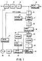
- Fig. 1 is a block diagram showing the structure of a demodulator according to an embodiment of the present invention.
- Fig. 2 is a diagram illustrating the operation of the demodulator according to the embodiment shown in Fig. 1.
- Fig. 3 is a block diagram showing the structure of a demodulator according to a modification of the embodiment shown in Fig. 1.
- Fig. 4 is a block diagram showing the structure of a conventional demodulator.
- Figs. 1 and 2 are a block diagram showing the structure of a demodulator according to an embodiment of the invention, and a diagram illustrating the operation of the demodulator.
- the demodulator of this embodiment will be described, taking as an example a receiver for receiving radio waves of digital-audio broadcasting in conformity with European Broadcasting Union.
- a received intermediate frequency signal which was OFDM modulated is supplied to an input terminal and A/D converted by an A/D converter 1.
- the A/D converted signal is converted into parallel data by a serial/parallel converter 2.
- This parallel data is supplied to an FFT circuit 3 whereat it is Fourier transformed to be converted from signals in a time domain into signals in a frequency domain.
- An output of the FFT circuit 3 is delay-detected by a delay detector 4 and output as a demodulated signal.
- An output from the FFT circuit 3 is also supplied to a switch circuit 5 which is controlled by a gate signal from a timing generator 17.
- the switch circuit 5 passes only a PRS of the output from the FFT circuit 3.
- a pattern generator 6 generates a carrier in accordance with a conjugate complex number signal of a signal in the frequency range represented by the PRS symbol.
- the carrier generated by the pattern generator 6 in accordance with the conjugate complex number signal and a carrier received from the PRS symbol are multiplied together by a cross power calculator 7 to obtain a cross power.
- the calculation results of the cross power calculator 7 indicate a frequency transfer function of the transmission path at the frequency point where the carrier is present.
- each carrier is given by the following equation (3).
- the pattern generator 6 generates each carrier given by the following equation (5), each carrier being contained in the conjugate complex number signal of the PRS symbol given by the following equation (4).
- the cross power calculator 7 calculates the cross power of the carrier based on the received PRS symbol given by the equation (3) and the carrier given by the equation (5). Therefore, the cross power calculator 7 outputs a signal Ck (-768 ⁇ k ⁇ 768, k is not 0), and the frequency transfer function at the point where the carrier is present can be known.
- An output signal of the cross power calculator 7 is inverse Fourier transformed by an IFFT circuit 8.
- the frequency transfer function can be obtained by FFT-ing the impulse response signal, and a complex impulse response signal can be obtained by IFFT-ing the frequency transfer function. Therefore, with the inverse Fourier transformation, the IFFT circuit 8 can output a pseudo complex impulse response signal of the transmission path.
- the complex impulse response signal output from the IFFT circuit 8 is supplied to a power calculation circuit 9 which performs a square calculation of the input complex impulse response signal to obtain a power signal, i.e., an impulse response signal.
- the power signal output, i.e., impulse response signal output from the power calculation circuit 9 is supplied to a data shift circuit 10 and a window circuit 18.
- the data shift circuit 10 Upon reception of the power signal output, i.e., impulse response signal, the data shift circuit 10 shifts the data order of the impulse response signal in accordance with a control signal supplied from a peak position detector 13 to be described later.
- the shifted impulse response signal is supplied to a window circuit 11 having a time duration nearly equal to a guard interval period.
- the impulse response signal having a sequentially shifted data order is picked up during a time period (hereinafter called a guard interval time window) generally equal to a guard interval period, and supplied to an adder 12 which calculates a sum of input impulse response signal levels, i.e., a total power and sends it to the peak position detector 13.
- a guard interval time window a time period
- an adder 12 which calculates a sum of input impulse response signal levels, i.e., a total power and sends it to the peak position detector 13.
- the peak position detector 13 detects the position of a peak value of the total power, and sends it to a timing control circuit 14.
- the timing control circuit 14 controls via a D/A converter 15 the oscillation frequency of a VCXO 16. With the controlled oscillation signal of VCXO 16, a sampling clock signal of the A/D converter 1 to be output from the timing generator 17 and the gate signal for controlling the switch circuit 5 are controlled.
- the window circuit 18 picks up only the signal in the time duration during which symbol interference may occur, and sends it to a level detector 19. If data input to the level detector 19 contains data of a predetermined level or higher, the level detector 19 controls the timing controller 14 so that the gain thereof is increased.
- the impulse response signal as indicated at (d) in Fig. 2 is picked up during the time duration corresponding to the guard interval time window nearly equal to the guard interval period, and the adder calculates its total power.
- the adder 12 repeats the addition calculation to obtain the total power in the guard interval time window as indicated at (e) in Fig. 2.
- An FFT window for Fourier transformation by the FFT circuit 3 is indicated at (c) in Fig. 2.
- the peak position detector 13 Upon reception of the addition results, i.e., total power from the adder 12, the peak position detector 13 obtains the peak position of a total power.
- the timing control circuit 14 controls the oscillation frequency of the D/A converter 15 via VCXO 16 so that the reception timing is adjusted with the peak position being converged into a target position. Therefore, the phase of a sampling clock signal of the A/D converter 1 output from the timing generator 17 is shifted to obtain the target position, i.e., optimum reception timing.
- the switch circuit 5 is controlled by the gate signal output from the timing generator 17 to pick up the PRS symbol.
- the window circuit 18 picks up the power of the impulse response signal corresponding only to the signal received from the transmission path during the period symbol interference may occur, and if the power has a predetermined level or higher, it is detected by the level detector 19.
- the gain of the timing controller 14 is increased to improve the response characteristics of reception timing control. Accordingly, the tracking characteristics against abrupt changes in all transmission paths can be improved, and stability in a steady state is ensured.
- the time length of the guard interval time window is set generally equal to the guard interval period, because it is determined based upon the period during which reproduced sounds may be affected by multipath or the like.
- the time length of the guard interval time window of the window circuit 11 may be changed in accordance with the response characteristics of reception timing control and some allowance of the change in transmission paths.
- FIG. 3 is a block diagram showing the structure of a modification of the demodulator of the above embodiment.
- the window circuits 11 and 18, adder 12, peak position detector 13 and level detector 19 of the above embodiment are omitted.
- the data of an impulse response signal is shifted by the data shift circuit 10, the shifted output signal is supplied to a symbol interference calculator 20 to calculate symbol interference.
- the symbol interference calculator 20 calculates a total interference level in accordance with the power level of all signals received from transmission paths on which symbol interference may occur, i.e., in accordance with a shift between the level and timing of an OFDM symbol. This calculation is repeated while the data shift circuit 10 shifts the data of the impulse response signal.
- the oscillation frequency of VCXO 16 is controlled by the timing controller 14 to make the interference level lowest.
- the phase of the sampling clock signal of the A/D converter 1 output from the timing generator 17 which is controlled by the oscillation frequency of VCXO 16 can be controlled, and the reception timing is controlled to make symbol interference lowest in any reception environment including such a case wherein signals received from transmission paths are not in the time period of the guard interval.
- the window circuit 18 and level detector 19 of the demodulator of the embodiment shown in Fig. 1 may be used to increase the gain of the timing controller 14 during symbol interference.
- the demodulator of this invention can receive radio waves at a timing with less symbol interference when a plurality of radio waves are received with a single antenna in an SFN environment or in a multipath environment.
Landscapes
- Engineering & Computer Science (AREA)
- Computer Networks & Wireless Communication (AREA)
- Signal Processing (AREA)
- Noise Elimination (AREA)
- Synchronisation In Digital Transmission Systems (AREA)
- Cable Transmission Systems, Equalization Of Radio And Reduction Of Echo (AREA)
Applications Claiming Priority (3)
| Application Number | Priority Date | Filing Date | Title |
|---|---|---|---|
| JP309909/96 | 1996-11-07 | ||
| JP30990996A JP3453696B2 (ja) | 1996-11-07 | 1996-11-07 | 復調器 |
| JP30990996 | 1996-11-07 |
Publications (2)
| Publication Number | Publication Date |
|---|---|
| EP0841787A2 true EP0841787A2 (fr) | 1998-05-13 |
| EP0841787A3 EP0841787A3 (fr) | 2001-06-27 |
Family
ID=17998804
Family Applications (1)
| Application Number | Title | Priority Date | Filing Date |
|---|---|---|---|
| EP97118177A Withdrawn EP0841787A3 (fr) | 1996-11-07 | 1997-10-20 | Synchronisation dans un récepteur multiporteur |
Country Status (3)
| Country | Link |
|---|---|
| EP (1) | EP0841787A3 (fr) |
| JP (1) | JP3453696B2 (fr) |
| DE (1) | DE841787T1 (fr) |
Cited By (3)
| Publication number | Priority date | Publication date | Assignee | Title |
|---|---|---|---|---|
| WO2001069878A1 (fr) * | 2000-03-15 | 2001-09-20 | Conexant Digital Infotainment Limited | Procede de selection d'une position d'une fenetre tfr dans un recepteur cofdm |
| EP0963068A3 (fr) * | 1998-06-02 | 2001-11-28 | Mitsubishi Denki Kabushiki Kaisha | Récepteur pour la réception de programmes radiophoniques numériques utilisant l'addition pondérée des données de réponse impulsionelle d'un canal pour adapter la fenêtre d'échantillonage |
| GB2525459A (en) * | 2014-10-22 | 2015-10-28 | Imagination Tech Ltd | Symbol boundary detection |
Families Citing this family (4)
| Publication number | Priority date | Publication date | Assignee | Title |
|---|---|---|---|---|
| JP4563620B2 (ja) * | 2001-07-18 | 2010-10-13 | 日本無線株式会社 | 伝送路特性測定装置 |
| GB2395094A (en) * | 2002-10-28 | 2004-05-12 | Sony Uk Ltd | Determining a symbol synch time in an OFDM receiver |
| US8144824B2 (en) * | 2005-03-10 | 2012-03-27 | Qualcomm Incorporated | Trend influenced time tracking |
| JP5307797B2 (ja) * | 2008-03-31 | 2013-10-02 | パナソニック株式会社 | 受信装置、受信方法、受信プログラム、集積回路及びデジタルテレビ |
Family Cites Families (2)
| Publication number | Priority date | Publication date | Assignee | Title |
|---|---|---|---|---|
| JP3485117B2 (ja) * | 1993-09-10 | 2004-01-13 | ドイチェ トムソン−ブラント ゲーエムベーハー | Ofdm方式の基準信号の伝送方法 |
| FR2743967B1 (fr) * | 1996-01-18 | 1998-03-27 | France Telecom | Procede et dispositif de synchronisation temporelle d'un recepteur d'un signal multiporteuse |
-
1996
- 1996-11-07 JP JP30990996A patent/JP3453696B2/ja not_active Expired - Lifetime
-
1997
- 1997-10-20 DE DE1997118177 patent/DE841787T1/de active Pending
- 1997-10-20 EP EP97118177A patent/EP0841787A3/fr not_active Withdrawn
Non-Patent Citations (1)
| Title |
|---|
| None |
Cited By (6)
| Publication number | Priority date | Publication date | Assignee | Title |
|---|---|---|---|---|
| EP0963068A3 (fr) * | 1998-06-02 | 2001-11-28 | Mitsubishi Denki Kabushiki Kaisha | Récepteur pour la réception de programmes radiophoniques numériques utilisant l'addition pondérée des données de réponse impulsionelle d'un canal pour adapter la fenêtre d'échantillonage |
| US6434205B1 (en) | 1998-06-02 | 2002-08-13 | Mitsubishi Denki Kabushiki Kaisha | Digital broadcast receiver using weighted sum of channel impulse response data to adjust sampling window |
| WO2001069878A1 (fr) * | 2000-03-15 | 2001-09-20 | Conexant Digital Infotainment Limited | Procede de selection d'une position d'une fenetre tfr dans un recepteur cofdm |
| GB2525459A (en) * | 2014-10-22 | 2015-10-28 | Imagination Tech Ltd | Symbol boundary detection |
| GB2525459B (en) * | 2014-10-22 | 2017-01-11 | Imagination Tech Ltd | Symbol boundary detection |
| US9749124B2 (en) | 2014-10-22 | 2017-08-29 | Imagination Technologies Limited | Symbol boundary detection |
Also Published As
| Publication number | Publication date |
|---|---|
| EP0841787A3 (fr) | 2001-06-27 |
| JP3453696B2 (ja) | 2003-10-06 |
| JPH10145323A (ja) | 1998-05-29 |
| DE841787T1 (de) | 1998-09-24 |
Similar Documents
| Publication | Publication Date | Title |
|---|---|---|
| US6314083B1 (en) | Frequency control device and method for frequency synchronization with multiplex signal by OFDM, receiving device, and communication device | |
| EP0901259B1 (fr) | Corrections de décalages de phase et/ou de fréquence dans des signaux multiporteurs | |
| EP0712555B1 (fr) | Procede et appareil de synchronisation dans des systemes de transmission numerique a multiplexage par repartition orthogonale de la frequence | |
| EP1041736B1 (fr) | Récepteur en diversité pour la transmission de signaux en rafale | |
| US6246735B1 (en) | Synchronization detection method for data transmission apparatus and data transmission apparatus using the same | |
| US6711123B1 (en) | Receiving apparatus for OFDM communication system | |
| JP3846546B2 (ja) | 周波数オフセット推定器 | |
| EP0963086A2 (fr) | Dispositif de correction d'erreurs pour le traitement de bruit sélectif en fréquence | |
| RU2216113C2 (ru) | Приемник сигнала для цифрового звукового вещания | |
| EP0881705A2 (fr) | Récepteur à réseau d'antennes et procédé de correction de la quantité de décalage de phase de signal de réception | |
| EP0841787A2 (fr) | Synchronisation dans un récepteur multiporteur | |
| US7944996B2 (en) | OFDM reception device and OFDM receiver using the same | |
| JP2003051768A (ja) | ダイバーシティ受信機 | |
| EP0984562B1 (fr) | Détection synchrone par interpolation de pilote dans un récepteur du type Rake | |
| US6836518B1 (en) | Synchronization control method for receiver apparatus of data transmission system utilizing orthogonal frequency division multiplex, and data transmission system | |
| JP4309537B2 (ja) | Ofdm受信装置 | |
| US7415081B2 (en) | Orthogonal frequency division multiple signal reception apparatus, reception apparatus, orthogonal frequency division multiple signal reception method, and reception method | |
| US9444671B2 (en) | Antenna direction adjustment method and OFDM reception device | |
| EP1006699A2 (fr) | Synchronisation de symboles pour transmission multiporteuse | |
| EP1093268B1 (fr) | Dispositif de réception OFDM | |
| JP3649560B2 (ja) | 直交周波数分割多重信号発生装置および方法、復調装置、通信装置、直交周波数分割多重信号発生プログラムが格納された記憶媒体および復調プログラムが格納された記憶媒体 | |
| JP3944422B2 (ja) | ダイバーシティ受信機 | |
| JPH07154129A (ja) | Lms方式のアダプティブアレイアンテナ装置 | |
| KR20040023440A (ko) | 이동통신시스템의 수신단에서의 주파수 오차 추정 및 결합기 | |
| JP3767690B2 (ja) | ダイバーシティ受信機 |
Legal Events
| Date | Code | Title | Description |
|---|---|---|---|
| PUAI | Public reference made under article 153(3) epc to a published international application that has entered the european phase |
Free format text: ORIGINAL CODE: 0009012 |
|
| AK | Designated contracting states |
Kind code of ref document: A2 Designated state(s): DE FR GB |
|
| AX | Request for extension of the european patent |
Free format text: AL;LT;LV;RO;SI |
|
| EL | Fr: translation of claims filed | ||
| DET | De: translation of patent claims | ||
| PUAL | Search report despatched |
Free format text: ORIGINAL CODE: 0009013 |
|
| AK | Designated contracting states |
Kind code of ref document: A3 Designated state(s): AT BE CH DE DK ES FI FR GB GR IE IT LI LU MC NL PT SE |
|
| AX | Request for extension of the european patent |
Free format text: AL;LT;LV;RO;SI |
|
| 17P | Request for examination filed |
Effective date: 20011213 |
|
| AKX | Designation fees paid |
Free format text: DE FR GB |
|
| APBN | Date of receipt of notice of appeal recorded |
Free format text: ORIGINAL CODE: EPIDOSNNOA2E |
|
| APBR | Date of receipt of statement of grounds of appeal recorded |
Free format text: ORIGINAL CODE: EPIDOSNNOA3E |
|
| APAF | Appeal reference modified |
Free format text: ORIGINAL CODE: EPIDOSCREFNE |
|
| APAF | Appeal reference modified |
Free format text: ORIGINAL CODE: EPIDOSCREFNE |
|
| RAP1 | Party data changed (applicant data changed or rights of an application transferred) |
Owner name: KABUSHIKI KAISHA KENWOOD |
|
| APBT | Appeal procedure closed |
Free format text: ORIGINAL CODE: EPIDOSNNOA9E |
|
| RAP1 | Party data changed (applicant data changed or rights of an application transferred) |
Owner name: JVC KENWOOD CORPORATION |
|
| STAA | Information on the status of an ep patent application or granted ep patent |
Free format text: STATUS: THE APPLICATION HAS BEEN WITHDRAWN |
|
| 18W | Application withdrawn |
Effective date: 20130718 |