EP0881705A2 - Récepteur à réseau d'antennes et procédé de correction de la quantité de décalage de phase de signal de réception - Google Patents
Récepteur à réseau d'antennes et procédé de correction de la quantité de décalage de phase de signal de réception Download PDFInfo
- Publication number
- EP0881705A2 EP0881705A2 EP98109898A EP98109898A EP0881705A2 EP 0881705 A2 EP0881705 A2 EP 0881705A2 EP 98109898 A EP98109898 A EP 98109898A EP 98109898 A EP98109898 A EP 98109898A EP 0881705 A2 EP0881705 A2 EP 0881705A2
- Authority
- EP
- European Patent Office
- Prior art keywords
- phase shift
- receiving
- shift amount
- phase
- phase control
- Prior art date
- Legal status (The legal status is an assumption and is not a legal conclusion. Google has not performed a legal analysis and makes no representation as to the accuracy of the status listed.)
- Withdrawn
Links
Images


Classifications
-
- H—ELECTRICITY
- H01—ELECTRIC ELEMENTS
- H01Q—ANTENNAS, i.e. RADIO AERIALS
- H01Q3/00—Arrangements for changing or varying the orientation or the shape of the directional pattern of the waves radiated from an antenna or antenna system
- H01Q3/26—Arrangements for changing or varying the orientation or the shape of the directional pattern of the waves radiated from an antenna or antenna system varying the relative phase or relative amplitude of energisation between two or more active radiating elements; varying the distribution of energy across a radiating aperture
- H01Q3/2605—Array of radiating elements provided with a feedback control over the element weights, e.g. adaptive arrays
-
- H—ELECTRICITY
- H01—ELECTRIC ELEMENTS
- H01Q—ANTENNAS, i.e. RADIO AERIALS
- H01Q3/00—Arrangements for changing or varying the orientation or the shape of the directional pattern of the waves radiated from an antenna or antenna system
- H01Q3/26—Arrangements for changing or varying the orientation or the shape of the directional pattern of the waves radiated from an antenna or antenna system varying the relative phase or relative amplitude of energisation between two or more active radiating elements; varying the distribution of energy across a radiating aperture
Definitions
- the present invention relates to an antenna array receiver for performing reception by use of an antenna array.
- the present invention also relates to a method of correcting a phase shift amount of a receiving signal.
- a receiver in order to perform directional reception by use of an antenna array, a receiver is designed so as to perform reception while maintaining the phase difference at the antenna terminals among receiving signals from a plurality of antennas.
- FIG. 1 shows an example of the antenna array receiver.
- receiving signals S1 and S2 at antennas 1301 and 1302 are amplified by receiving amplifiers 1303 and 1304. Then, the signals are multiplied by a signal from an oscillator 1307 by mixers 1305 and 1306 and a lower-frequency signal is extracted by band-pass filters (BPFs) 1308 and 1309.
- BPFs band-pass filters
- quadrature demodulators 1310 and 1311 quadrature demodulation is performed by use of a signal from an oscillator 1312, and in-phase components S11 and S21 and quadrature components S12 and S22 are output. These output signals are converted into digital values by A/D converters 1313, 1314, 1315 and 1316, and output to an adaptive antenna array receiving circuit 1317.
- the lower-frequency signal extracted by the BPFs 1308 and 1309 is monitored and the levels of the receiving signals are detected.
- the gains of the receiving amplifiers 1303 and 1304 are controlled by gain control circuits 1320 and 1321.
- the levels of receiving signals vary with time. Particularly, in a mobile communication environment, the levels of receiving signals largely vary in a short period of time due to fading, variation in propagated distance and shadowing because of buildings and the like.
- the receiving signal levels are corrected to thereby optimize the input to the A/D converter.
- the phase shift amount of a receiving amplifier varies according to the gain thereof.
- the amount of the phase variation differs among receiving amplifiers.
- the phase shift amount varies according to the frequency and the temperature of the receiving amplifier.
- the electric length i.e. the length converted into a wavelength, varies according to the frequency.
- One object of the present invention is to provide an antenna array receiver in which receiving signals can be input to a receiving circuit with the phase difference at the antenna terminals between the receiving signals of the antennas being maintained.
- Another object of the present invention is to provide a method of correcting phase shift amounts of receiving signals in which the receiving signals can be input to a receiving circuit with the phase difference at the antenna terminals between the receiving signals of the antennas being maintained.
- the present invention provides an antenna array receiver comprising:
- the present invention provides a method of correcting a phase shift amount of a receiving signal, comprising the steps of:
- the present invention provides an antenna array receiver comprising:
- the present invention provides an antenna array receiver comprising:
- the present invention provides a method of correcting a phase shift amount of a receiving signal, comprising the steps of:
- FIG. 2 is a block diagram showing an antenna array receiver according to a first embodiment of the present invention. While the number of antennas is two for ease of explanation, the basic operation is the same when the number of antennas is more than three.
- receiving signals S1 and S2 at first and second antennas 101 and 102 are amplified by receiving amplifiers 103 and 104. Then, the signals are multiplied by a signal from an oscillator 107 by mixers 105 and 106 and a lower-frequency signal is extracted by band-pass filters (hereinafter, referred to as BPFs) 108 and 109.
- BPFs band-pass filters
- quadrature demodulators 110 and 111 quadrature demodulation is performed by use of a signal from an oscillator 112, and in-phase components S11 and S21 and quadrature components S21 and S22 are output. These output signals are converted into digital values by A/D converters 113, 114, 115 and 116. The results are input to vector multiply circuits 117 and 118.
- the vector multiply circuits 117 and 118 shift the phases of input signals S13, S14, S23 and S24 in accordance with control signals SC1 and SC2 from phase control amount tables 119 and 120 and outputs the phase-shifted signals to an adaptive antenna array receiving circuit 121.
- the lower-frequency signal extracted by the BPFs 108 and 109 is monitored and the levels of the receiving signals are detected.
- the gains of the receiving amplifiers 103 and 104 are controlled by gain control circuits 124 and 125.
- the gain control signals are simultaneously converted into digital values by A/D converters 126 and 127 and input to the first and second phase control amount tables (referred to as First table and Second table in the figures) 119 and 120, respectively.
- phase control signals Sc1 and Sc2 are output to the vector multiply circuits 117 and 118.
- the phase control signals Sc1 and Sc2 represent phase shift amounts corresponding to the gains represented by gain control signals Sg1 and Sg2 as arguments.
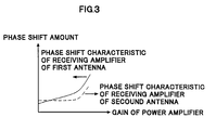
- FIG. 3 is a view showing the gain versus phase shift amount characteristics of the receiving amplifiers.
- the solid line represents the gain versus phase shift amount characteristic of the receiving amplifier of the first antenna 101.
- the broken line represents the gain versus phase shift amount characteristic of the receiving amplifier of the second antenna 102.
- phase control amount tables 119 and 120 the characteristics are stored with the gains as the arguments. Since there are n receiving amplifiers when there are n antennas in practice, the characteristic of each amplifier is previously measured and stored in the table.
- the amount of phase shift cause mainly by the receiving amplifier in each antenna are corrected in correspondence with the gain control amount responsive to the receiving signal level. Therefore, the receiving signals can be input to the adaptive antenna array receiving circuit 121 with the phase difference at the antenna terminals being maintained.
- the determined phase shift control amount may be corrected.
- (d-b) is obtained by comparing a receiving signal a x exp(jb) at the end part of the channel at the first and second antennas 101 and 102 side with a receiving signal c x exp(jb) before the A/D converters 113 through 116.
- This value of (d-b) is a phase shift amount from the first antennas 101 and 102 to the A/D converters 113, 114, 115 and 116. Therefore, the phase shift control amount determined above is corrected on the basis of the value of (d-b).
- FIG. 4 is a block diagram showing a relevant part of an antenna array receiver according to a second embodiment of the present invention.
- the antenna terminals and the receiving RF portion are omitted from the block of the antenna array receiver shown in FIG. 2.
- phase shift amounts of the receiving amplifiers vary also according to the frequency. Therefore, in the second embodiment, the correction of the phase shift amount is performed also with respect to the frequency in use.
- the gain versus phase shift amount characteristic of each of the receiving amplifiers of the first and second antennas 101 and 102 is measured with respect to each of frequencies f1 and f2 in use, and the measured characteristics are stored in first and second phase control amount tables 319 and 320. Consequently, in the first phase control amount table 319, the gain versus phase shift amount characteristic of the receiving amplifier of the first antenna 101 is stored. Also, in the second phase control amount table, the gain versus phase shift amount characteristic of the receiving amplifier of the second antenna 102 is stored.
- the gain control signals Sg1 and Sg2 of the receiving amplifiers and a frequency-in-use signal Sf are input to the phase control amount tables 319 and 320 to obtain the phase control signals Sc1 and Sc2 representative of phase shift amounts.
- the phases of the in-phase components S13 and S23 and the quadrature components S14 and S24 of the first and second antennas 101 and 102 are shifted in opposite directions in accordance with the phase control signals Sc1 and Sc2.
- signals can be input to an adaptive antenna array receiving circuit 321 with the phase difference at the antenna terminals being maintained with respect to all the frequencies in use.
- the determined phase shift control amount may be corrected on the basis of the difference of phase shift amount produced by the difference of channel length.
- FIG. 6 is a block diagram showing a relevant part of an antenna array receiver according to a third embodiment of the present invention. Like in the second embodiment, the antenna terminals and the receiving RF portion are omitted for ease of explanation.
- the phase shift amount is controlled in consideration of the operating temperatures of the receiving amplifiers.
- the transmit RF portion is high in temperature because the power consumption is great. Since the phase shift amount sometimes varies according to the temperature in some receiving amplifiers, it is desirable to perform the correction of the phase shift amount with respect to the temperature variation of the receiving amplifiers by use of the gain versus phase shift amount characteristic table for each temperature.
- the gain versus phase shift amount characteristic of each of the receiving amplifiers of the first and second antennas 101 and 102 is measured with respect to each of operating temperatures T1 and T2, and the measured characteristics are stored in first and second phase control amount tables 519 and 520.
- the gain control signals Sg1 and Sg2 of the receiving amplifiers and operating temperature signals St1 and St2 are input to the phase control amount tables 519 and 520 to obtain the phase control signals Sc1 and Sc2 representative of phase shift amounts.
- the phases of the in-phase components S13 and S23 and the quadrature components S14 and S24 of the first and second antennas 101 and 102 are shifted in opposite directions in accordance with the phase control signals Sc1 and Sc2.
- signals can be input to an adaptive antenna array receiving circuit 521 with the phase difference at the antenna terminals being maintained with respect to all the temperatures.
- the determined phase shift control amount may be corrected on the basis of the difference of phase shift amount produced by the difference of channel length.
- FIG. 8 is a block diagram showing a relevant part of an antenna array receiver according to a fourth embodiment of the present invention. Like in the third embodiment, the antenna terminals and the receiving RF portion are omitted for ease of explanation.
- the correction of the phase shift amount is performed in consideration of both the frequency and the temperature in use by use of a table of the gain versus phase shift amount characteristic for each of the frequency and the temperature in use.
- the gain versus phase shift amount characteristic is measured with respect to each frequency in use and each temperature. For example, as shown in FIGs. 9A and 9B, four kinds of gain versus phase shift amount characteristics are measured with combinations of two kinds of frequencies (f1 and f2) and two kinds of temperatures (T1 and T2), and the characteristics of the receiving amplifiers 103 and 104 of the antennas 101 and 102 are stored in first and second phase control amount tables 719 and 720.
- the gain signals Sg1 and Sg2 of the receiving amplifiers 103 and 104, the frequency-in-use signal Sf and the operating temperature signals St1 and St2 are input to the phase control amount tables 719 and 720 to obtain the phase control signals Sc1 and Sc2 representative of phase shift amounts.
- the phases of the in-phase components S13 and S23 and the quadrature components S14 and S24 of the antennas 101 and 102 are shifted in opposite directions in accordance with the phase control signals Sc1 and Sc2.
- signals can be input to an adaptive antenna array receiving circuit 721 with the phase difference at the antenna terminals being maintained with respect to all the frequencies and temperatures in use.
- the determined phase shift control amount may be corrected on the basis of the difference of phase shift amount produced by the difference of channel length.
- FIG. 10 is a block diagram showing a relevant part of an antenna array receiver according to a fifth embodiment of the present invention. Like in the fourth embodiment, the antenna terminals and the receiving RF portion are omitted for ease of explanation.
- the phase shift amount for a necessary gain is calculated through interpolation.
- phase shift amount aij (i represents a frequency number and j represents a temperature number) for a gain G1
- a phase shift amount bij for a gain G2 and a phase shift amount cij for a gain G3 are measured
- the characteristic of the receiving amplifier 103 and the characteristic of the receiving amplifier 104 are stored in phase control amount tables 919 and 920, respectively.
- the frequency-in-use signal Sf and the temperature St1 are input to the first phase control amount table 919 as the arguments to obtain a phase shift amount vector (aij, bij and cij).
- a signal Sr1 representative of the phase shift amount vector and the gain signal Sg1 of the receiving amplifier are input to an interpolate circuit 930, and the phase control signal Sc1 corresponding to the gain signal Sr1 of the receiving amplifier is calculated.
- the phases of the in-phase component S13 and the quadrature component S14 of the first antenna 101 are shifted in opposite directions by use of the phase control signal Sc1.
- the frequency-in-use signal Sf and the temperature St2 are input to the second phase control amount table 920 as the arguments to obtain a phase shift amount vector (aij, bij and cij).
- a signal Sr2 representative of the phase shift amount vector and the gain signal Sg2 of the receiving amplifier are input to an interpolate circuit 931 and the phase control signal Sc2 corresponding to the gain signal Sg2 of the receiving amplifier is calculated.
- the phases of the in-phase component S23 and the quadrature component S24 of the second antenna 102 are shifted in opposite directions by use of the phase control signal Sc2.
- signals can be input to an adaptive antenna array receiving circuit 921 with the phase difference at the antenna terminals being maintained with respect to all the frequencies in use and temperatures with a small memory amount.
- FIG. 13 is a block diagram showing an antenna array receiver according to a sixth embodiment of the present invention. Like in the fifth embodiment, the antenna terminals and the receiving RF portion are omitted for ease of explanation.
- AFC automatic frequency control
- the gain Sg1 of the receiving amplifier of the signal processing system of the first antenna is input to a phase control amount table 1219, and the signal Sr1 representative of the phase shift amount vector is set to a frequency offset control circuit 1232.
- a frequency offset correction table 1234 is searched by use of a frequency offset signal So and the signal Sr1, and the phase control signal Sc1 corresponding to a frequency offset correction value Soc1 is output.
- the phases of the in-phase component S13 and the quadrature component S14 of the first antenna are shifted in opposite directions in accordance with the phase control signal Sc1.
- the gain Sg2 of the receiving amplifier of the signal processing system of the second antenna is input to a phase control amount table 1220, and the signal Sr2 representative of the phase shift amount vector is set to a frequency offset control circuit 1233.
- a frequency offset correction table 1234 is searched by use of a frequency offset signal So and the signal Sr2, and the phase control signal Sc2 corresponding to a frequency offset correction value Soc1 is output.
- the phases of the in-phase component S23 and the quadrature component S24 of the second antenna are shifted in opposite directions in accordance with the phase control signal Sc2.
- frequency offset signal So is obtained by a frequency offset detecting circuit 1240 which carries out the following calculations.
- a transmission signal tx(kT) a(kT) x exp(i ⁇ (kT)) is transmitted.
- symbol time interval is T.
- a receiving signal is as shown in the following equation.
- rx(kT) b(kT) x exp(i ⁇ (kT)) x exp(j(k ⁇ + ⁇ )) wherein a(kT) is an amplitude of time kT, ⁇ (kT) is a phase of time kT, b(kT) is an amplitude fluctuation on the line, ⁇ is a phase change amount in time T interval, and ⁇ is the initial phase of a receiver.
- the frequency offset component ⁇ at one symbol time interval is calculated.
- phase shift amount integration value (n ⁇ + ⁇ 1 where ⁇ is the phase shift amount and n is a symbol number) is calculated every symbol time based on the frequency offset per symbol time.
- sin((n ⁇ + ⁇ 1)%2 ⁇ ) and cos((n ⁇ + ⁇ 1)%2 ⁇ ) corresponding to the phase shift amount integration value are detected through the search of the table.
- the output result is the frequency offset correction value Soc1 and is output to the vector multiply circuit as the phase control signal Sc1.
- % is a modulo arithmetic. While sin((n ⁇ + ⁇ 1)%2 ⁇ ) and cos((n ⁇ + ⁇ 1)%2 ⁇ ) are calculated with reference to the frequency offset correction table in FIG. 13, they may be directly calculated by use of an approximate expression and the like without the use of the table.
- the two vector multiply circuits namely the vector multiply circuit for the phase shift amount correction and the vector multiply circuit for the AFC processing can be reduced to one.
- the phase shift amount correction table may be provided for the frequency, for the temperature and for both the frequency and the temperature.
- the phase shift amount for the gain may be roughly set in advance so that the phase shift amount for a desired gain is calculated through interpolation processing based on the previously obtained value.
- the two vector multiply circuits namely the vector multiply circuit for the phase shift amount correction and the vector multiply circuit for the AFC processing can be reduced to one.
- the antenna array receiver of the present invention described above is applicable to receivers for base stations and for mobile stations.
Landscapes
- Variable-Direction Aerials And Aerial Arrays (AREA)
- Radio Transmission System (AREA)
Applications Claiming Priority (3)
| Application Number | Priority Date | Filing Date | Title |
|---|---|---|---|
| JP158126/97 | 1997-05-30 | ||
| JP15812697 | 1997-05-30 | ||
| JP15812697 | 1997-05-30 |
Publications (2)
| Publication Number | Publication Date |
|---|---|
| EP0881705A2 true EP0881705A2 (fr) | 1998-12-02 |
| EP0881705A3 EP0881705A3 (fr) | 2000-12-06 |
Family
ID=15664866
Family Applications (1)
| Application Number | Title | Priority Date | Filing Date |
|---|---|---|---|
| EP98109898A Withdrawn EP0881705A3 (fr) | 1997-05-30 | 1998-05-29 | Récepteur à réseau d'antennes et procédé de correction de la quantité de décalage de phase de signal de réception |
Country Status (4)
| Country | Link |
|---|---|
| US (1) | US5933112A (fr) |
| EP (1) | EP0881705A3 (fr) |
| KR (1) | KR100282384B1 (fr) |
| CN (1) | CN1096757C (fr) |
Cited By (2)
| Publication number | Priority date | Publication date | Assignee | Title |
|---|---|---|---|---|
| GB2360635A (en) * | 1998-02-24 | 2001-09-26 | Univ Belfast | Retroreceive antenna |
| US7020492B2 (en) | 2000-04-03 | 2006-03-28 | Sanyo Electric Co., Ltd. | Radio |
Families Citing this family (16)
| Publication number | Priority date | Publication date | Assignee | Title |
|---|---|---|---|---|
| US6628630B1 (en) | 1997-04-15 | 2003-09-30 | Matsushita Electric Industrial Co., Ltd. | Spread spectrum communication method |
| JP2000091833A (ja) * | 1998-09-14 | 2000-03-31 | Fujitsu Ltd | アレーアンテナ受信装置 |
| SE513136C2 (sv) * | 1998-11-20 | 2000-07-10 | Ericsson Telefon Ab L M | Förfarande och anordning vid radiokommunikation |
| US6400318B1 (en) * | 1999-04-30 | 2002-06-04 | Kabushiki Kaisha Toshiba | Adaptive array antenna |
| US7233627B2 (en) * | 2000-02-23 | 2007-06-19 | Ipr Licensing, Inc. | Method for searching pilot signals to synchronize a CDMA receiver with an associated transmitter |
| JP4318389B2 (ja) * | 2000-04-03 | 2009-08-19 | 三洋電機株式会社 | アダプティブアレー装置、無線基地局、携帯電話機 |
| DE10025837A1 (de) * | 2000-05-25 | 2001-12-13 | Rohde & Schwarz | Breitbandempfänger |
| EP1220475A3 (fr) * | 2000-12-25 | 2003-11-19 | Kabushiki Kaisha Toshiba | Appareil mobile terminal avec un réseau d'antennes |
| JP2002290254A (ja) * | 2001-03-26 | 2002-10-04 | Nec Corp | ダイレクトコンバージョン受信機 |
| US7139533B2 (en) * | 2002-09-24 | 2006-11-21 | Hitachi, Ltd. | Mobile communication terminal |
| DE10311836B4 (de) * | 2003-03-18 | 2006-10-05 | Integrated Electronic Systems !Sys Consulting Gmbh | Ferngesteuertes Industriegerät |
| US20060183451A1 (en) * | 2003-06-06 | 2006-08-17 | Interdigital Technology Corporation | Method and system for continuously compensating for phase variations introduced into a communication signal by automatic gain control adjustments |
| US8953663B2 (en) * | 2009-09-25 | 2015-02-10 | Intel Corporation | Calibration of quadrature imbalance via loopback phase shifts |
| US8711905B2 (en) | 2010-05-27 | 2014-04-29 | Intel Corporation | Calibration of quadrature imbalances using wideband signals |
| WO2012124009A1 (fr) | 2011-03-17 | 2012-09-20 | 三菱電機株式会社 | Dispositif de détection de l'inclinaison d'un véhicule |
| CN110927751B (zh) * | 2019-12-09 | 2022-05-17 | 中国电子科技集团公司第五十四研究所 | 一种基于载波相位测量的阵列天线自适应校正实现方法 |
Family Cites Families (5)
| Publication number | Priority date | Publication date | Assignee | Title |
|---|---|---|---|---|
| US5412414A (en) * | 1988-04-08 | 1995-05-02 | Martin Marietta Corporation | Self monitoring/calibrating phased array radar and an interchangeable, adjustable transmit/receive sub-assembly |
| EP0472621A4 (en) * | 1989-05-18 | 1992-08-05 | Motorola, Inc. | Method and apparatus for reducing intermodulation distortion |
| US5142695A (en) * | 1991-03-21 | 1992-08-25 | Novatel Communications, Ltd. | Cellular radio-telephone receiver employing improved technique for generating an indication of received signal strength |
| US5722063A (en) * | 1994-12-16 | 1998-02-24 | Qualcomm Incorporated | Method and apparatus for increasing receiver immunity to interference |
| US5666124A (en) * | 1995-12-14 | 1997-09-09 | Loral Aerospace Corp. | High gain array antenna system |
-
1998
- 1998-05-21 US US09/082,461 patent/US5933112A/en not_active Expired - Lifetime
- 1998-05-29 CN CN98109502A patent/CN1096757C/zh not_active Expired - Fee Related
- 1998-05-29 EP EP98109898A patent/EP0881705A3/fr not_active Withdrawn
- 1998-05-30 KR KR1019980020128A patent/KR100282384B1/ko not_active Expired - Fee Related
Cited By (3)
| Publication number | Priority date | Publication date | Assignee | Title |
|---|---|---|---|---|
| GB2360635A (en) * | 1998-02-24 | 2001-09-26 | Univ Belfast | Retroreceive antenna |
| GB2360635B (en) * | 1998-02-24 | 2002-06-26 | Univ Belfast | Retroreceive antenna |
| US7020492B2 (en) | 2000-04-03 | 2006-03-28 | Sanyo Electric Co., Ltd. | Radio |
Also Published As
| Publication number | Publication date |
|---|---|
| KR19980087539A (ko) | 1998-12-05 |
| CN1096757C (zh) | 2002-12-18 |
| US5933112A (en) | 1999-08-03 |
| KR100282384B1 (ko) | 2001-02-15 |
| CN1201299A (zh) | 1998-12-09 |
| EP0881705A3 (fr) | 2000-12-06 |
Similar Documents
| Publication | Publication Date | Title |
|---|---|---|
| US5933112A (en) | Antenna array receiver and a method of correcting a phase shift amount of a receiving signal | |
| JP3709316B2 (ja) | 通信装置及び通信方法 | |
| US20020159118A1 (en) | Base station apparatus provided with array antennas | |
| US7929922B2 (en) | Radio communication system, a transmitter and a receiver | |
| JP3444270B2 (ja) | アレーアンテナ受信装置の校正システム | |
| EP0851605B1 (fr) | Circuit récepteur en diversité d'espace | |
| JP3369466B2 (ja) | アレーアンテナ無線受信装置のキャリブレーション装置 | |
| US8712356B2 (en) | Apparatus and method for phase synchronization in radio frequency transmitters | |
| US6708020B1 (en) | Calibration device | |
| US20080039024A1 (en) | Amplifying Circuit, Radio Communication Circuit, Radio Base Station Device and Radio Terminal Device | |
| US7054397B1 (en) | Mobile communication system having mobile stations and a base station | |
| US7924954B2 (en) | Frequency correction | |
| EP0984562B1 (fr) | Détection synchrone par interpolation de pilote dans un récepteur du type Rake | |
| US20090295636A1 (en) | Receiving Apparatus, Signal Processing Circuit, and Receiving System | |
| JP3589605B2 (ja) | 適応アレーアンテナ送受信装置 | |
| JP2000286629A (ja) | 無線送信装置及び送信指向性調整方法 | |
| JPH1146113A (ja) | アレーアンテナ受信装置及び受信信号の位相回転量補正方法 | |
| EP0841787A2 (fr) | Synchronisation dans un récepteur multiporteur | |
| KR101120545B1 (ko) | 다이버시티 수신기가 구비된 이동 무선 통신 디바이스, 및 안테나 수신 브랜치들을 통해 신호가 수신되는 방법 | |
| US20040166903A1 (en) | Base station | |
| JPH0365827A (ja) | ダイバーシチ受信回路 | |
| US8588350B2 (en) | Diversity receiver having cross coupled channel parameter estimation | |
| JP2792292B2 (ja) | 受信機 | |
| JP2008124534A (ja) | 指向性校正回路および指向性校正方法 |
Legal Events
| Date | Code | Title | Description |
|---|---|---|---|
| PUAI | Public reference made under article 153(3) epc to a published international application that has entered the european phase |
Free format text: ORIGINAL CODE: 0009012 |
|
| AK | Designated contracting states |
Kind code of ref document: A2 Designated state(s): DE FR GB |
|
| AX | Request for extension of the european patent |
Free format text: AL;LT;LV;MK;RO;SI |
|
| PUAL | Search report despatched |
Free format text: ORIGINAL CODE: 0009013 |
|
| AK | Designated contracting states |
Kind code of ref document: A3 Designated state(s): AT BE CH CY DE DK ES FI FR GB GR IE IT LI LU MC NL PT SE |
|
| AX | Request for extension of the european patent |
Free format text: AL;LT;LV;MK;RO;SI |
|
| RIC1 | Information provided on ipc code assigned before grant |
Free format text: 7H 01Q 3/26 A, 7H 04B 1/06 B, 7H 04B 7/005 B, 7H 03G 3/20 B |
|
| 17P | Request for examination filed |
Effective date: 20010116 |
|
| AKX | Designation fees paid |
Free format text: DE FR GB |
|
| 17Q | First examination report despatched |
Effective date: 20050405 |
|
| STAA | Information on the status of an ep patent application or granted ep patent |
Free format text: STATUS: THE APPLICATION IS DEEMED TO BE WITHDRAWN |
|
| 18D | Application deemed to be withdrawn |
Effective date: 20050817 |