EP0843191A1 - Mikrogeformter integrierter Keramiklichtreflektor - Google Patents
Mikrogeformter integrierter Keramiklichtreflektor Download PDFInfo
- Publication number
- EP0843191A1 EP0843191A1 EP97203384A EP97203384A EP0843191A1 EP 0843191 A1 EP0843191 A1 EP 0843191A1 EP 97203384 A EP97203384 A EP 97203384A EP 97203384 A EP97203384 A EP 97203384A EP 0843191 A1 EP0843191 A1 EP 0843191A1
- Authority
- EP
- European Patent Office
- Prior art keywords
- ceramic
- base element
- cavity
- light reflector
- green
- Prior art date
- Legal status (The legal status is an assumption and is not a legal conclusion. Google has not performed a legal analysis and makes no representation as to the accuracy of the status listed.)
- Withdrawn
Links
- 239000000919 ceramic Substances 0.000 title claims abstract description 89
- 238000000034 method Methods 0.000 claims abstract description 16
- 239000000843 powder Substances 0.000 claims description 31
- 239000004020 conductor Substances 0.000 claims description 19
- 238000005245 sintering Methods 0.000 claims description 17
- MCMNRKCIXSYSNV-UHFFFAOYSA-N Zirconium dioxide Chemical compound O=[Zr]=O MCMNRKCIXSYSNV-UHFFFAOYSA-N 0.000 claims description 16
- XUIMIQQOPSSXEZ-UHFFFAOYSA-N Silicon Chemical compound [Si] XUIMIQQOPSSXEZ-UHFFFAOYSA-N 0.000 claims description 11
- 229910052710 silicon Inorganic materials 0.000 claims description 11
- 239000010703 silicon Substances 0.000 claims description 11
- CPLXHLVBOLITMK-UHFFFAOYSA-N Magnesium oxide Chemical compound [Mg]=O CPLXHLVBOLITMK-UHFFFAOYSA-N 0.000 claims description 10
- 238000001053 micromoulding Methods 0.000 claims description 7
- 239000000395 magnesium oxide Substances 0.000 claims description 5
- ODINCKMPIJJUCX-UHFFFAOYSA-N Calcium oxide Chemical compound [Ca]=O ODINCKMPIJJUCX-UHFFFAOYSA-N 0.000 claims description 4
- 239000000292 calcium oxide Substances 0.000 claims description 4
- 235000012255 calcium oxide Nutrition 0.000 claims description 4
- 238000005530 etching Methods 0.000 claims description 4
- 239000010419 fine particle Substances 0.000 claims description 4
- 239000000463 material Substances 0.000 claims description 4
- RUDFQVOCFDJEEF-UHFFFAOYSA-N yttrium(III) oxide Inorganic materials [O-2].[O-2].[O-2].[Y+3].[Y+3] RUDFQVOCFDJEEF-UHFFFAOYSA-N 0.000 claims description 4
- CETPSERCERDGAM-UHFFFAOYSA-N ceric oxide Chemical compound O=[Ce]=O CETPSERCERDGAM-UHFFFAOYSA-N 0.000 claims description 2
- 229910000422 cerium(IV) oxide Inorganic materials 0.000 claims description 2
- 238000000748 compression moulding Methods 0.000 claims 1
- 230000003362 replicative effect Effects 0.000 claims 1
- 238000000576 coating method Methods 0.000 abstract description 5
- 239000011248 coating agent Substances 0.000 abstract description 4
- 239000000758 substrate Substances 0.000 abstract description 4
- 230000004913 activation Effects 0.000 abstract description 3
- 230000005855 radiation Effects 0.000 abstract description 3
- 238000001228 spectrum Methods 0.000 abstract description 3
- 238000005524 ceramic coating Methods 0.000 abstract 1
- 238000005056 compaction Methods 0.000 description 13
- 230000008569 process Effects 0.000 description 12
- 238000010345 tape casting Methods 0.000 description 8
- MTPVUVINMAGMJL-UHFFFAOYSA-N trimethyl(1,1,2,2,2-pentafluoroethyl)silane Chemical compound C[Si](C)(C)C(F)(F)C(F)(F)F MTPVUVINMAGMJL-UHFFFAOYSA-N 0.000 description 8
- 239000002245 particle Substances 0.000 description 7
- 235000012431 wafers Nutrition 0.000 description 5
- RTAQQCXQSZGOHL-UHFFFAOYSA-N Titanium Chemical compound [Ti] RTAQQCXQSZGOHL-UHFFFAOYSA-N 0.000 description 4
- 230000008901 benefit Effects 0.000 description 4
- INAHAJYZKVIDIZ-UHFFFAOYSA-N boron carbide Chemical compound B12B3B4C32B41 INAHAJYZKVIDIZ-UHFFFAOYSA-N 0.000 description 4
- 238000010438 heat treatment Methods 0.000 description 4
- 238000000465 moulding Methods 0.000 description 4
- 239000010936 titanium Substances 0.000 description 4
- 229910052719 titanium Inorganic materials 0.000 description 4
- 238000001429 visible spectrum Methods 0.000 description 4
- BQCADISMDOOEFD-UHFFFAOYSA-N Silver Chemical compound [Ag] BQCADISMDOOEFD-UHFFFAOYSA-N 0.000 description 3
- 229910052782 aluminium Inorganic materials 0.000 description 3
- XAGFODPZIPBFFR-UHFFFAOYSA-N aluminium Chemical compound [Al] XAGFODPZIPBFFR-UHFFFAOYSA-N 0.000 description 3
- 229910010293 ceramic material Inorganic materials 0.000 description 3
- PCHJSUWPFVWCPO-UHFFFAOYSA-N gold Chemical compound [Au] PCHJSUWPFVWCPO-UHFFFAOYSA-N 0.000 description 3
- 229910052737 gold Inorganic materials 0.000 description 3
- 239000010931 gold Substances 0.000 description 3
- 238000004519 manufacturing process Methods 0.000 description 3
- 229920002379 silicone rubber Polymers 0.000 description 3
- 239000004945 silicone rubber Substances 0.000 description 3
- 229910052709 silver Inorganic materials 0.000 description 3
- 239000004332 silver Substances 0.000 description 3
- 239000004372 Polyvinyl alcohol Substances 0.000 description 2
- NRTOMJZYCJJWKI-UHFFFAOYSA-N Titanium nitride Chemical compound [Ti]#N NRTOMJZYCJJWKI-UHFFFAOYSA-N 0.000 description 2
- 239000011230 binding agent Substances 0.000 description 2
- 238000000975 co-precipitation Methods 0.000 description 2
- 238000001816 cooling Methods 0.000 description 2
- 239000013078 crystal Substances 0.000 description 2
- 230000003993 interaction Effects 0.000 description 2
- 238000003754 machining Methods 0.000 description 2
- 229910052751 metal Inorganic materials 0.000 description 2
- 239000002184 metal Substances 0.000 description 2
- 239000002105 nanoparticle Substances 0.000 description 2
- 150000004767 nitrides Chemical class 0.000 description 2
- 229920002451 polyvinyl alcohol Polymers 0.000 description 2
- 238000003825 pressing Methods 0.000 description 2
- 238000002310 reflectometry Methods 0.000 description 2
- 229910021332 silicide Inorganic materials 0.000 description 2
- 229910002082 tetragonal zirconia polycrystal Inorganic materials 0.000 description 2
- 238000007514 turning Methods 0.000 description 2
- 229920002799 BoPET Polymers 0.000 description 1
- 108010010803 Gelatin Proteins 0.000 description 1
- GWEVSGVZZGPLCZ-UHFFFAOYSA-N Titan oxide Chemical compound O=[Ti]=O GWEVSGVZZGPLCZ-UHFFFAOYSA-N 0.000 description 1
- QCWXUUIWCKQGHC-UHFFFAOYSA-N Zirconium Chemical compound [Zr] QCWXUUIWCKQGHC-UHFFFAOYSA-N 0.000 description 1
- 229910045601 alloy Inorganic materials 0.000 description 1
- 239000000956 alloy Substances 0.000 description 1
- PNEYBMLMFCGWSK-UHFFFAOYSA-N aluminium oxide Inorganic materials [O-2].[O-2].[O-2].[Al+3].[Al+3] PNEYBMLMFCGWSK-UHFFFAOYSA-N 0.000 description 1
- 238000000498 ball milling Methods 0.000 description 1
- 238000005452 bending Methods 0.000 description 1
- 230000005540 biological transmission Effects 0.000 description 1
- YXTPWUNVHCYOSP-UHFFFAOYSA-N bis($l^{2}-silanylidene)molybdenum Chemical compound [Si]=[Mo]=[Si] YXTPWUNVHCYOSP-UHFFFAOYSA-N 0.000 description 1
- WEUCVIBPSSMHJG-UHFFFAOYSA-N calcium titanate Chemical compound [O-2].[O-2].[O-2].[Ca+2].[Ti+4] WEUCVIBPSSMHJG-UHFFFAOYSA-N 0.000 description 1
- 238000009694 cold isostatic pressing Methods 0.000 description 1
- 150000001875 compounds Chemical class 0.000 description 1
- 230000006835 compression Effects 0.000 description 1
- 238000007906 compression Methods 0.000 description 1
- RKTYLMNFRDHKIL-UHFFFAOYSA-N copper;5,10,15,20-tetraphenylporphyrin-22,24-diide Chemical compound [Cu+2].C1=CC(C(=C2C=CC([N-]2)=C(C=2C=CC=CC=2)C=2C=CC(N=2)=C(C=2C=CC=CC=2)C2=CC=C3[N-]2)C=2C=CC=CC=2)=NC1=C3C1=CC=CC=C1 RKTYLMNFRDHKIL-UHFFFAOYSA-N 0.000 description 1
- 238000005520 cutting process Methods 0.000 description 1
- 230000002950 deficient Effects 0.000 description 1
- 230000032798 delamination Effects 0.000 description 1
- 230000001419 dependent effect Effects 0.000 description 1
- -1 dimethylsiloxane Chemical class 0.000 description 1
- 238000009826 distribution Methods 0.000 description 1
- 238000001312 dry etching Methods 0.000 description 1
- 238000005516 engineering process Methods 0.000 description 1
- 238000007667 floating Methods 0.000 description 1
- 229920000159 gelatin Polymers 0.000 description 1
- 239000008273 gelatin Substances 0.000 description 1
- 235000019322 gelatine Nutrition 0.000 description 1
- 235000011852 gelatine desserts Nutrition 0.000 description 1
- 239000012535 impurity Substances 0.000 description 1
- 229920000554 ionomer Polymers 0.000 description 1
- 150000001247 metal acetylides Chemical class 0.000 description 1
- 239000000203 mixture Substances 0.000 description 1
- 229910052758 niobium Inorganic materials 0.000 description 1
- 239000010955 niobium Substances 0.000 description 1
- GUCVJGMIXFAOAE-UHFFFAOYSA-N niobium atom Chemical compound [Nb] GUCVJGMIXFAOAE-UHFFFAOYSA-N 0.000 description 1
- 229910052574 oxide ceramic Inorganic materials 0.000 description 1
- 239000011224 oxide ceramic Substances 0.000 description 1
- RVTZCBVAJQQJTK-UHFFFAOYSA-N oxygen(2-);zirconium(4+) Chemical compound [O-2].[O-2].[Zr+4] RVTZCBVAJQQJTK-UHFFFAOYSA-N 0.000 description 1
- 238000001020 plasma etching Methods 0.000 description 1
- 229920000728 polyester Polymers 0.000 description 1
- 229920001296 polysiloxane Polymers 0.000 description 1
- 238000007639 printing Methods 0.000 description 1
- 230000009467 reduction Effects 0.000 description 1
- 230000010076 replication Effects 0.000 description 1
- FVBUAEGBCNSCDD-UHFFFAOYSA-N silicide(4-) Chemical compound [Si-4] FVBUAEGBCNSCDD-UHFFFAOYSA-N 0.000 description 1
- 229910000679 solder Inorganic materials 0.000 description 1
- 238000005476 soldering Methods 0.000 description 1
- 239000007921 spray Substances 0.000 description 1
- 238000001694 spray drying Methods 0.000 description 1
- UONOETXJSWQNOL-UHFFFAOYSA-N tungsten carbide Chemical compound [W+]#[C-] UONOETXJSWQNOL-UHFFFAOYSA-N 0.000 description 1
- 239000003232 water-soluble binding agent Substances 0.000 description 1
- 229910052726 zirconium Inorganic materials 0.000 description 1
- 229910001928 zirconium oxide Inorganic materials 0.000 description 1
Images



Classifications
-
- G—PHYSICS
- G02—OPTICS
- G02B—OPTICAL ELEMENTS, SYSTEMS OR APPARATUS
- G02B26/00—Optical devices or arrangements for the control of light using movable or deformable optical elements
- G02B26/08—Optical devices or arrangements for the control of light using movable or deformable optical elements for controlling the direction of light
- G02B26/0816—Optical devices or arrangements for the control of light using movable or deformable optical elements for controlling the direction of light by means of one or more reflecting elements
- G02B26/0833—Optical devices or arrangements for the control of light using movable or deformable optical elements for controlling the direction of light by means of one or more reflecting elements the reflecting element being a micromechanical device, e.g. a MEMS mirror, DMD
- G02B26/0841—Optical devices or arrangements for the control of light using movable or deformable optical elements for controlling the direction of light by means of one or more reflecting elements the reflecting element being a micromechanical device, e.g. a MEMS mirror, DMD the reflecting element being moved or deformed by electrostatic means
Definitions
- the present invention relates generally to light reflectors and, more particularly, to micromolded ceramic light reflectors for use in image projection systems.
- Conventional electromagnetic light reflectors consist of flexible members that move relative to an incident fight beam to reflect light at a predefined angle.
- the movement of the reflector is usually due to interactions of energized coils with permanent magnets arranged in close proximity to one another.
- the movement of the reflector is usually due to the interactions of the charged electrodes arranged proximate to one another.
- Texas Instruments produces a Digital Micromirror DeviceTM (DMD) wherein each DMD pixel is a monolithically integrated MEMS (microelectromechanical systems) superstructure cell fabricated over a CMOS SRAM cell. Plasma etching a sacrificial layer develops air gaps between the metal layers of the superstructure of the silicon chip. The air gaps free the structure to rotate about two compliant torsion hinges.
- the mirror is connected to an underlying yoke which in turn is suspended by two thin torsion hinges to support posts.
- the yoke is electrostatically attracted to the underlying yoke address electrodes.
- the mirror is electrostatically attracted to mirror address electrodes. The mirror and yoke rotate until the yoke comes to rest against mechanical stops that are at the same potential as the yoke.
- a DMD cantilever mirror approach has also been used where the MEMS structure was monolithically integrated over a silicon address circuit.
- the cantilever beam can apparently be created through controlled anisotropic undercut etching of the silicon wafer.
- the substrate generally used in the prior art for the production of light reflectors for image transmission is silicon. This requires great care in accurately etching each substrate element in order to produce the desired fight reflection.
- the prior art has failed to teach any means for molding light reflectors for projection displays as opposed to etching. In such manner, the prior art did not lend itself to automated mass fabrication of light reflectors enabling the reduction in unit cost along with improved reliability.
- an object of the present invention to provide a light reflector which can be produced by micromolding of ceramics.
- Another object of the present invention is to provide a micromolded integrated ceramic light reflector which can be produced by automated mass fabrication methods.
- Yet another object of the present invention is to provide a micromolded integrated ceramic light reflector which can be totally integrated with drive and control electronics embedded on the same substrate.
- Still another object of the present invention is to provide an integrated ceramic light reflector of reduced size on the order of less than one (1) mm 3 .
- Another object of the present invention is to provide a method for micromolding integrated ceramic light reflectors.
- a ceramic base element with a cavity and one surface thereof.
- a beam extends from one end of the cavity and cantilevers out therefrom above the cavity.
- the beam is made from the same ceramic as the base element and is laminated with an electrically conductive ceramic layer or ribbon which is also a good reflector of the visible radiation spectrum.
- the base of the cavity is laminated with an electrically conductive ceramic, and the laminate at the base of the cavity is electrically grounded.
- the beam When a potential is applied to the activation electrode, the beam is deflected downward into the cavity. In this position, light incident on the beam reflects at a second angle.
- control of the light output to a given surface over a small spot (pixel) is achieved by controlling the potential across the ceramic light reflector.
- FIG. 1 there is shown a partially exploded perspective view of an exemplary micromolded integrated ceramic light reflector 10 of the present invention.
- the micromolded integrated ceramic light reflector 10 includes a ceramic base element 12 with an upper surface 14 having a cavity 16 molded therein. Extending from one end of cavity 16 is at least one beam 18 ( Figure 1 shows two beams 18). Each beam overhangs cavity 16 in cantilever fashion.
- the reflector 10 of the present invention in cross section.
- the beam 18 overhanging cavity 16 is laminated with an electrically conductive ceramic layer or ribbon 20 which is also a good reflector of the visible radiation spectrum.
- the base of cavity 16 has a laminate conductor 22 thereon which is also a ceramic.
- Ribbon 20 is preferably formed by tape casting titanium nitride (TiN). Titamiun nitride is both electrically conductive and optically reflective.
- Other electrically conductive ceramics can be used to create ribbon 20 such as titanium carbide (TiC), titanium boride (TiB 2 ), and boron carbide (B 4 C).
- TiC titanium carbide
- TiB 2 titanium boride
- B 4 C boron carbide
- such ceramics are not good reflectors of fight in the visible spectrum. Therefore, if such other ceramics are used for ribbon 20, it will be necessary to ribbon 20 with an optically reflective overlay such as gold, silver, or aluminum.
- Laminate conductor 22 is also preferably formed by a tape casting process from an electrically conductive ceramic material. Because laminate conductor 22 does not have to be reflective of light in the visible spectrum, the ceramic used for generating laminate conductor 22 can be titanium carbide (TiC), titanium boride (TiB 2 ), boron carbide (B 4 C), or other known electrically conductive ceramics. Ceramic ribbon 20 and laminate conductor 22 are both sintered in place at their respective locations on the reflector 10 as will be described more fully hereinafter.
- the reflector 10 of Figure 2 is shown in relationship to a fight stop 24, lens 26 and display screen 28 depicted schematically.
- Light incident to ceramic ribbon 20 from fight source 30 is perpendicular to the surface of beam 18 and, therefore, to ceramic ribbon 20 when beam 18 is in an undeflected position. Note that when beam 18 is in this undeflected position, no reflected light passes through the light stop 24 and through the lens 26 onto the display screen 28.
- ribbon 20 When a potential is applied to ribbon 20 which serves as the activation electrode, ribbon 20 experiences an electrostatic attractive force to laminate conductor 22 at the base of cavity 16 which serves as the grounded electrode. This electrostatic attractive force causes beam 18 to deflect downwardly into cavity 16 as shown in Figure 3.
- the reflector 10 of the present invention can be used to control the light output to a given surface for a single pixel. In such manner, the device of the present invention can be readily adapted for use with digital displays and printing applications.
- a drive and control electronics package 32 (see Figure 1) is affixed to the surface 14 of the base element 12. Terminals 33 extending from drive and control electronics package 32 are connected to a pair of conductor traces 34 on the surface of base element 12 by soldering. The pair of conductor traces 34 connect the drive and control electronics package 32 to ribbons 20 on beams 18. Also traced on the surface of base element 12 are conductors 36, 38 and power input terminals 38. Conductors 36, 38 are solder connected to control input terminals 37 and power input terminals 39, respectively, projecting from drive and control electronics package 32.
- a master mold device 40 In order to micromold the light reflector 10 of the present invention, it is first necessary to fabricate a master mold device 40 (see Figures 4 and 5) using a silicon wafer and dry etching technology. Spatial micro features as small as 0.1 ⁇ m and having a depth ranging from about 2.0 ⁇ m to 100 ⁇ m can be etched on silicon wafers. Thus, the master mold device 40 duplicates the desired structural features (ranging in size down to 0.1 ⁇ m by 0.1 ⁇ m by 2.0 ⁇ m ) for base element 12. Thus, master mold device 40 includes a cavity 42 (having approximate dimensions of 1 mm by 1 mm by 0.1 mm in depth) in the top surface thereof and a smaller recess 44 which is contiguous with cavity 42.
- a negative master 46 (see Figure 6) is then produced by placing the silicon master 40 in a surrounding mold form 48.
- a silicone or silicone rubber for example dimethylsiloxane or an RTVTM (a room temperature-vulcanizing silicone rubber compound), is used as the material from which the negative master 46 is produced. Such material replicates the micro features of master mold device 40 in great detall (down to 0.01 ⁇ m by 0.01 ⁇ m by 2.0 ⁇ m in size).
- the negative master 46 is then mounted in a metal die 49 (see Figure 7) which is used to fabricate the base element 12 of the light reflector 10 of the present invention.
- a single base element 12, or alternatively, multiple base elements 12 can be molded simultaneously from the same mold cavity preferably using a dry pressing process or, in the alternative, a cold isostatic pressing process.
- a dry pressing process or, in the alternative, a cold isostatic pressing process.
- an integral master mold device configured to yield a negative master which produces a sheet of integrally formed base elements 12.
- the sheet of integrally formed base elements 12 can then be cut into individual base elements 12.
- micro features as used herein is intended to mean those spatial features of an element or structure which have at least one dimension in the range of from about 0.1 ⁇ m to about 1000 ⁇ m.
- micromolding as used herein is intended to mean molding elements or structures which include spatial features having at least one dimension in the range of from about 0.1 ⁇ m to about 1000 ⁇ m..
- Spatial features with a minimum lateral size of as small as 0.1 ⁇ m and having a depth ranging from 0.1 ⁇ m to the silicon wafer thickness can be etched on silicon wafers and can be replicated by silicone rubber. Ceramic nano-particles ranging in size from about 0.01 ⁇ m to about 0.10 ⁇ m can be used to micromold these features. Titanium oxide (TiO 2 ) and calcium titanate (CaTiO 3 ) are examples of commercially available ceramic nano-particles which can be used to micromold spatial features in the 2.0 ⁇ m range. In order to micromold the light reflector 10 of the present invention, zirconia particles with an average particle size of 0.3 ⁇ m are used. This particle size allows for the replication through micromolding of features as small as 3 ⁇ m by 3 ⁇ m. In such manner, the structure of the silicon master mold device 40 can thereby be substantially duplicated.
- the base element 12 of the ceramic light reflector 10 of the present invention is made from fine particles of zirconia (0.1 to 0.3 microns) alloyed with one or more secondary oxide powders such as, for example, yttria, ceria, calcia and/or magnesia. If yttria or calcia is selected, the range of mole percent thereof is from about 0.5 to 50. For magnesia, the range of mole percent thereof is from about 0.1 to about 1.0.
- the secondary oxides can be mixed either mechanically or, preferably, chemically by a coprecipitation process.
- the alloyed powder is then ball milled and spray dried with 2% to 5% by weight of an organic binder such as polyvinyl alcohol.
- the fine particulates of zirconia alloyed with secondary oxide powder are then poured into die 49 containing the negative master 46 made from, for example, an RTVTM having a Shore A hardness of 85, and pressed uniaxially at a pressure of preferably about 10,000 psi and not exceeding 15,000 psi by means of compression plates 52 mounted to rod members 54 to yield a green base element 50.
- the negative master 46 made from, for example, an RTVTM having a Shore A hardness of 85
- the green base elements 50 are initially molded without the beams 18 in place. Separately molded green beams 56 are placed on the green base elements 50 prior to sintering as depicted in Figure 8.
- Green beams 56 are molded separately via a dry pressing process or a tape casting process using the same alloyed ceramic zirconia powder used to fabricate the green base element 50.
- one or more green beams 56 can be fabricated in a single cavity mold and then cut or sliced into single green beams 56 in the green stage.
- the range of mole percent thereof is from about 0.5 to 5.0.
- magnesia the range of mole percent thereof is from about 0.1 to about 1.0.
- the secondary oxides can be mixed either mechanically or, preferably, chemically by a coprecipitation process. It is important to alloy the ceramic powders in these ratios in order produce a tetragonal zirconia polycrystal structure.
- a tetragonal zirconia polycrystal structure (after sintering) allows beam 18 to exhibit the characteristics of good bending capability with resistance to fracture or fatigue failure. These characteristics are necessary given that each beam 18 may be called upon to cycle between an undeflected position and a deflected position millions of times during its life.
- the green beam 56 is placed on the micromolded green base element 50 with one end of green beam 56 inserted into recess 44.
- a green ribbon or laminate 58 and a green laminate conductor 60 are placed on green beam 56 and on the bottom surface of cavity 62, respectively, as shown in Figure 8.
- the ceramic used in the tape casting process to produce green ribbon 58 and green laminate conductor 60 must be an electrically conductive ceramic material.
- ceramic used in the tape casting process to produce green ribbon 58 (which ultimately becomes ribbon 20 after sintering) must also have high reflectivity with respect to visible light.
- Green ribbon 58 is preferably formed by tape casting titanium nitride (TiN).
- Titamiun nitride is both electrically conductive and optically reflective.
- Other electrically conductive ceramics can be used to create green ribbon 58 such as titanium carbide (TiC), titanium boride (TiB 2 ), and boron carbide (B 4 C).
- TiC titanium carbide
- TiB 2 titanium boride
- B 4 C boron carbide
- such ceramics are not good reflectors of light in the visible spectrum. Therefore, if such other ceramics are used for ribbon 20, it will be necessary to provide ribbon 20 with an optically reflective overlay or coating after sintering. Providing a coating or overlay of gold, silver or aluminum after sintering will yield a workable, optically reflective surface to ribbon 20.
- Green laminate conductor 60 is also preferably formed by a tape casting process from an electrically conductive ceramic material. Because green laminate conductor 60 (which ultimately becomes laminate conductor 22 after sintering) preferably does not have high reflectivity of light in the visible spectrum, the ceramic used for generating green laminate conductor 60 can be one of a variety of known electrically conductive ceramics.
- Those electrically conductive ceramics include, for example, carbides such as titanium carbide (TiC), boron carbide (B 4 C), and tungsten carbide (WC), borides such as titanium boride (TiB 2 ) and zirconium boride (ZrB 2 ), and silicides such as molybdenum silicide (MoSi 2 ) and niobium silicide (Nb 2 Si 5 ), as well as other known electrically conductive ceramics.
- carbides such as titanium carbide (TiC), boron carbide (B 4 C), and tungsten carbide (WC)
- borides such as titanium boride (TiB 2 ) and zirconium boride (ZrB 2
- silicides such as molybdenum silicide (MoSi 2 ) and niobium silicide (Nb 2 Si 5 ), as well as other known electrically conductive ceramics.
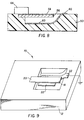
- Green beam 56 and green ribbon 58 should be fixtured such that movement of green beam 56 and green ribbon 58 relative to green base element 50 does not occur during the sintering process. Fixturing can be accomplished by using a weight 66 over that end of green beam 56 and green ribbon 58 residing in recess 44 (see Figure 8). Weight 66 can be made from a piece of sintered oxide ceramic such as alumina, magnesia, or zirconia. The green base element 50, green beam 56, green ribbon 58, and green laminate conductor 60 are then sintered in air at 1500°C for two hours to form the basic micromolded sintered reflector body 70 of the device 10 of the present invention, an example of which is depicted in Figure 9.
- the basic micromolded sintered reflector body 70 includes base element 12, beam 18, reflective and conductive ribbon 20, and electrically conductive laminate 22 which as a result of sintering are integrally connected.
- the preferred sintering schedule for sintering the green base element 50 and the green beam 56 is to sinter such green parts by sequentially:
- the powder employed in the present invention for forming base element 12 in its precompacted, presintered form comprises zirconium oxide alloyed with one or more secondary oxide powders as above stated.
- the powder should have certain properties in order to produce a ceramic of the invention consisting essentially of tetragonal phase, cubic and monoclinic phase-free, crystal grain structure.
- Particle size and distribution of the powder should be uniform, having an agglomerate size in the range of from about 30 ⁇ m to about 60 ⁇ m with an average of about 50 ⁇ m.
- “Agglomerate” can be defined as an aggregate of individual particles of the ceramic powder, and each particle may comprise multiple grains.
- Grain can be defined as crystals, within the particle, having a spatial orientation that is unaligned with or distinct from adjacent grains.
- the grain size should be in the range of from about 0.1 ⁇ m to about 6 ⁇ m, with a preferred size of about 0.3 ⁇ m.
- the term "net shape" as used herein, for example as in net shape ceramic or net shape part, means that the ceramic is dimensionally true after sintering and therefore should not necessitate further machining prior to use in its intended working environment. In other words, the dimensions both of the green part and the ceramic are predictable in that the amount of shrinkage of the green part during sintering is predictable, producing a ceramic part that conforms to a predetermined shape and dimensions.
- the amount of shrinkage along any axis of the compacted powder form to that of the net shape ceramic should be less than about 0.001 percent in order to obtain close, predictable dimensional tolerances and produce the net shape ceramic of the invention. Such a part can then be put in its intended use without having to carry out a machining operation. Purity of the material should also be well controlled in the range of from about 99.9 percent to 99.99 percent by weight; that is, impurities should be present in the amount of no more than about 0.1 to about 0.01 percent by weight.
- the moisture content of the powder should be maintained between about 0.2 to about 1.0 percent by volume of the powder when compacted. Too dry a powder can result in too porous a ceramic, and too high a moisture level can inhibit good release of the green parts from the mold surface. A preferred moisture content is about 0.5 percent.
- the powder is compacted into a green part by means of a die press or the like.
- the term "green part” as used herein means the powder in its compacted, presintered state.
- the powder should be compacted by applying uniform compacting forces to the powder in order to produce a green part having a uniform density.
- a preferred compacting device that achieves uniform compacting forces is a floating mold die press.
- the green part should have a predetermined density selected by the operator to produce, after sintering, a net shape ceramic article. For example, for specific compositions of powder described herein, a preferred green part density is in the range of from about 3.2 g/cc to about 3.5 g/cc.
- the compaction pressure determines the density of the green part and consequently that of the ceramic.
- the ceramic can have a lower than desired density and not attain the desired net shape. If the compaction pressure is too high, the green part can delaminate and result in a ceramic that is defective for the intended use, for example, for cutting.
- the compaction pressure for the above mentioned alloyed zirconia powders should be in the range of from about 10,000 psi to about 15,000 psi, and a preferred compaction pressure is about 12,000 psi.
- the compaction time can be readily determined by the operator depending on the compaction pressure selected.
- Compaction time for example, can be in the range of from about 60 seconds to 10 seconds for compaction pressures in the range of from about 10,000 psi to about 15,000 psi, respectively, and about 30 seconds for a compaction pressure of about 12,000 psi.
- the compacting is carried out for a time sufficient to compact the powder to form a green part having a predetermined density for the selected powder, for example, from about 3.0 g/cc to about 3.5 g/cc as above described. It is well known that the compaction pressure and time selected by the operator can be dependent on the size of the finished part. Generally, as the part size increases, compaction pressure and/or compaction time increase.
- the powder is compacted in the presence of an organic water-soluble binder, such as polyvinyl alcohol, gelatin, or a polyester ionomer.
- binder such as polyvinyl alcohol, gelatin, or a polyester ionomer.
- the binder can be added to and mixed with the powder, for example, by spray drying or ball milling, prior to placing the powder in the compacting device.
- an array 100 of micromolded integrated ceramic light reflectors 10 can be used in an image projection system.
- An image source 102 is received by a digital electrode controller 104.
- Digital electrode controller 104 individually controls the voltage supplies to each of the light reflectors 10 of array 100.
- a light source 106 transmits light in the visible range through the appropriate optics 108 to be incident upon array 100.
- a color filter 114 can be used to generate a color image.
Landscapes
- Physics & Mathematics (AREA)
- General Physics & Mathematics (AREA)
- Optics & Photonics (AREA)
- Optical Elements Other Than Lenses (AREA)
Applications Claiming Priority (2)
| Application Number | Priority Date | Filing Date | Title |
|---|---|---|---|
| US749715 | 1996-11-15 | ||
| US08/749,715 US5793519A (en) | 1996-11-15 | 1996-11-15 | Micromolded integrated ceramic light reflector |
Publications (1)
| Publication Number | Publication Date |
|---|---|
| EP0843191A1 true EP0843191A1 (de) | 1998-05-20 |
Family
ID=25014873
Family Applications (1)
| Application Number | Title | Priority Date | Filing Date |
|---|---|---|---|
| EP97203384A Withdrawn EP0843191A1 (de) | 1996-11-15 | 1997-10-31 | Mikrogeformter integrierter Keramiklichtreflektor |
Country Status (3)
| Country | Link |
|---|---|
| US (1) | US5793519A (de) |
| EP (1) | EP0843191A1 (de) |
| JP (1) | JPH10162613A (de) |
Cited By (2)
| Publication number | Priority date | Publication date | Assignee | Title |
|---|---|---|---|---|
| WO2004063089A3 (en) * | 2003-01-13 | 2004-11-04 | Indian Inst Of Technology Delh | Recessed microstructure device and fabrication method thereof |
| WO2019226627A1 (en) * | 2018-05-22 | 2019-11-28 | Corning Incorporated | Glazed ceramic substrate for liquid lenses and methods for making same |
Families Citing this family (65)
| Publication number | Priority date | Publication date | Assignee | Title |
|---|---|---|---|---|
| US5898515A (en) * | 1996-11-21 | 1999-04-27 | Eastman Kodak Company | Light reflecting micromachined cantilever |
| US5870221A (en) * | 1997-07-25 | 1999-02-09 | Lucent Technologies, Inc. | Micromechanical modulator having enhanced performance |
| US5910856A (en) * | 1998-04-16 | 1999-06-08 | Eastman Kodak Company | Integrated hybrid silicon-based micro-reflector |
| US6872984B1 (en) | 1998-07-29 | 2005-03-29 | Silicon Light Machines Corporation | Method of sealing a hermetic lid to a semiconductor die at an angle |
| US6303986B1 (en) | 1998-07-29 | 2001-10-16 | Silicon Light Machines | Method of and apparatus for sealing an hermetic lid to a semiconductor die |
| US5991079A (en) * | 1998-10-14 | 1999-11-23 | Eastman Kodak Company | Method of making a light modulator |
| US6014257A (en) * | 1998-10-14 | 2000-01-11 | Eastman Kodak Company | Light modulator |
| US6088148A (en) * | 1998-10-30 | 2000-07-11 | Eastman Kodak Company | Micromagnetic light modulator |
| US6392289B1 (en) | 1999-04-15 | 2002-05-21 | Micron Technology, Inc. | Integrated circuit substrate having through hole markings to indicate defective/non-defective status of same |
| US6236491B1 (en) * | 1999-05-27 | 2001-05-22 | Mcnc | Micromachined electrostatic actuator with air gap |
| US6741383B2 (en) | 2000-08-11 | 2004-05-25 | Reflectivity, Inc. | Deflectable micromirrors with stopping mechanisms |
| US6396619B1 (en) * | 2000-01-28 | 2002-05-28 | Reflectivity, Inc. | Deflectable spatial light modulator having stopping mechanisms |
| US6535318B1 (en) * | 1999-11-12 | 2003-03-18 | Jds Uniphase Corporation | Integrated optoelectronic devices having pop-up mirrors therein and methods of forming and operating same |
| US6956878B1 (en) | 2000-02-07 | 2005-10-18 | Silicon Light Machines Corporation | Method and apparatus for reducing laser speckle using polarization averaging |
| US7090189B2 (en) | 2001-01-17 | 2006-08-15 | Sandia National Laboratories | Compliant cantilevered micromold |
| US6947195B2 (en) * | 2001-01-18 | 2005-09-20 | Ricoh Company, Ltd. | Optical modulator, optical modulator manufacturing method, light information processing apparatus including optical modulator, image formation apparatus including optical modulator, and image projection and display apparatus including optical modulator |
| US7177081B2 (en) | 2001-03-08 | 2007-02-13 | Silicon Light Machines Corporation | High contrast grating light valve type device |
| JP3557525B2 (ja) * | 2001-03-29 | 2004-08-25 | 日本航空電子工業株式会社 | 微小可動デバイス |
| US6707591B2 (en) | 2001-04-10 | 2004-03-16 | Silicon Light Machines | Angled illumination for a single order light modulator based projection system |
| US6865346B1 (en) | 2001-06-05 | 2005-03-08 | Silicon Light Machines Corporation | Fiber optic transceiver |
| US6747781B2 (en) | 2001-06-25 | 2004-06-08 | Silicon Light Machines, Inc. | Method, apparatus, and diffuser for reducing laser speckle |
| US6782205B2 (en) | 2001-06-25 | 2004-08-24 | Silicon Light Machines | Method and apparatus for dynamic equalization in wavelength division multiplexing |
| US6829092B2 (en) | 2001-08-15 | 2004-12-07 | Silicon Light Machines, Inc. | Blazed grating light valve |
| US6930364B2 (en) | 2001-09-13 | 2005-08-16 | Silicon Light Machines Corporation | Microelectronic mechanical system and methods |
| US6956995B1 (en) | 2001-11-09 | 2005-10-18 | Silicon Light Machines Corporation | Optical communication arrangement |
| US6800238B1 (en) | 2002-01-15 | 2004-10-05 | Silicon Light Machines, Inc. | Method for domain patterning in low coercive field ferroelectrics |
| JP2003283242A (ja) * | 2002-03-25 | 2003-10-03 | Murata Mfg Co Ltd | 電波反射体及び該電波反射体が取り付けられた構造物 |
| US6767751B2 (en) | 2002-05-28 | 2004-07-27 | Silicon Light Machines, Inc. | Integrated driver process flow |
| US6728023B1 (en) | 2002-05-28 | 2004-04-27 | Silicon Light Machines | Optical device arrays with optimized image resolution |
| US7054515B1 (en) | 2002-05-30 | 2006-05-30 | Silicon Light Machines Corporation | Diffractive light modulator-based dynamic equalizer with integrated spectral monitor |
| US6822797B1 (en) | 2002-05-31 | 2004-11-23 | Silicon Light Machines, Inc. | Light modulator structure for producing high-contrast operation using zero-order light |
| US20040069742A1 (en) * | 2002-06-19 | 2004-04-15 | Pan Shaoher X. | Fabrication of a reflective spatial light modulator |
| US20030234994A1 (en) * | 2002-06-19 | 2003-12-25 | Pan Shaoher X. | Reflective spatial light modulator |
| US6992810B2 (en) * | 2002-06-19 | 2006-01-31 | Miradia Inc. | High fill ratio reflective spatial light modulator with hidden hinge |
| US7034984B2 (en) * | 2002-06-19 | 2006-04-25 | Miradia Inc. | Fabrication of a high fill ratio reflective spatial light modulator with hidden hinge |
| US6829258B1 (en) | 2002-06-26 | 2004-12-07 | Silicon Light Machines, Inc. | Rapidly tunable external cavity laser |
| US6714337B1 (en) | 2002-06-28 | 2004-03-30 | Silicon Light Machines | Method and device for modulating a light beam and having an improved gamma response |
| US6908201B2 (en) | 2002-06-28 | 2005-06-21 | Silicon Light Machines Corporation | Micro-support structures |
| US6813059B2 (en) | 2002-06-28 | 2004-11-02 | Silicon Light Machines, Inc. | Reduced formation of asperities in contact micro-structures |
| US6899838B2 (en) * | 2002-07-12 | 2005-05-31 | Becton, Dickinson And Company | Method of forming a mold and molding a micro-device |
| US6801354B1 (en) | 2002-08-20 | 2004-10-05 | Silicon Light Machines, Inc. | 2-D diffraction grating for substantially eliminating polarization dependent losses |
| US7057795B2 (en) | 2002-08-20 | 2006-06-06 | Silicon Light Machines Corporation | Micro-structures with individually addressable ribbon pairs |
| US6712480B1 (en) | 2002-09-27 | 2004-03-30 | Silicon Light Machines | Controlled curvature of stressed micro-structures |
| US6928207B1 (en) | 2002-12-12 | 2005-08-09 | Silicon Light Machines Corporation | Apparatus for selectively blocking WDM channels |
| US7057819B1 (en) | 2002-12-17 | 2006-06-06 | Silicon Light Machines Corporation | High contrast tilting ribbon blazed grating |
| US6987600B1 (en) | 2002-12-17 | 2006-01-17 | Silicon Light Machines Corporation | Arbitrary phase profile for better equalization in dynamic gain equalizer |
| US6934070B1 (en) | 2002-12-18 | 2005-08-23 | Silicon Light Machines Corporation | Chirped optical MEM device |
| US6927891B1 (en) | 2002-12-23 | 2005-08-09 | Silicon Light Machines Corporation | Tilt-able grating plane for improved crosstalk in 1×N blaze switches |
| US7068372B1 (en) | 2003-01-28 | 2006-06-27 | Silicon Light Machines Corporation | MEMS interferometer-based reconfigurable optical add-and-drop multiplexor |
| US7286764B1 (en) | 2003-02-03 | 2007-10-23 | Silicon Light Machines Corporation | Reconfigurable modulator-based optical add-and-drop multiplexer |
| US6947613B1 (en) | 2003-02-11 | 2005-09-20 | Silicon Light Machines Corporation | Wavelength selective switch and equalizer |
| US6922272B1 (en) | 2003-02-14 | 2005-07-26 | Silicon Light Machines Corporation | Method and apparatus for leveling thermal stress variations in multi-layer MEMS devices |
| US6806997B1 (en) | 2003-02-28 | 2004-10-19 | Silicon Light Machines, Inc. | Patterned diffractive light modulator ribbon for PDL reduction |
| US7391973B1 (en) | 2003-02-28 | 2008-06-24 | Silicon Light Machines Corporation | Two-stage gain equalizer |
| US6829077B1 (en) | 2003-02-28 | 2004-12-07 | Silicon Light Machines, Inc. | Diffractive light modulator with dynamically rotatable diffraction plane |
| US7027202B1 (en) | 2003-02-28 | 2006-04-11 | Silicon Light Machines Corp | Silicon substrate as a light modulator sacrificial layer |
| US6922273B1 (en) | 2003-02-28 | 2005-07-26 | Silicon Light Machines Corporation | PDL mitigation structure for diffractive MEMS and gratings |
| US7042611B1 (en) | 2003-03-03 | 2006-05-09 | Silicon Light Machines Corporation | Pre-deflected bias ribbons |
| US7026695B2 (en) * | 2003-11-19 | 2006-04-11 | Miradia Inc. | Method and apparatus to reduce parasitic forces in electro-mechanical systems |
| US7042619B1 (en) * | 2004-06-18 | 2006-05-09 | Miradia Inc. | Mirror structure with single crystal silicon cross-member |
| US7068417B2 (en) * | 2004-07-28 | 2006-06-27 | Miradia Inc. | Method and apparatus for a reflective spatial light modulator with a flexible pedestal |
| US7202989B2 (en) | 2005-06-01 | 2007-04-10 | Miradia Inc. | Method and device for fabricating a release structure to facilitate bonding of mirror devices onto a substrate |
| US7190508B2 (en) * | 2005-06-15 | 2007-03-13 | Miradia Inc. | Method and structure of patterning landing pad structures for spatial light modulators |
| US7184195B2 (en) | 2005-06-15 | 2007-02-27 | Miradia Inc. | Method and structure reducing parasitic influences of deflection devices in an integrated spatial light modulator |
| US7382513B2 (en) * | 2005-10-13 | 2008-06-03 | Miradia Inc. | Spatial light modulator with multi-layer landing structures |
Citations (3)
| Publication number | Priority date | Publication date | Assignee | Title |
|---|---|---|---|---|
| WO1992004170A2 (en) * | 1990-09-04 | 1992-03-19 | Holl Richard A | Method of manufacturing articles from powdered materials |
| US5506720A (en) * | 1993-09-28 | 1996-04-09 | Daewoo Electronics Co., Ltd. | Method for manufacturing an electrodisplacive actuated mirror array |
| WO1996033437A1 (en) * | 1995-04-17 | 1996-10-24 | Aura Systems, Inc. | Monomorph thin film actuated mirror array |
Family Cites Families (11)
| Publication number | Priority date | Publication date | Assignee | Title |
|---|---|---|---|---|
| US3544201A (en) * | 1968-01-02 | 1970-12-01 | Gen Telephone & Elect | Optical beam deflector |
| US4492435A (en) * | 1982-07-02 | 1985-01-08 | Xerox Corporation | Multiple array full width electro mechanical modulator |
| US4450458A (en) * | 1982-07-02 | 1984-05-22 | Xerox Corporation | Multi-function reproduction apparatus |
| US4717893A (en) * | 1984-05-04 | 1988-01-05 | Hamamatsu Photonics Kabushiki Kaisha | Spatial light modulator |
| US5172262A (en) * | 1985-10-30 | 1992-12-15 | Texas Instruments Incorporated | Spatial light modulator and method |
| EP0246547A3 (de) * | 1986-05-22 | 1990-06-13 | Siemens Aktiengesellschaft | Anordnung zur optischen Bildverarbeitung |
| US4793697A (en) * | 1986-08-04 | 1988-12-27 | Motorola, Inc. | PLZT shutter with minimized space charge degradation |
| US4805038A (en) * | 1987-07-30 | 1989-02-14 | Eastman Kodak Company | Imaging apparatus which includes a light-valve array having electrostatically deflectable elements |
| US5266531A (en) * | 1991-01-30 | 1993-11-30 | Cordata Incorporated | Dynamic holographic display with cantilever |
| US5336282A (en) * | 1991-12-31 | 1994-08-09 | Eastman Kodak Company | Zirconia ceramics and a process of producing the same |
| US5579151A (en) * | 1995-02-17 | 1996-11-26 | Texas Instruments Incorporated | Spatial light modulator |
-
1996
- 1996-11-15 US US08/749,715 patent/US5793519A/en not_active Expired - Fee Related
-
1997
- 1997-10-31 EP EP97203384A patent/EP0843191A1/de not_active Withdrawn
- 1997-11-14 JP JP9313235A patent/JPH10162613A/ja active Pending
Patent Citations (3)
| Publication number | Priority date | Publication date | Assignee | Title |
|---|---|---|---|---|
| WO1992004170A2 (en) * | 1990-09-04 | 1992-03-19 | Holl Richard A | Method of manufacturing articles from powdered materials |
| US5506720A (en) * | 1993-09-28 | 1996-04-09 | Daewoo Electronics Co., Ltd. | Method for manufacturing an electrodisplacive actuated mirror array |
| WO1996033437A1 (en) * | 1995-04-17 | 1996-10-24 | Aura Systems, Inc. | Monomorph thin film actuated mirror array |
Non-Patent Citations (2)
| Title |
|---|
| PETER BARYSCH: "MIKROSPIEGEL IN DER GROSSBILDPROJEKTION", FUNKSCHAU, vol. 67, no. 19, 1 September 1995 (1995-09-01), pages 34/35, XP000530294 * |
| PETERSEN K E: "MICROCHANICAL LIGHT DEFLECTOR ARRAY", IBM TECHNICAL DISCLOSURE BULLETIN, vol. 20, no. 1, 1 June 1977 (1977-06-01), pages 355/356, XP002001788 * |
Cited By (2)
| Publication number | Priority date | Publication date | Assignee | Title |
|---|---|---|---|---|
| WO2004063089A3 (en) * | 2003-01-13 | 2004-11-04 | Indian Inst Of Technology Delh | Recessed microstructure device and fabrication method thereof |
| WO2019226627A1 (en) * | 2018-05-22 | 2019-11-28 | Corning Incorporated | Glazed ceramic substrate for liquid lenses and methods for making same |
Also Published As
| Publication number | Publication date |
|---|---|
| US5793519A (en) | 1998-08-11 |
| JPH10162613A (ja) | 1998-06-19 |
Similar Documents
| Publication | Publication Date | Title |
|---|---|---|
| US5793519A (en) | Micromolded integrated ceramic light reflector | |
| US5735985A (en) | Method for micromolding ceramic structures | |
| US6265811B1 (en) | Ceramic element, method for producing ceramic element, display device, relay device and capacitor | |
| US5910856A (en) | Integrated hybrid silicon-based micro-reflector | |
| JPWO1998024130A1 (ja) | セラミック素子、セラミック素子の製造方法、表示装置、リレー装置及びコンデンサ | |
| EP0766325B1 (de) | Piezoeletrisches/elektrostriktives Dünnfilmelement und Herstellungsverfahren | |
| US5504388A (en) | Piezoelectric/electrostrictive element having electrode film(s) with specified surface roughness | |
| EP0606767B1 (de) | Piezoelektrische Anordnung | |
| EP0671772B1 (de) | Verfahren zur Herstellung einer Membranstruktur aus Keramik mit einem konvexen Teil | |
| Hassanin et al. | Micro-fabrication of ceramics: Additive manufacturing and conventional technologies | |
| EP0701112B1 (de) | Membranstruktur aus Keramik mit einem konvexen Teil und Verfahren zu ihrer Herstellung | |
| US20040017133A1 (en) | Piezoelectric/electrostrictive device and method of manufacturing same | |
| US20080225370A1 (en) | Low-cost continuous phase sheet deformable mirror | |
| US6323582B1 (en) | Piezoelectric/Electrostrictive device | |
| US6931698B2 (en) | Method for fabricating piezoelectric/electrostrictive device | |
| EP1642875A2 (de) | Piezoelektrische/elektrostriktive keramische Zusammensetzung | |
| US6476539B1 (en) | Piezoelectric/electrostrictive device | |
| US7332851B2 (en) | Piezoelectric/electrostrictive film type device and method of manufacturing the same | |
| EP1089351A2 (de) | Piezoelektrisches/elektrostriktives Bauelement | |
| JPH11339561A (ja) | セラミック素子、セラミック素子の製造方法、表示装置、リレー装置及びコンデンサ | |
| WO2006035723A1 (ja) | 圧電/電歪膜型素子及びその製造方法 | |
| US20060113876A1 (en) | Piezoelectric/electrostrictive device | |
| US7007355B2 (en) | Method of manufacturing a piezoelectric/electrostrictive device | |
| Wang et al. | Processing of PZT microstructures | |
| US5795422A (en) | Method for forming molded ceramic devices having embedded spiral coils |
Legal Events
| Date | Code | Title | Description |
|---|---|---|---|
| PUAI | Public reference made under article 153(3) epc to a published international application that has entered the european phase |
Free format text: ORIGINAL CODE: 0009012 |
|
| STAA | Information on the status of an ep patent application or granted ep patent |
Free format text: STATUS: THE APPLICATION HAS BEEN WITHDRAWN |
|
| AK | Designated contracting states |
Kind code of ref document: A1 Designated state(s): AT BE CH DE DK ES FI FR GB GR IE IT LI LU MC NL PT SE |
|
| AX | Request for extension of the european patent |
Free format text: AL;LT;LV;RO;SI |
|
| 18W | Application withdrawn |
Withdrawal date: 19980411 |