EP0843232A2 - Appareil pour générer des données d'impulsions en durées pour un appareil d'impression du type de transfert de toner - Google Patents
Appareil pour générer des données d'impulsions en durées pour un appareil d'impression du type de transfert de toner Download PDFInfo
- Publication number
- EP0843232A2 EP0843232A2 EP97309307A EP97309307A EP0843232A2 EP 0843232 A2 EP0843232 A2 EP 0843232A2 EP 97309307 A EP97309307 A EP 97309307A EP 97309307 A EP97309307 A EP 97309307A EP 0843232 A2 EP0843232 A2 EP 0843232A2
- Authority
- EP
- European Patent Office
- Prior art keywords
- pulse
- pixel
- data
- width
- width data
- Prior art date
- Legal status (The legal status is an assumption and is not a legal conclusion. Google has not performed a legal analysis and makes no representation as to the accuracy of the status listed.)
- Granted
Links
- 239000011159 matrix material Substances 0.000 abstract description 14
- 230000016776 visual perception Effects 0.000 description 10
- 238000010586 diagram Methods 0.000 description 8
- 238000000034 method Methods 0.000 description 5
- 239000002245 particle Substances 0.000 description 4
- 241001270131 Agaricus moelleri Species 0.000 description 1
- 238000010276 construction Methods 0.000 description 1
- 238000007796 conventional method Methods 0.000 description 1
- 230000007613 environmental effect Effects 0.000 description 1
Images


Classifications
-
- H—ELECTRICITY
- H04—ELECTRIC COMMUNICATION TECHNIQUE
- H04N—PICTORIAL COMMUNICATION, e.g. TELEVISION
- H04N1/00—Scanning, transmission or reproduction of documents or the like, e.g. facsimile transmission; Details thereof
- H04N1/40—Picture signal circuits
- H04N1/405—Halftoning, i.e. converting the picture signal of a continuous-tone original into a corresponding signal showing only two levels
- H04N1/4055—Halftoning, i.e. converting the picture signal of a continuous-tone original into a corresponding signal showing only two levels producing a clustered dots or a size modulated halftone pattern
- H04N1/4056—Halftoning, i.e. converting the picture signal of a continuous-tone original into a corresponding signal showing only two levels producing a clustered dots or a size modulated halftone pattern the pattern varying in one dimension only, e.g. dash length, pulse width modulation [PWM]
Definitions
- the present invention relates to an apparatus for generating pulse-width data for expressing a multiplicity of gray scales to supply the pulse-width data to a printing engine of a toner-transfer-type printing apparatus, such as a laser printer or a copying machine.
- a toner-transfer-type printing apparatus is able to print a multi-gray-scale image by adjusting the pulse width of a drive pulse signal for driving drawing laser in a printing engine because the quantity of toner for each pixel to be allowed to adhere can be changed. Since the minimum size of toner particles however is limited, the number of gray scale levels, which can be expressed, is reduced in inverse proportion to the resolution of an image required to be printed.
- An assumption is made that image data having a resolution of 600 dpi and 256 gray scale levels is created on a personal computer and image data above is printed by a laser printer having a printing resolution of 600 dpi.
- One pixel having a resolution of 600 dpi is in the form of a square region, one side of which is 1/600 inch.
- the number of toner particles allowed to adhere to the square region is limited to about 20 to 30. Therefore, the image printed by the laser printer is able to reproduce at most 20 to 30 gray scale levels.
- the conventional toner-transfer-type printing apparatus suffers from a problem in that the apparatus cannot reproduce a number of gray scale levels on a print output therefrom even if image data expressing the number of gray scale levels exceeding the number of toner particles allowed to adhere to one pixel region is supplied.
- an object of the present invention is to enable a toner-transfer-type printing apparatus to reproduce, on an output image therefrom, a number of gray scale levels which is larger than the number of toner particles allowed to adhere to one pixel region, and more specifically to print an output image with which the sense of sight of a human being recognizes a fact that such a large number of gray scale levels has been reproduced.
- a pulse-width data generating apparatus for use in a toner-transfer-type printing apparatus.
- the apparatus according to the present invention generates pulse-width data for each pixel of an output image in accordance with gray-scale data of each pixel in image data.
- the apparatus according to the present invention has a memory for converting gray-scale data of each pixel of image data into pulse-width data of each pixel of an output image.
- the memory has N ⁇ M pixel memory regions corresponding to N ⁇ M pixels disposed to form N ⁇ M pixel matrices on the output image (N and M are positive integers).
- pulse-width data items corresponding to various values which are possible for gray-scale data to have, are stored in each of the pixel memory regions.
- pulse-width data corresponding to gray-scale data is read from the pixel memory region in the memory instructed with the coordinates.
- the pulse-width data generating apparatus enables the overall N ⁇ M matrices on the output image to reproduce the number of gray scale levels which is about N ⁇ M times the number of gray scale levels which can be expressed by one pixel.
- N ⁇ M the number of gray scale levels which can be expressed by one pixel.
- a required gray scale with an appropriate size near the minimum limit for the sense of sight for a human being, such as 2 ⁇ 2 pixel matrices (corresponding to 300 dpi) or 3 ⁇ 3 pixel matrices (corresponding to 200 dpi), enables for the sense of sight for a human being to recognize as if the required number of the gray scale levels has been reproduced on the output image.
- an inverted ⁇ -characteristic for correcting a ⁇ -characteristic of the printing engine is incorporated to pulse-width data in the memory.
- a structure in which the inverted ⁇ -characteristics incorporated to pulse-width data are made to be slightly different from one another among the pixel memory regions causes a precise inverted ⁇ -characteristic to appear in pulse-width data of the overall N ⁇ M matrices attributable to a principle like the above-mentioned principle with which the number of gray scale levels which can be expressed increases. As a result, precise ⁇ -correction can be performed.
- the apparatus according to the present invention further comprises position-data generating means which receives pulse-width data read from the memory to subject pulse-width data items of pixels on the two sides of each pixel on the output image to a comparison to generate position data corresponding to a result of the comparison, position data being generated for each pixel on the output image.
- Position data generated by the above-mentioned means indicates a pixel of the pixels on the two sides of each pixel on the output image that has higher density.
- the process for collecting the positions, at each of which toner is allowed to adhere to form pixels, to integrate dots has a conventional technique for improving the quality of an output image.
- the apparatus according to the present invention arranged in such a manner that the toner adhesion position is automatically determined in accordance with pulse-width data for each pixel read from the memory, enables a necessity of previously providing, to image data, position data for instructing the toner adhesion position to be eliminated.
- an advantage can be realized in that the capacity of the image memory for storing image data can be saved by the foregoing degree.
- Fig. 1 shows an overall structure of an embodiment of a laser printer including a pulse generating circuit according to the present invention.
- a laser printer 200 has a main processor (a microcomputer) 300.
- the main processor 300 processes sequential printing commands supplied from a host computer 100 to generate a bit-map type image data 400.
- Image data 400 is stored in an image memory 500.
- a pulse generating circuit 600 according to the present invention is connected to the image memory 500.
- the pulse generating circuit 600 makes a direct memory access (DMA) to read image data 400 from the image memory 500 so as to generate, from gray-scale data of each pixel of image data 400, a laser drive pulse for driving a drawing laser in a printing engine 700.
- DMA direct memory access
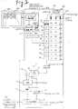
- Fig. 2 shows the structure of the pulse generating circuit 600.
- Figs. 3 (A) to 3 (C) shows the operation of the pulse generating circuit 600.
- the pulse generating circuit 600 includes an address generating circuit 1, a RAM 3, a shift register 4, a comparator 5 and a pulse modulation circuit 6.
- the address generating circuit 1 generates address data for pixels P00, P01, P20,..., of image data 400 in the image memory 500 to supply address data to the image memory 500.
- the image memory 500 responds each of the pixel address data items to output gray-scale data 23 of each of the pixels P00, P01, P20,..., of image data 400 to the pulse generating circuit 600.
- Gray-scale data of each of the pixels P00, P01, P20,..., of image data 400 is, for example, 8-bit data. Namely, the gray scale value of each pixel is expressed by 256 levels.
- the RAM 3 has nine pixel memory regions 31 to 39.
- Each of the pixel memory regions 31 to 39 corresponds to nine pixels a to i which form, on an output image which must be printed out, one 3 ⁇ 3 pixel matrix 7 as shown in Fig. 3 (B).
- 256 eight-bit words (indicated with xxxxxxxx) are stored.
- Each eight-bit word indicates the pulse width of a laser drive pulse which is supplied to the printing engine 700.
- the pulse width By adjusting the pulse width, the quantity of toner for each pixel on the output image, that is, the gray scale can be adjusted. Therefore, 256 types of 8-bit pulse-width data items for changing the gradations of the corresponding pixels a to i on the output image are stored in each of the pixel memory regions 31 to 39.
- All of the pulse-width data items are previously programmed in a ROM (not shown) in the laser printer so as to be loaded from the ROM to the RAM 3 when, for example, the laser printer is turned on. It is preferable that standard pulse-width data read from the ROM be subjected to correction which is performed in consideration of the environmental conditions, including the temperature, humidity and power supply voltage at the loading operation and then corrected pulse-width data be stored in the RAM 3.
- Each pulse-width data in the RAM 3 is addressed with a 12-bit address word 2.
- the address word 2 includes a 2-bit vertical coordinate data 21, 2-bit horizontal coordinate data 22 and 8-bit (having 256 gray scale levels) gray-scale data 23.
- Vertical coordinate data 21 and horizontal coordinate data 22 are generated by the address generating circuit 1 in accordance with each of the pixel address data items to indicate the vertical coordinates and the horizontal coordinates of each pixel of one 3 ⁇ 3 pixel matrix 7 on the output image shown in Fig. 3 (B).
- Eight-bit gray-scale data 23 is each pixel data of image data 400 read from the image memory 500.
- Each pixel of image data 400 in the image memory 500 is sequentially addressed in the order of raster scan by the address generating circuit 1. Therefore, as shown in Fig. 3 (A), reading starts at pixel P00 at the left-hand end of the uppermost line, and then pixels P10, P20, P30,..., on the uppermost line are sequentially read. Then, pixels P01, P11, P21, P31,...., on the second line are, similarly, sequentially read, and then pixels on the third line are read. The foregoing operation is repeated to reach the lowermost line.
- Each pixel in the 3 ⁇ 3 pixel matrix 7 on the output image as shown in Fig. 3 (B) is made to correspond to each pixel of image data 400.
- each of all of the pixels of image data 400 are made to correspond to any one of the pixel in the 3 ⁇ 3 pixel matrix 7.
- pixels P00, P10, P20, P30 and P40 of image data 400 correspond to pixels a, b, c, a and b of the 3 ⁇ 3 pixel matrix 7, respectively.
- the address generating circuit 1 generates, from the address data of each pixel, the above-mentioned vertical coordinate data 21 and horizontal coordinate data 22 for each pixel.
- the shift register 4 has three stages 41, 42 and 43 and receives pulse-width data sequentially read from the RAM 3 by the first stage 41 thereof to sequentially transfer the same to the second stage 42 and the third stage 43.
- the shift register 4 is caused to always have pulse-width data of three pixels Pn-1, Pn and Pn+1 continued in the horizontal direction on image data 400.
- the three pixels Pn-1, Pn and Pn+1 move on the image along the raster scanning passage.
- pulse-width data of pixels P00, P10 and P20 is stored in the shift register 4 at time tl as shown in Fig.
- pulse-width data of pixels P10, P20 and P30 shifted to the right by one pixel is stored in next time t2, and then pulse-width data P20, P30 and P40 further shifted by one pixel is stored at next time t3.
- Pulse-width data items of pixels Pn-1 and Pn+1 in the stages 43 and 41 at the two ends of the shift register 4 are supplied to the comparator 5.
- the comparator 5 subjects pulse-width data items of the two pixels Pn-1 and Pn+1 to a comparison to output 2-bit position data 61 indicating the position of a pixel having a larger pulse width (that is, a pixel having a higher density). If the right-hand pixel Pn+1 has a higher density, "00" is output as position data 61. If the left-hand pixel Pn-1 has a higher density, "10” is output. If the densities of the two pixels Pn-1 and Pn+1 are the same, "11” is output. Position data 61 above is supplied to the pulse modulation circuit 6. Pulse-width data 62 of pixel Pn in the central stage 42 of the shift register 4 is directly supplied to the pulse modulation circuit 6.
- the pulse modulation circuit 6 In accordance with 2-bit position data 61 and 8-bit pulse-width data 62, the pulse modulation circuit 6 generates a laser drive pulse for drawing the central pixel Pn as follows: the pulse width (a duty ratio) of the laser drive pulse is determined in accordance with 8-bit pulse-width data 62. Therefore, the duty ratio of the drive pulse, that is, the gray scale value of the pixel is modulated to 256 levels.
- the position of the laser drive pulse in terms of time that is, the spatial position in the pixel region to which toner is allowed to adhere is determined to be in the right-half portion if position data 61 is "00". If data above is "10", the position is determined to be in the left-half portion. If data above is "11", the position is determined to be the center. That is, the toner adhesion position is approached to the pixel Pn-1 or the pixel Pn+1 adjacent laterally that has a higher density.
- a drive pulse the pulse width of which has been modulated to 256 levels, is generated for each pixel so as to be supplied to the printing engine 700 so that a laser beam for drawing an electrostatic latent image is modulated.
- a printing engine having printing performance of a resolution of 600 dpi is able to express gradation of at most 20 to 30 levels for each pixel even if a drive pulse modulated to 256 levels is supplied. That is, only the number of gray scale levels which is the same as that when the pulse width of a laser drive pulse has been modulated to 20 to 30 levels can be reproduced.
- the above-mentioned pulse generating circuit 600 arranged to slightly change pulse-width data items in the RAM 3 for each pixel, is able to cause the sense of sight of a human being to recognize as if 256 gray scale levels has been expressed.
- Figs. 5 (A) to 5 (C) shows a principle of the foregoing structure.
- a model formed by simplifying the above-mentioned circuit 600 will now be described.
- a matrix having four pixels w, x, y and z is assumed.
- An assumption is further made that gray-scale data has 9 levels from 0 to 8 for each pixel.
- another assumption is made that the substantial number of gray scale levels (that is, the gray scale levels of one pixel which can be reproduced by the engine) of the pulse width of the laser drive pulse is three levels from 0 to 2.
- the pulse generating circuit 600 has a structure that pulse-width data items, which are slightly different from one another, are stored in the nine pixel memory regions 31 to 39 in the RAM 3.
- the pulse widths of the nine pixels a to i are averaged in the overall 3 ⁇ _ 3 pixel matrix shown in Fig. 3 (B) so that the number of gray scale levels which is nine times the 20 to 30 levels each of which is the substantial number of gray scale levels of each pixel is expressed.
- the sense of sight for a human being usually integrally recognizes pixels in the 3 ⁇ _ 3 pixel matrix in place of recognizing the same individually. Therefore, the sense of sight for a human being recognizes that 256 levels have been reproduced in the printed out image.
- the circuit according to this embodiment is arranged in such a manner that an inverted ⁇ -characteristic which is inversion to the ⁇ -characteristic of the printing engine is incorporated to pulse-width data in the RAM 3 in order to correct the ⁇ -characteristic of the printing engine.
- Fig. 6 (A) shows a ⁇ -characteristic 70 of the printing engine and an inverted ⁇ -characteristic 80 incorporated to pulse-width data.
- the pulse width of the drive pulse and the actual quantity of toner which is allowed to adhere have not a linear relationship.
- the change ratio of the toner adhesion quantity with respect to the pulse width is reduced in a region in which the pulse width (the duty ratio) is near the maximum value (a dense region). Therefore, the inverted ⁇ -characteristic 80 is incorporated to the relationship of the pulse width with respect to gray-scale data so that the relationship of the toner adhesion quantity with respect to gray-scale data is made to be linear and thus the ⁇ -characteristic is corrected, as shown in Fig. 6 (B).
- the pulse generating circuit 600 uses a principle like the principle described with reference to Figs. 5 (A) to 5 (C) in order to precisely perform the ⁇ -correction. That is, the inverted ⁇ -characteristic 80 incorporated to pulse-width data in the RAM 3 is made to be slightly different among the pixel memory regions so that a precise inverted ⁇ -characteristic is realized in the 3 ⁇ 3 pixel matrix 7 shown in Fig. 3 (B).
- Figs. 7 (A) and 7 (B) show the above-mentioned principle by using the simplified 4-pixel matrix model shown in Fig. 5 (A).
- an inverted ⁇ -characteristic in the form in which the four pixels are integrated as shown in Fig. 7 (B) appears.
- the inverted ⁇ -characteristic in the integrated form shown in Fig. 7 (B) is subjected to a comparison with the inverted ⁇ -characteristic of one pixel shown in Fig. 7 (A)
- the inverted ⁇ -characteristic in the integrated form has substantially 16 modulation levels of pulse width which is four times the number of modulation levels realized by the inverted ⁇ -characteristic of one pixel which is four levels. Therefore, precise ⁇ -correction can be performed.
- the pulse generating circuit 600 is effective when image data 400 having a resolution lower than that of the printing engine is processed.
- An assumption is made that the resolution of the printing engine is, for example, 600 dpi.
- the address generating circuit 1 generates one address word 2 for each pixel to supply the same to the RAM 3 when the address generating circuit 1 processes image data having a resolution of 600 dpi which is the same as that of the engine.
- the address generating circuit 1 When image data 400 having a resolution of, for example, 200 dpi which is lower than the resolution of the engine is processed, the address generating circuit 1 repeatedly scans each line of 200-dpi image data 400 three times because one 200 dpi pixel includes nine 600-dpi pixels a to i as shown in Fig. 8 to repeatedly read gray-scale data of each pixel on each line three time so as to generate vertical and horizontal address data items 21 and 22 of one pixel among the nine 600-dpi pixels a to i.
- nine laser drive pulses for drawing nine 600-dpi pixels can be generated from 200-dpi gray-scale data of one pixel.
- real 256 gray scale levels can be reproduced for each 200-dpi pixel. Note that the above-mentioned process which is performed by the address generating circuit 1 can be realized by software as well as an exclusive hardware.
- the pulse generating circuit 600 has the structure that gray-scale data is converted into pulse-width data by reading pulse-width data from the RAM 3 as shown in Fig. 2 in place of employing a software process. Therefore, an advantage is realized in that the capacity of the image memory for storing image data can be reduced when image data having a resolution lower than the performance of the engine is processed. If the operation, which is performed by the circuit according to this embodiment, is carried out by a software operation to process, for example, 200-dpi image data, software above must divide one 200-dpi pixel into nine 600-dpi pixels after which it generates pulse-width data (a gray scale value) for each of the nine 600-dpi pixels, as shown in Fig. 9.
Landscapes
- Engineering & Computer Science (AREA)
- Multimedia (AREA)
- Signal Processing (AREA)
- Facsimile Image Signal Circuits (AREA)
- Dot-Matrix Printers And Others (AREA)
- Laser Beam Printer (AREA)
- Control Or Security For Electrophotography (AREA)
- Record Information Processing For Printing (AREA)
Applications Claiming Priority (3)
| Application Number | Priority Date | Filing Date | Title |
|---|---|---|---|
| JP30841096 | 1996-11-19 | ||
| JP308410/96 | 1996-11-19 | ||
| JP30841096A JP3156605B2 (ja) | 1996-11-19 | 1996-11-19 | トナー転写式の印刷装置のためのパルス幅データの生成装置及び方法 |
Publications (3)
| Publication Number | Publication Date |
|---|---|
| EP0843232A2 true EP0843232A2 (fr) | 1998-05-20 |
| EP0843232A3 EP0843232A3 (fr) | 1998-12-23 |
| EP0843232B1 EP0843232B1 (fr) | 2003-10-15 |
Family
ID=17980733
Family Applications (1)
| Application Number | Title | Priority Date | Filing Date |
|---|---|---|---|
| EP97309307A Expired - Lifetime EP0843232B1 (fr) | 1996-11-19 | 1997-11-19 | Appareil pour générer des données d'impulsions en durées pour un appareil d'impression du type de transfert de toner |
Country Status (4)
| Country | Link |
|---|---|
| US (1) | US6369911B1 (fr) |
| EP (1) | EP0843232B1 (fr) |
| JP (1) | JP3156605B2 (fr) |
| DE (1) | DE69725536T2 (fr) |
Cited By (4)
| Publication number | Priority date | Publication date | Assignee | Title |
|---|---|---|---|---|
| EP1026878A3 (fr) * | 1999-02-05 | 2002-01-02 | Seiko Epson Corporation | Appareil électrophotographique en couleurs et procédé pour le traitement d'une image produite par celui-ci |
| EP1178671A1 (fr) * | 2000-08-03 | 2002-02-06 | Seiko Epson Corporation | Appareil électrophotographique de formation d'image et produit logiciel de formation d'image |
| EP1229730A1 (fr) * | 2001-02-02 | 2002-08-07 | Ricoh Company, Ltd. | Appareil et procédé de formation d'images |
| GB2405510A (en) * | 2003-08-27 | 2005-03-02 | Agilent Technologies Inc | Printing data |
Families Citing this family (20)
| Publication number | Priority date | Publication date | Assignee | Title |
|---|---|---|---|---|
| US6791713B1 (en) * | 1998-10-13 | 2004-09-14 | Ricoh Company, Ltd. | Image forming apparatus |
| JP3844180B2 (ja) * | 1999-09-27 | 2006-11-08 | リコープリンティングシステムズ株式会社 | 分割分散pwm階調処理装置及びこれを備えたレーザプリンタ |
| US7280246B2 (en) * | 2003-02-12 | 2007-10-09 | Marvell International Technology Ltd. | Laser print apparatus that generates pulse width value and justification value based on pixels in a multi-bit image |
| US8368950B2 (en) * | 2003-10-06 | 2013-02-05 | Marvell International Technology Ltd. | Method of pre-processing data on a host machine for a host-based print system |
| US7480066B2 (en) * | 2004-07-29 | 2009-01-20 | Marvell International Technology Ltd. | Modulated video waveform generator |
| JP2006074305A (ja) * | 2004-09-01 | 2006-03-16 | Ricoh Co Ltd | 階調再現方法、画像形成装置及びプリンタドライバ |
| US20070109568A1 (en) * | 2005-11-17 | 2007-05-17 | Keithley Douglas G | Method and apparatus for printing an image |
| US20070269123A1 (en) * | 2006-05-16 | 2007-11-22 | Randall Don Briggs | Method and apparatus for performing image enhancement in an image processing pipeline |
| US7957025B2 (en) * | 2006-06-30 | 2011-06-07 | Konica Minolta Systems Laboratory, Inc. | Systems and methods for processing pixel data for a printer |
| US7907303B2 (en) * | 2006-06-30 | 2011-03-15 | Konica Minolta Systems Laboratory, Inc. | Systems and methods for processing pixel data for a printer |
| US7822115B2 (en) * | 2006-06-30 | 2010-10-26 | Konica Minolta Systems Laboratory, Inc. | Systems for generating a pulse width modulated signal |
| US20080002229A1 (en) * | 2006-06-30 | 2008-01-03 | Konica Minolta Systems Laboratory, Inc. | Systems and method for saving memory on screen |
| JP4918871B2 (ja) * | 2007-02-27 | 2012-04-18 | セイコーエプソン株式会社 | プリンタ及びその制御方法 |
| WO2009070434A1 (fr) * | 2007-11-27 | 2009-06-04 | 3M Innovative Properties Company | Procédés de formation de feuille avec une image composite qui flotte et un outillage maître |
| US8782371B2 (en) * | 2008-03-31 | 2014-07-15 | Konica Minolta Laboratory U.S.A., Inc. | Systems and methods for memory management for rasterization |
| US8817032B2 (en) * | 2008-08-29 | 2014-08-26 | Konica Minolta Laboratory U.S.A., Inc. | Systems and methods for framebuffer management |
| US8854680B2 (en) * | 2008-09-11 | 2014-10-07 | Konica Minolta Laboratory U.S.A., Inc. | Systems and methods for optimal memory allocation units |
| US8861014B2 (en) * | 2008-09-30 | 2014-10-14 | Konica Minolta Laboratory U.S.A., Inc. | Systems and methods for optimized printer throughput in a multi-core environment |
| US8320012B2 (en) * | 2009-03-27 | 2012-11-27 | Konica Minolta Laboratory U.S.A., Inc. | Apparatus, system, and method for color data printing |
| US8223390B2 (en) * | 2009-03-27 | 2012-07-17 | Konica Minolta Laboratory U.S.A., Inc. | Systems and methods for reducing color registration errors in tandem engines |
Family Cites Families (16)
| Publication number | Priority date | Publication date | Assignee | Title |
|---|---|---|---|---|
| US4532503A (en) | 1982-11-08 | 1985-07-30 | International Business Machines Corporation | Sequence controlled pixel configuration |
| US4625330A (en) * | 1983-12-19 | 1986-11-25 | Ncr Corporation | Video enhancement system |
| DE3650599T2 (de) | 1985-08-15 | 1997-06-12 | Canon Kk | Vorrichtung zur Verarbeitung und Wiedergabe digitaler Videosignale, mit auf den Pixeltakt synchronisierter Pulsbreitenmodulation zur Erzeugung eines binären Signals aus Halbton-Bilddaten |
| DE3542484A1 (de) * | 1985-11-30 | 1987-07-02 | Ant Nachrichtentech | Verfahren zur erkennung von kantenstrukturen in einem bildsignal |
| JP3124016B2 (ja) | 1990-03-16 | 2001-01-15 | 株式会社東芝 | 画像形成装置 |
| US5287209A (en) | 1990-10-09 | 1994-02-15 | Matsushita Electric Industrial Co., Ltd. | Image forming device for enhancing tone reproduction by changing dot size |
| DE69220819T2 (de) * | 1991-02-01 | 1997-11-20 | Canon Kk | Bildverarbeitungsverfahren und -gerät |
| JPH04261264A (ja) * | 1991-02-15 | 1992-09-17 | Victor Co Of Japan Ltd | パルス幅変調装置 |
| US5495341A (en) | 1991-03-06 | 1996-02-27 | Canon Kabushiki Kaisha | Image processing apparatus which selects from one of plural generated clock counts |
| US5486927A (en) | 1991-08-19 | 1996-01-23 | Konica Corporation | Digital image forming apparatus using subdivided pixels |
| US5396584A (en) * | 1992-05-29 | 1995-03-07 | Destiny Technology Corporation | Multi-bit image edge enhancement method and apparatus |
| JPH06227033A (ja) * | 1993-02-01 | 1994-08-16 | Minolta Camera Co Ltd | デジタル画像形成装置 |
| WO1995002938A1 (fr) | 1993-07-12 | 1995-01-26 | Agfa-Gevaert Naamloze Vennootschap | Impression de haute qualite en demi-teinte a plusieurs niveaux destinee aux images couleur avec un encombrement memoire reduit |
| US5646670A (en) * | 1993-08-31 | 1997-07-08 | Canon Kabushiki Kaisha | Color image forming apparatus which reduces toner consumption during image formation |
| DE69520703T2 (de) * | 1994-03-02 | 2001-08-02 | Hewlett-Packard Co. (N.D.Ges.D.Staates Delaware), Palo Alto | Erzeugung von Mehrfachtonbildern |
| JPH0818777A (ja) * | 1994-03-08 | 1996-01-19 | Ricoh Co Ltd | 画像処理装置 |
-
1996
- 1996-11-19 JP JP30841096A patent/JP3156605B2/ja not_active Expired - Lifetime
-
1997
- 1997-11-18 US US08/972,839 patent/US6369911B1/en not_active Expired - Lifetime
- 1997-11-19 DE DE69725536T patent/DE69725536T2/de not_active Expired - Lifetime
- 1997-11-19 EP EP97309307A patent/EP0843232B1/fr not_active Expired - Lifetime
Cited By (9)
| Publication number | Priority date | Publication date | Assignee | Title |
|---|---|---|---|---|
| EP1026878A3 (fr) * | 1999-02-05 | 2002-01-02 | Seiko Epson Corporation | Appareil électrophotographique en couleurs et procédé pour le traitement d'une image produite par celui-ci |
| US6791715B1 (en) | 1999-02-05 | 2004-09-14 | Seiko Epson Corporation | Color electrophotographic apparatus and method of processing an image produced thereby |
| US7355756B2 (en) * | 1999-02-05 | 2008-04-08 | Seiko Epson Corporation | Color electrophotographic apparatus and method of processing an image produced thereby |
| EP1178671A1 (fr) * | 2000-08-03 | 2002-02-06 | Seiko Epson Corporation | Appareil électrophotographique de formation d'image et produit logiciel de formation d'image |
| US7009729B2 (en) | 2000-08-03 | 2006-03-07 | Seiko Epson Corporation | Electrophotographic image forming apparatus and image forming program product therefor |
| EP1229730A1 (fr) * | 2001-02-02 | 2002-08-07 | Ricoh Company, Ltd. | Appareil et procédé de formation d'images |
| US7245314B2 (en) | 2001-02-02 | 2007-07-17 | Ricoh Company, Ltd. | Image apparatus and method for converting scanned image data |
| GB2405510A (en) * | 2003-08-27 | 2005-03-02 | Agilent Technologies Inc | Printing data |
| GB2405510B (en) * | 2003-08-27 | 2006-12-20 | Agilent Technologies Inc | Image forming device and method |
Also Published As
| Publication number | Publication date |
|---|---|
| EP0843232B1 (fr) | 2003-10-15 |
| JP3156605B2 (ja) | 2001-04-16 |
| US6369911B1 (en) | 2002-04-09 |
| DE69725536T2 (de) | 2004-08-05 |
| JPH10150567A (ja) | 1998-06-02 |
| EP0843232A3 (fr) | 1998-12-23 |
| DE69725536D1 (de) | 2003-11-20 |
Similar Documents
| Publication | Publication Date | Title |
|---|---|---|
| EP0843232B1 (fr) | Appareil pour générer des données d'impulsions en durées pour un appareil d'impression du type de transfert de toner | |
| US5729663A (en) | Method and apparatus for gray screening | |
| US5535019A (en) | Error diffusion halftoning with homogeneous response in high/low intensity image regions | |
| US4910603A (en) | Half-tone image reproduction method and apparatus using partial density ranges | |
| US5555360A (en) | Graphics processing apparatus for producing output data at edges of an output image defined by vector data | |
| US7633650B2 (en) | Apparatus and method for processing binary image produced by error diffusion according to character or line drawing detection | |
| EP0809392B1 (fr) | Appareil et unité d'analyse d'images et appareil de commande | |
| US6052203A (en) | Printing system, printer, printer driver and program storage medium | |
| JP2006352837A (ja) | 画像処理装置,画像処理方法,及び画像処理プログラム | |
| JPH09186855A (ja) | 高解像度画像を印刷するためのシステム | |
| KR101019663B1 (ko) | 화상처리장치 및 화상처리방법 | |
| US5522017A (en) | Outputting method and apparatus with controllable memory allocation | |
| EP1067763B1 (fr) | Système et procédé pour obtenir des images à haute facilité d'adressage | |
| JPH09186856A (ja) | 透視投影解像度変換回路 | |
| EP1229730A1 (fr) | Appareil et procédé de formation d'images | |
| EP0794656A2 (fr) | Ajustement de la taille des points dans un appareil de formation d'images avec laser | |
| US5740330A (en) | Exposure controlling method and an exposure controlling apparatus | |
| EP0382581B1 (fr) | Appareil de traitement d'images | |
| EP0373449A2 (fr) | Procédé et appareil de formation de points demi-teintes | |
| EP0476863B1 (fr) | Méthode et imprimante pour le tirage d'une image consistant en éléments à deux dimensions | |
| JP2000350022A (ja) | 画像処理方法及び装置 | |
| US6771392B1 (en) | High resolution image mapping for simulating high resolution printing using high addressability without affecting halftone rendering | |
| JP4016629B2 (ja) | 階調表示方法 | |
| JP2000333012A (ja) | 電子写真における画像処理装置 | |
| JP2763297B2 (ja) | 画像処理装置 |
Legal Events
| Date | Code | Title | Description |
|---|---|---|---|
| PUAI | Public reference made under article 153(3) epc to a published international application that has entered the european phase |
Free format text: ORIGINAL CODE: 0009012 |
|
| AK | Designated contracting states |
Kind code of ref document: A2 Designated state(s): DE FR GB |
|
| PUAL | Search report despatched |
Free format text: ORIGINAL CODE: 0009013 |
|
| AK | Designated contracting states |
Kind code of ref document: A3 Designated state(s): AT BE CH DE DK ES FI FR GB GR IE IT LI LU MC NL PT SE |
|
| 17P | Request for examination filed |
Effective date: 19990611 |
|
| AKX | Designation fees paid |
Free format text: DE FR GB |
|
| 17Q | First examination report despatched |
Effective date: 20020226 |
|
| GRAH | Despatch of communication of intention to grant a patent |
Free format text: ORIGINAL CODE: EPIDOS IGRA |
|
| GRAS | Grant fee paid |
Free format text: ORIGINAL CODE: EPIDOSNIGR3 |
|
| GRAA | (expected) grant |
Free format text: ORIGINAL CODE: 0009210 |
|
| AK | Designated contracting states |
Kind code of ref document: B1 Designated state(s): DE FR GB |
|
| REG | Reference to a national code |
Ref country code: GB Ref legal event code: FG4D |
|
| REF | Corresponds to: |
Ref document number: 69725536 Country of ref document: DE Date of ref document: 20031120 Kind code of ref document: P |
|
| ET | Fr: translation filed | ||
| PLBE | No opposition filed within time limit |
Free format text: ORIGINAL CODE: 0009261 |
|
| STAA | Information on the status of an ep patent application or granted ep patent |
Free format text: STATUS: NO OPPOSITION FILED WITHIN TIME LIMIT |
|
| 26N | No opposition filed |
Effective date: 20040716 |
|
| REG | Reference to a national code |
Ref country code: FR Ref legal event code: PLFP Year of fee payment: 19 |
|
| REG | Reference to a national code |
Ref country code: FR Ref legal event code: PLFP Year of fee payment: 20 |
|
| PGFP | Annual fee paid to national office [announced via postgrant information from national office to epo] |
Ref country code: FR Payment date: 20161014 Year of fee payment: 20 Ref country code: DE Payment date: 20161116 Year of fee payment: 20 Ref country code: GB Payment date: 20161116 Year of fee payment: 20 |
|
| REG | Reference to a national code |
Ref country code: DE Ref legal event code: R071 Ref document number: 69725536 Country of ref document: DE |
|
| REG | Reference to a national code |
Ref country code: GB Ref legal event code: PE20 Expiry date: 20171118 |
|
| PG25 | Lapsed in a contracting state [announced via postgrant information from national office to epo] |
Ref country code: GB Free format text: LAPSE BECAUSE OF EXPIRATION OF PROTECTION Effective date: 20171118 |