EP0843338A1 - Une nacelle améliorée pour supporter des plaquettes semi-conductrices - Google Patents
Une nacelle améliorée pour supporter des plaquettes semi-conductrices Download PDFInfo
- Publication number
- EP0843338A1 EP0843338A1 EP96480105A EP96480105A EP0843338A1 EP 0843338 A1 EP0843338 A1 EP 0843338A1 EP 96480105 A EP96480105 A EP 96480105A EP 96480105 A EP96480105 A EP 96480105A EP 0843338 A1 EP0843338 A1 EP 0843338A1
- Authority
- EP
- European Patent Office
- Prior art keywords
- wafer boat
- vertical wafer
- wafer
- blind hole
- rods
- Prior art date
- Legal status (The legal status is an assumption and is not a legal conclusion. Google has not performed a legal analysis and makes no representation as to the accuracy of the status listed.)
- Withdrawn
Links
Images
Classifications
-
- H—ELECTRICITY
- H10—SEMICONDUCTOR DEVICES; ELECTRIC SOLID-STATE DEVICES NOT OTHERWISE PROVIDED FOR
- H10P—GENERIC PROCESSES OR APPARATUS FOR THE MANUFACTURE OR TREATMENT OF DEVICES COVERED BY CLASS H10
- H10P72/00—Handling or holding of wafers, substrates or devices during manufacture or treatment thereof
- H10P72/10—Handling or holding of wafers, substrates or devices during manufacture or treatment thereof using carriers specially adapted therefor, e.g. front opening unified pods [FOUP]
- H10P72/12—Vertical boat type carrier whereby the substrates are horizontally supported, e.g. comprising rod-shaped elements
-
- H—ELECTRICITY
- H10—SEMICONDUCTOR DEVICES; ELECTRIC SOLID-STATE DEVICES NOT OTHERWISE PROVIDED FOR
- H10P—GENERIC PROCESSES OR APPARATUS FOR THE MANUFACTURE OR TREATMENT OF DEVICES COVERED BY CLASS H10
- H10P72/00—Handling or holding of wafers, substrates or devices during manufacture or treatment thereof
- H10P72/04—Apparatus for manufacture or treatment
- H10P72/0431—Apparatus for thermal treatment
- H10P72/0436—Apparatus for thermal treatment mainly by radiation
Definitions
- the present invention relates to the processing of disk-shaped objects such as semiconductor wafers and more particularly to an improved boat used to support semiconductor wafers during heat treatments in a furnace or reactor.
- the wafer boat of the present invention finds very useful applications in any step of wafer thermal processing, including atmospheric and low pressure chemical vapor deposition (CVD), anneal, wet or dry oxidation, diffusion and the like.
- the wafer boat of the present invention is perfectly adapted to vertical CVD systems. In this type of CVD systems, the wafers are disposed horizon tally and the plasma reactant gas flows across serially arranged wafers perpendicular to the surface thereof.
- the present invention also encompasses wafer carriers incorporating said improved wafer boat.
- wafer carriers that are used in CVD vertical furnaces are usually comprised of two parts: the boat which includes rods provided with slots to support the wafers and the heat insulation cylinder or pedestal.
- the pedestal is comprised of a plurality of circular or disc-shaped plates that are combined in a known manner. These circular plates are formed of a heat insulating material to keep the pedestal hot and isolate the wafer boat from the CVD systemload/unload door as known for those skilled in the art.
- the common standard in the industry is to have all parts of the wafer boat and the pedestal fused together to produce two unitary structures which are carefully assembled to form the wafer carrier.
- the wafer boat which is provided with three pins at its bottom surface is gently laid down on the top surface of the pedestal, where it is aligned and secured thanks to adequate registration and centering means.
- quartz glass is a very brittle material
- the wafer boat is very fragile. If only one constituting part is broken or is deformed when it is exposed to the considerable temperature variations produced during said thermal processing, the whole wafer boat needs to be rejected as being out of usage. There is obviously no repair capability at all with unitary structures of this type.
- the production of these hand-made wafer boats is relatively complex and expensive. Another great concern with such wafer boats is the lack of flexibility in the processing of batches having different numbers of wafers or when different slot spacings or profiles are required.
- EP-A-0 100 539 (Ref. D1) describes wafer carriers for thermal processing of semiconductor wafers in either a horizontal or a vertical furnace. In both cases, the wafer carrier can be entirely dismantled in its constituting parts.
- the wafer carrier comprises two holding ends provided with receiving notches that are adapted to receive square-shaped support rods, which, in turn, are correspondingly provided with engaging notches for mating together. A pair of corresponding notches has an adequate profile for perfect fitting.
- the support rods are secured to square-shaped holes formed into the holding ends. The extremity of the support rod is provided with a notch and a wedge is necessary to secure said notch to the holding end (see Figs. 17 to 19).
- the wafer carriers of Ref. D1 are obviously of the as semblable type since every constituting part is detachable, but the described version for vertical heat treatment does not appear to be satisfactory in an manufacturing environment. If the wedge is inserted too loosely there is a clear risk of an undesired disassembling during the thermal processing step. On the contrary, if the wedge is inserted too tightly there is a risk of breaking the rod or the holding end during the assembly and the disassembly operations. As a result, these operations may be difficult and risky too. Finally, all the constituting parts are made of the same quartz glass material and there is no teachings in this reference, that different materials could be combined to form the wafer carrier. Likewise, there is no teachings as to the use of rods having different slot spacings or profiles.
- local damage e.g. break or deformation of any part
- different materials e.g. quartz glass and silicon carbide
- the wafer boat of the present invention comprises two holding ends, typically disc-shaped plates, spaced from each other vertically with a predetermined distance therebetween and at least three support rods extending across said disc plates and coupled thereto. Each rod is provided with slots to adequately support the wafers at a determined spacing.
- Said wafer boat being characterized in that the disc-shaped plates and the extremities of said support rods are adapted to provide a connection therebetween which is both releasable and tight.
- top circular plate of most commercially available pedestals can be adapted to receive said support rods thereby saving one holding end in the final wafer carrier assembly.
- Still another feature of this invention is that the constituting parts of the wafer boat, i.e. the plates and the rods can be constructed using different materials and that the slots made in the rods may have different spacings and profiles.
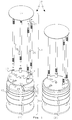
- Fig. 1 is comprised of Fig. 1(A) which shows an exploded perspective view of one specific embodiment of a wafer carrier comprised of the innovative wafer boat of the present invention and a conventional pedestal and Fig. 1(B) which shows the perspective view of the wafer carrier of Fig. 1(A) once assembled.
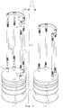
- Fig. 2 is comprised of Fig. 2(A) which shows an exploded perspective view of another embodiment of the wafer carrier of Fig. 1 wherein the conventional pedestal is modified to become a part of the innovative wafer boat and Fig. 2(B) which shows the perspective view of the wafer carrier of Fig. 2(A) once assembled.
- Fig. 1 shows an exploded view of a first embodiment of a heat treatment wafer carrier bearing numeral 10 according to the present invention.
- wafer carrier 10 is essentially comprised of two parts: the improved wafer boat 11 of the present invention and the heat insulation cylinder or pedestal 12, the wafer boat 11 being disposed atop the pedestal 12.
- the model of pedestal shown in Fig. 1 (A) is integral or unitary, i.e. all its constituting parts are welded together to form a single block structure.
- the construction of pedestal 12 is known per se and will not be described here any more.
- the improved wafer boat 11 of the present invention first includes two disc-shaped top and bottom plates 13 and 14 respectively that are spaced from each other of a predetermined distance. It further includes four support rods or rails 15, that are erected between said top and bottom plates 13 and 14 and are provided with slots or grooves 16 as standard to support the wafers (not shown). Slots 16 have a vertical width which is a little larger than the thickness of the wafers.
- the configuration shown in Fig. 1(A), i.e. with equal spacing between slots allows the reactant gas to flow uniformly, thereby permitting an excellent uniformity in the processing over the entire surface of the wafer. However, variable spacing could be envisioned as well.
- the wafers are loaded/unloaded in/out the slots 16 by the transfer arm of a handling robot (not shown) as standard.
- each plate and each support rod extremity are adapted so that the coupling therebetween is tight enough to produce an integral-like assembly but not too much to make it releasable.
- Different releasable connecting means can be envisioned to meet these contradictory objectives.
- each projection has a blind hole 18.
- These hollow projections are obtained by cutting an annular quartz glass rod with a standard diamond saw into pieces having the desired length.
- the length L of the projections 17 is 21 mm and the external diameter is 20 mm.
- These projections 17 are bored with a drilling machine to provide a central hole having an internal diameter D of 12 mm. It is recommended to have the projection length L greater than the internal diameter D for better precision of the fitting. A L/D ratio equal to about 2 appears adequate in most applications.
- the rod extremities have preferably a special design.
- its extremities are thinned, e.g. by grinding, to form a tip 19 with a plane shoulder at the rod/tip interface.
- the tips 19 are machined e.g. by grinding to have a length of 20 mm and a diameter just inferior to the internal diameter of the projections mentioned above.
- the adjustment blind hole/tip is perfectly defined by data 12g6/12H7 of norm ISO E02-350 to meet the two key objectives mentioned above: once the different parts constituting the wafer boat are combined, they must produce an unitary structure, i.e. all parts are firmly secured, but the coupling must not be too tight to allow easy assembling/disassembling of the wafer boat.
- tips 19 are not only matingly engageable in said blind holes 18 but they must fit snugly therewith. With this design, the tip shoulder acts a a stop member on the annular surface of the hollow projection.
- the above technique takes in account the fact that disc-shaped plates 13 and 14 are generally not thick enough (thickness in the range of 12 mm) to ensure proper fitting of the rod in a blind hole made therein. Should thicker plates be used (at the cost of an additional thermal inerty of the wafer boat), such a blind hole could be drilled in the plate to receive the rod extremity. In this case, the adjustment mentioned above should still be made for excellent fitting but on a few microns of the rod extremity external surface.
- the bottom plate 14 is provided with a centering hole 20, an alignment notch 21 and three pins 22 (only one is visible in Fig. 1(A)) are disposed at its lower surface as standard. As apparent from Fig.
- pedestal 12 is comprised of a plurality of circular plates.
- the surface of the pedestal top plate now referenced 23' is provided with two pegs.
- a first peg 24 (visible in Fig. 1(B)) fits with the centering hole 20 and the other peg 25 fits with the alignment notch 21 made in bottom plate 14 for centering and registration purposes respectively as known for those skilled in the art.
- Three grinded zones referenced 26 corresponding to pins 22 are also provided to top plate 23'.
- Fig. 1(B) shows the wafer boat 10 of Fig. 1(A) once assembled.
- the wafer boat 11 of Fig. 1 has high flexibility.
- the rods 16 with slots of different profiles and of different spacings.
- the two support rods 16 that are the most spaced can be provided with V-shaped slots (to facilitate the wafer load/unload operation) while the two others can be provided with U-shaped slots for a better holding of the wafers.
- the slot spacing may be choosen equal or variable, by assembling the adequate rods in-situ depending on specific process requirements.
- new materials such as silicon carbide, alumina, sintered ceramic or graphite have been recently used to fabricate wafer boats.
- the support rods can be made of SiC while the remaining parts of the wafer boat are made of quartz glass. If the wafers must be grounded during the heat treatment, all parts can be made of SiC except top plate 13. A good compromise between cost and reliability can now be obtained for the improved wafer boats of the present invention.
- Fig. 2 shows an exploded perspective view of another wafer carrier referenced 27 according to a second embodiment of the present invention.
- the wafer carrier 27 which is comprised of wafer boat 11' and pedestal 12' directly derives from wafer carrier 10 of Fig. 1, except in that a few changes have been made.
- the bottom plate 14 of wafer boat 10 has been eliminated.
- the top plate 23 of the pedestal 12 of Fig. 1 can be provided with hollow projections according to the teachings of the present invention. These projections are constructed and attached to the top plate now referenced 23' according to the above described technique.
- Another change may consist in the replacement of the top disc-shaped plate 13 by an arcuate member 28 that is provided with a plurality of apertured cylinders 29 which play the same role that projections 17.
- Fig. 2(B) shows the wafer carrier 27 of Fig. 2(A) once assembled.
- support rods could have a square section instead of a circular one, ... etc.
- the innovative wafer boats/carriers of the present invention are applicable to the handling of wafers in areas such as oxidation, diffusion, chemical vapor deposition, etching, cleaning and the like, all steps that are essential to the wafer batch thermal processing.
Landscapes
- Container, Conveyance, Adherence, Positioning, Of Wafer (AREA)
Priority Applications (1)
| Application Number | Priority Date | Filing Date | Title |
|---|---|---|---|
| EP96480105A EP0843338A1 (fr) | 1996-11-15 | 1996-11-15 | Une nacelle améliorée pour supporter des plaquettes semi-conductrices |
Applications Claiming Priority (1)
| Application Number | Priority Date | Filing Date | Title |
|---|---|---|---|
| EP96480105A EP0843338A1 (fr) | 1996-11-15 | 1996-11-15 | Une nacelle améliorée pour supporter des plaquettes semi-conductrices |
Publications (1)
| Publication Number | Publication Date |
|---|---|
| EP0843338A1 true EP0843338A1 (fr) | 1998-05-20 |
Family
ID=8225461
Family Applications (1)
| Application Number | Title | Priority Date | Filing Date |
|---|---|---|---|
| EP96480105A Withdrawn EP0843338A1 (fr) | 1996-11-15 | 1996-11-15 | Une nacelle améliorée pour supporter des plaquettes semi-conductrices |
Country Status (1)
| Country | Link |
|---|---|
| EP (1) | EP0843338A1 (fr) |
Cited By (13)
| Publication number | Priority date | Publication date | Assignee | Title |
|---|---|---|---|---|
| KR100410982B1 (ko) * | 2001-01-18 | 2003-12-18 | 삼성전자주식회사 | 반도체 제조장치용 보트 |
| US6799940B2 (en) | 2002-12-05 | 2004-10-05 | Tokyo Electron Limited | Removable semiconductor wafer susceptor |
| CN1332392C (zh) * | 1998-05-28 | 2007-08-15 | 诚实公司 | 复合基质载体 |
| DE102015111144A1 (de) * | 2015-07-09 | 2017-01-12 | Hanwha Q.CELLS GmbH | Vorrichtung zur paarweisen Aufnahme von Substraten |
| US10014199B2 (en) * | 2015-11-18 | 2018-07-03 | Tokyo Electron Limited | Wafer boat support table and heat treatment apparatus using the same |
| CN109082649A (zh) * | 2018-09-06 | 2018-12-25 | 深圳市捷佳伟创新能源装备股份有限公司 | 一种稳定镀膜的载片装置 |
| CN110993543A (zh) * | 2019-10-23 | 2020-04-10 | 深圳市拉普拉斯能源技术有限公司 | 新型方舟结构 |
| DE102015217132B4 (de) | 2014-09-19 | 2022-01-05 | Siconnex Customized Solutions Gmbh | Halterungssystem, Behandlungsvorrichtung und Beschickungsverfahren für scheibenförmige Objekte |
| CN114351256A (zh) * | 2020-10-13 | 2022-04-15 | 中国科学院微电子研究所 | 晶舟、拆装工具以及晶圆加工设备 |
| US20220254668A1 (en) * | 2021-02-08 | 2022-08-11 | Asm Ip Holding B.V. | Wafer boat |
| CN115172232A (zh) * | 2022-08-23 | 2022-10-11 | 北京北方华创微电子装备有限公司 | 一种晶舟和半导体工艺设备 |
| CN118166327A (zh) * | 2024-01-17 | 2024-06-11 | 无锡松煜科技有限公司 | 一种用于硼扩散过程的碳化硅桨装置 |
| WO2026015408A1 (fr) * | 2024-07-10 | 2026-01-15 | Globalwafers Co., Ltd. | Systèmes de transport d'une pluralité de structures semi-conductrices, nacelles à tranches et procédés de chauffage d'un ensemble de structures semi-conductrices |
Citations (3)
| Publication number | Priority date | Publication date | Assignee | Title |
|---|---|---|---|---|
| DE2422527A1 (de) * | 1974-05-09 | 1975-11-20 | Semikron Gleichrichterbau | Vorrichtung zum gleichzeitigen, beiderseitigen beschichten mehrerer halbleiterscheiben mit einem schutzlack |
| EP0100539A2 (fr) | 1982-07-30 | 1984-02-15 | Tecnisco Ltd. | Appareil assemblé pour supporter des pastilles semi-conductrices ou semblables |
| US5458688A (en) * | 1993-03-09 | 1995-10-17 | Tokyo Electron Kabushiki Kaisha | Heat treatment boat |
-
1996
- 1996-11-15 EP EP96480105A patent/EP0843338A1/fr not_active Withdrawn
Patent Citations (3)
| Publication number | Priority date | Publication date | Assignee | Title |
|---|---|---|---|---|
| DE2422527A1 (de) * | 1974-05-09 | 1975-11-20 | Semikron Gleichrichterbau | Vorrichtung zum gleichzeitigen, beiderseitigen beschichten mehrerer halbleiterscheiben mit einem schutzlack |
| EP0100539A2 (fr) | 1982-07-30 | 1984-02-15 | Tecnisco Ltd. | Appareil assemblé pour supporter des pastilles semi-conductrices ou semblables |
| US5458688A (en) * | 1993-03-09 | 1995-10-17 | Tokyo Electron Kabushiki Kaisha | Heat treatment boat |
Cited By (16)
| Publication number | Priority date | Publication date | Assignee | Title |
|---|---|---|---|---|
| CN1332392C (zh) * | 1998-05-28 | 2007-08-15 | 诚实公司 | 复合基质载体 |
| KR100410982B1 (ko) * | 2001-01-18 | 2003-12-18 | 삼성전자주식회사 | 반도체 제조장치용 보트 |
| US6799940B2 (en) | 2002-12-05 | 2004-10-05 | Tokyo Electron Limited | Removable semiconductor wafer susceptor |
| DE102015217132B4 (de) | 2014-09-19 | 2022-01-05 | Siconnex Customized Solutions Gmbh | Halterungssystem, Behandlungsvorrichtung und Beschickungsverfahren für scheibenförmige Objekte |
| DE102015111144A1 (de) * | 2015-07-09 | 2017-01-12 | Hanwha Q.CELLS GmbH | Vorrichtung zur paarweisen Aufnahme von Substraten |
| US10014199B2 (en) * | 2015-11-18 | 2018-07-03 | Tokyo Electron Limited | Wafer boat support table and heat treatment apparatus using the same |
| CN109082649A (zh) * | 2018-09-06 | 2018-12-25 | 深圳市捷佳伟创新能源装备股份有限公司 | 一种稳定镀膜的载片装置 |
| CN110993543B (zh) * | 2019-10-23 | 2023-07-04 | 拉普拉斯新能源科技股份有限公司 | 方舟结构 |
| CN110993543A (zh) * | 2019-10-23 | 2020-04-10 | 深圳市拉普拉斯能源技术有限公司 | 新型方舟结构 |
| CN114351256A (zh) * | 2020-10-13 | 2022-04-15 | 中国科学院微电子研究所 | 晶舟、拆装工具以及晶圆加工设备 |
| US20220254668A1 (en) * | 2021-02-08 | 2022-08-11 | Asm Ip Holding B.V. | Wafer boat |
| CN114914180A (zh) * | 2021-02-08 | 2022-08-16 | Asm Ip私人控股有限公司 | 晶片舟 |
| US11869786B2 (en) * | 2021-02-08 | 2024-01-09 | Asm Ip Holding B.V. | Wafer boat |
| CN115172232A (zh) * | 2022-08-23 | 2022-10-11 | 北京北方华创微电子装备有限公司 | 一种晶舟和半导体工艺设备 |
| CN118166327A (zh) * | 2024-01-17 | 2024-06-11 | 无锡松煜科技有限公司 | 一种用于硼扩散过程的碳化硅桨装置 |
| WO2026015408A1 (fr) * | 2024-07-10 | 2026-01-15 | Globalwafers Co., Ltd. | Systèmes de transport d'une pluralité de structures semi-conductrices, nacelles à tranches et procédés de chauffage d'un ensemble de structures semi-conductrices |
Similar Documents
| Publication | Publication Date | Title |
|---|---|---|
| EP0843338A1 (fr) | Une nacelle améliorée pour supporter des plaquettes semi-conductrices | |
| US6065615A (en) | Vertical wafer boat | |
| US20020113027A1 (en) | Retainer for use in heat treatment of substrate, substrate heat treatment equipment, and method of manufacturing the retainer | |
| US5584936A (en) | Susceptor for semiconductor wafer processing | |
| KR100880410B1 (ko) | 웨이퍼 홀딩 장치 | |
| US6530994B1 (en) | Platform for supporting a semiconductor substrate and method of supporting a substrate during rapid high temperature processing | |
| US5580388A (en) | Multi-layer susceptor for rapid thermal process reactors | |
| US6092981A (en) | Modular substrate cassette | |
| US5820686A (en) | Multi-layer susceptor for rapid thermal process reactors | |
| US6056123A (en) | Semiconductor wafer carrier having the same composition as the wafers | |
| US5174660A (en) | Shaped part comprising a metallic member and a ceramic member | |
| TW201803005A (zh) | 用於高溫製程之基板支撐組件 | |
| US6799940B2 (en) | Removable semiconductor wafer susceptor | |
| JP2012182464A (ja) | 基板支持組立体のためのシリコンカーバイドスリーブ | |
| EP0506052A1 (fr) | Gabarit à base du carbure de silicium | |
| TWI904130B (zh) | 基板處理系統、其氣體分配板及氣體分配組件 | |
| US8323411B2 (en) | Semiconductor workpiece apparatus | |
| US6276592B1 (en) | Process for the production of a holding device for semiconductor disks and holding device produced by this process | |
| JPS59232994A (ja) | 気相成長装置 | |
| KR20230062184A (ko) | 웨이퍼 보트 | |
| JP2002261035A (ja) | 縦型熱処理装置及び縦型熱処理用基板保持具固定部材 | |
| US5711808A (en) | Boat for vertical diffusion furnace | |
| JPH06224281A (ja) | ウエハ移載用治具 | |
| KR20010035982A (ko) | 반도체 제조 설비용 서셉터 시스템 | |
| CN120998868A (zh) | 承载装置及半导体工艺设备 |
Legal Events
| Date | Code | Title | Description |
|---|---|---|---|
| PUAI | Public reference made under article 153(3) epc to a published international application that has entered the european phase |
Free format text: ORIGINAL CODE: 0009012 |
|
| 17P | Request for examination filed |
Effective date: 19971114 |
|
| AK | Designated contracting states |
Kind code of ref document: A1 Designated state(s): DE FR GB |
|
| AKX | Designation fees paid |
Free format text: DE FR GB |
|
| RBV | Designated contracting states (corrected) |
Designated state(s): DE FR GB |
|
| 17Q | First examination report despatched |
Effective date: 19991207 |
|
| GRAG | Despatch of communication of intention to grant |
Free format text: ORIGINAL CODE: EPIDOS AGRA |
|
| GRAG | Despatch of communication of intention to grant |
Free format text: ORIGINAL CODE: EPIDOS AGRA |
|
| GRAH | Despatch of communication of intention to grant a patent |
Free format text: ORIGINAL CODE: EPIDOS IGRA |
|
| STAA | Information on the status of an ep patent application or granted ep patent |
Free format text: STATUS: THE APPLICATION IS DEEMED TO BE WITHDRAWN |
|
| 18D | Application deemed to be withdrawn |
Effective date: 20020604 |