EP0843349A1 - Verfahren zur Herstellung eines NPN-Transistors mit einer geringen Fläche - Google Patents
Verfahren zur Herstellung eines NPN-Transistors mit einer geringen Fläche Download PDFInfo
- Publication number
- EP0843349A1 EP0843349A1 EP97410129A EP97410129A EP0843349A1 EP 0843349 A1 EP0843349 A1 EP 0843349A1 EP 97410129 A EP97410129 A EP 97410129A EP 97410129 A EP97410129 A EP 97410129A EP 0843349 A1 EP0843349 A1 EP 0843349A1
- Authority
- EP
- European Patent Office
- Prior art keywords
- layer
- mask
- polycrystalline silicon
- base
- silicon
- Prior art date
- Legal status (The legal status is an assumption and is not a legal conclusion. Google has not performed a legal analysis and makes no representation as to the accuracy of the status listed.)
- Withdrawn
Links
- 238000000034 method Methods 0.000 title claims description 5
- 239000010410 layer Substances 0.000 claims abstract description 87
- 229910021420 polycrystalline silicon Inorganic materials 0.000 claims abstract description 38
- 239000011241 protective layer Substances 0.000 claims abstract description 10
- VYPSYNLAJGMNEJ-UHFFFAOYSA-N Silicium dioxide Chemical compound O=[Si]=O VYPSYNLAJGMNEJ-UHFFFAOYSA-N 0.000 claims description 13
- 238000002513 implantation Methods 0.000 claims description 12
- 238000004519 manufacturing process Methods 0.000 claims description 12
- HQVNEWCFYHHQES-UHFFFAOYSA-N silicon nitride Chemical compound N12[Si]34N5[Si]62N3[Si]51N64 HQVNEWCFYHHQES-UHFFFAOYSA-N 0.000 claims description 12
- 229910052581 Si3N4 Inorganic materials 0.000 claims description 11
- 229910052814 silicon oxide Inorganic materials 0.000 claims description 11
- 125000006850 spacer group Chemical group 0.000 claims description 11
- 238000000151 deposition Methods 0.000 claims description 6
- 230000015572 biosynthetic process Effects 0.000 claims description 4
- 238000005530 etching Methods 0.000 claims description 3
- 238000000137 annealing Methods 0.000 claims description 2
- 230000001590 oxidative effect Effects 0.000 claims description 2
- 238000009792 diffusion process Methods 0.000 description 9
- XUIMIQQOPSSXEZ-UHFFFAOYSA-N Silicon Chemical compound [Si] XUIMIQQOPSSXEZ-UHFFFAOYSA-N 0.000 description 7
- 229910052710 silicon Inorganic materials 0.000 description 7
- 239000010703 silicon Substances 0.000 description 7
- 239000002019 doping agent Substances 0.000 description 6
- 230000003071 parasitic effect Effects 0.000 description 3
- ZOXJGFHDIHLPTG-UHFFFAOYSA-N Boron Chemical compound [B] ZOXJGFHDIHLPTG-UHFFFAOYSA-N 0.000 description 2
- 229910052785 arsenic Inorganic materials 0.000 description 2
- 229910052796 boron Inorganic materials 0.000 description 2
- 230000008021 deposition Effects 0.000 description 2
- 238000002955 isolation Methods 0.000 description 2
- 238000005304 joining Methods 0.000 description 2
- 150000004767 nitrides Chemical class 0.000 description 2
- 239000000758 substrate Substances 0.000 description 2
- FARHYDJOXLCMRP-UHFFFAOYSA-N 2-[4-[2-(2,3-dihydro-1H-inden-2-ylamino)pyrimidin-5-yl]-1-[2-oxo-2-(2,4,6,7-tetrahydrotriazolo[4,5-c]pyridin-5-yl)ethyl]pyrazol-3-yl]oxyacetic acid Chemical group C1C(CC2=CC=CC=C12)NC1=NC=C(C=N1)C=1C(=NN(C=1)CC(N1CC2=C(CC1)NN=N2)=O)OCC(=O)O FARHYDJOXLCMRP-UHFFFAOYSA-N 0.000 description 1
- RQNWIZPPADIBDY-UHFFFAOYSA-N arsenic atom Chemical compound [As] RQNWIZPPADIBDY-UHFFFAOYSA-N 0.000 description 1
- 230000015556 catabolic process Effects 0.000 description 1
- 239000003795 chemical substances by application Substances 0.000 description 1
- 238000005520 cutting process Methods 0.000 description 1
- 238000005538 encapsulation Methods 0.000 description 1
- 238000009413 insulation Methods 0.000 description 1
- 239000012212 insulator Substances 0.000 description 1
- 229910021421 monocrystalline silicon Inorganic materials 0.000 description 1
- 230000003647 oxidation Effects 0.000 description 1
- 238000007254 oxidation reaction Methods 0.000 description 1
- 238000004151 rapid thermal annealing Methods 0.000 description 1
- 239000007787 solid Substances 0.000 description 1
- 230000007704 transition Effects 0.000 description 1
- 238000011282 treatment Methods 0.000 description 1
Images


Classifications
-
- H—ELECTRICITY
- H10—SEMICONDUCTOR DEVICES; ELECTRIC SOLID-STATE DEVICES NOT OTHERWISE PROVIDED FOR
- H10D—INORGANIC ELECTRIC SEMICONDUCTOR DEVICES
- H10D10/00—Bipolar junction transistors [BJT]
- H10D10/01—Manufacture or treatment
- H10D10/051—Manufacture or treatment of vertical BJTs
-
- H—ELECTRICITY
- H10—SEMICONDUCTOR DEVICES; ELECTRIC SOLID-STATE DEVICES NOT OTHERWISE PROVIDED FOR
- H10D—INORGANIC ELECTRIC SEMICONDUCTOR DEVICES
- H10D10/00—Bipolar junction transistors [BJT]
- H10D10/40—Vertical BJTs
Definitions
- the present invention relates to the field of circuits integrated and more particularly the manufacture of a transistor NPN.
- This NPN transistor is formed in an epitaxial layer 2 surmounting a buried layer 3 formed in a silicon substrate P type (not shown). The transistor is formed in a window in a thick oxide layer 5.
- References 21 and 22 denote thin layers of silicon oxide and silicon nitride which are used to protect other integrated circuit elements (such as CMOS transistors) during the fabrication of the bipolar transistor.
- Reference 23 denotes a portion of a layer of doped polycrystalline silicon P type called basic polycrystalline silicon since it is from this layer of silicon that is formed the diffusion of base contact 32.
- the polycrystalline silicon layer 23 is coated with a layer of encapsulating silicon oxide 24. A transmitter-base central opening is formed in all layers 23 and 24.
- a thin layer of silicon oxide 31 covers the sides of the polycrystalline silicon layer 23 and the bottom of the opening.
- an implantation is carried out high energy type N for training of a sub-collector region of selected doping level.
- the walls of the emitter-base opening are coated with a layer of silicon nitride 44.
- Lateral spacers of silicon polycrystalline 43 are formed on the sides of the opening.
- an implantation intrinsic base 33 Before formation of the silicon nitride region 44 and polycrystalline silicon spacers 43 is formed an implantation intrinsic base 33.
- the layer of polycrystalline silicon 46 is coated with a layer encapsulation oxide 47.
- the entire structure is coated of an isolation and planarization layer 51 through which are formed transmitter contact openings 55 joining the polycrystalline silicon layer 46 and contact base 56 joining the polycrystalline silicon layer 23.
- a collector contact (not shown) is made by via deep N-type diffusion to the layer buried 3.
- This transistor is circularly symmetrical, the emitter being central and the basic polycrystalline silicon being in ring around this transmitter.
- An object of the present invention is to provide a NPN transistor of the same general type as that of Figure 1 but whose topology is modified so that it can have a dimension minimal.
- Another object of the present invention is to provide an NPN transistor whose parasitic capacities are reduced and which is therefore likely to operate at frequencies high.
- the present invention provides an NPN transistor whose base and emitter are formed at the interior of a window defined in a thick oxide according to a first substantially rectangular mask. At least part of the area defined by the first mask is covered with a layer of polycrystalline silicon, preferably along one side of this first mask; a basic contact area is formed under this polycrystalline silicon zone; the other three sides of the emitter-base area are delimited by a protective layer, an intrinsic base area being formed in the opening thus defined then an emitter area covered with a layer of N-doped polycrystalline silicon.
- the present invention also provides a method of fabrication of an NPN transistor in an epitaxial layer of the type N including the steps of delimiting a window in a thick oxide layer, according to a first mask substantially rectangular; apply a protective layer and remove it inside an opening defined by a second mask of generally internal to the first mask and overflowing on one side of it; deposit a first layer of polycrystalline silicon and a layer of silicon oxide and open it inside of a contour defined by a third mask including a common part of the first two masks; anneal oxidative thermal; proceed to a type P training establishment intrinsic base; deposit a nitride layer of silicon and a second layer of polycrystalline silicon, etch the polycrystalline silicon layer anisotropically to leave only spacers in place along the sides of the opening defined by the third mask, and eliminate the silicon nitride layer where it is not protected by the spacers; proceed with a strong N-type implantation energy to form a collector region; and file a polycrystalline silicon layer of type N emitter
- the protective layer comprises a layer of silicon oxide and a layer of silicon nitride.
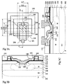
- FIGS 2A to 2C show an NPN transistor according to the present invention at an intermediate manufacturing stage.
- the technological steps are much the same as those described in relation to Figure 1 but the topology and the relative positions of the masks are distinct.
- the NPN transistor is formed in an N-type epitaxial layer 101 formed on a P-type substrate 102, a buried heavily doped N-type (N + ) layer 103 being disposed under the active parts of the NPN transistor.
- the lateral insulation of the NPN transistors from each other and from other elements of the integrated circuit is done by isolation walls made up of P-type diffusions extending over the entire thickness of the epitaxial layer 101.
- the structure emitter-base is formed inside a window delimited by a mask of substantially rectangular shape 200 in a thick oxide layer 105.
- a protective layer 121-122 for example made up a layer of silicon oxide 121 and a layer of silicon nitride 122, is deposited on the structure.
- This protective layer is open along the outline of a mask 201 also of substantially rectangular shape.
- the mask 201 is arranged inside three sides of the mask 200 and overflows with respect to this mask 200 on the fourth side.
- a layer of "basic" 123 polycrystalline silicon, doped with type P by implantation after deposition, and a layer of encapsulating silicon oxide 124 are successively deposited.
- An opening is formed in layers 123-124 along the outline of a substantially rectangular mask 202 of which three sides are outside the contours of the masks 200 and 201 and the fourth side of which intersects these masks 200 and 201.
- the part of the mask 202 projecting from the mask 200 is opposite the part of the mask 201 projecting from this mask 200.
- the layer of doped polycrystalline silicon type P 123 is in contact with the upper surface of the epitaxial layer 101 in a portion which corresponds to the area hatched 232 in FIG. 2A.
- the next step consists of implanting a P-type dopant intended for the formation of the intrinsic base region 133.
- This intrinsic base is preferably implanted with low energy boron (for example 10 13 atoms / cm 2 under 5 keV).
- low energy boron for example 10 13 atoms / cm 2 under 5 keV.
- the dopants cannot pass through either the protective layer 121-122 or, a fortiori, the whole of the polycrystalline silicon layer 123 and the silicon oxide layer 124.
- the implantation is therefore limited. to an "intrinsic base opening" 233 defined by the intersection of the masks 200 and 202.
- this implantation is carried out under an oblique incidence (for example at an angle of 7 °) to make the dopant penetrate beyond the outline of the opening.
- a layer of nitride is then deposited. silicon and a polycrystalline silicon layer.
- the layer of polycrystalline silicon is etched over its entire thickness of anisotropic way to leave only spacers in place 143 on the sides of the openings formed in layers 123 and 124.
- the entire apparent surface of the layer of etching is etched. silicon nitride that has just been deposited so this layer of silicon nitride stays in place only in portions 144 enclosed by the spacers 143.
- Transmitter opening the outline of which is designated by the reference 230 in the top view of FIG. 3A.
- This opening is covered only with the thin layer of silicon oxide 131 as seen in Figures 2B and 2C.
- the surface of this opening is defined by the intersection of the masks 200 and 202 (intrinsic base opening), reduced on the edge of the mask 202 of the width of the spacer 143.
- N-type dopant is then implanted to define the collector 130 of the NPN transistor.
- This implantation is carried out at medium dose and at high energy (for example 10 12 to 10 14 atoms / cm 2 at 500 keV).
- the result of this implementation appears in Figures 2B and 2C. It will be noted that, due to the topology of the various layers previously etched, this layout extends under the emitter opening 230, and beyond this opening but not under the base contact region 223 which is masked by all the layers 123 and 124 and the spacer 143. An effective collector region 130 is thus obtained of limited lateral extent, substantially equal to that of the intrinsic base. This contributes to obtaining an NPN transistor of low parasitic capacity between collector and extrinsic base.
- the layout is optimized (for example, by successive layouts) so that the profile of the collector provides the best possible compromise between, on the one hand, the collector resistance and the transit time in this collector and, on the other hand, obtaining sufficiently high breakdown voltages emitter-collector (typically 4 volts) and base-collector and of a low capacity base-collector.
- this collector layout makes it possible to choose beforehand an epitaxial layer 2 of doping and thickness suitable for optimizing CMOS transistors formed on the same chip and then independently optimizing the characteristics of the NPN transistor.
- the epitaxial layer 101 may be thicker than if it were to serve directly as a collector layer of the NPN transistor.
- the buried layer 3 will be extended to one side or on the other side of the structure to come into contact with a box N type allowing a collector contact resumption, as this is usual.
- the use of this technique and this topology makes it possible to obtain an NPN transistor of minimum dimension.
- the minimum dimension of an opening in a mask is 0.3 ⁇ m
- the hatched area designated by the reference 230 of effective transmitter contact may have dimensions of the order of 0.3 x 0.3 ⁇ m, that is to say that the effective opening of the transmitter has an area of the order of 0.1 ⁇ m 2 .
- the transistor according to the invention has many advantages.
- the surface of the emitter or useful surface is of the order of 0.2 ⁇ m 2 and the active surface (surface of the opening in the thick oxide) is 2 ⁇ m 2 .
- the useful surface goes from 0.2 to 0.1 ⁇ m 2 .
- the surface of the intrinsic transistor is therefore reduced by a factor of 2. It follows that the transistor will have the same transition frequency for a current 2 times lower and therefore a reduced consumption.
- the parasitic parts of the transistor go from 1.7 to 0.1 ⁇ 2 .
- the extrinsic base-collector capacity will be reduced accordingly.
Landscapes
- Bipolar Transistors (AREA)
Applications Claiming Priority (2)
| Application Number | Priority Date | Filing Date | Title |
|---|---|---|---|
| FR9614408A FR2756099B1 (fr) | 1996-11-19 | 1996-11-19 | Procede de fabrication d'un transistor npn de surface minimale |
| FR9614408 | 1996-11-19 |
Publications (1)
| Publication Number | Publication Date |
|---|---|
| EP0843349A1 true EP0843349A1 (de) | 1998-05-20 |
Family
ID=9497992
Family Applications (1)
| Application Number | Title | Priority Date | Filing Date |
|---|---|---|---|
| EP97410129A Withdrawn EP0843349A1 (de) | 1996-11-19 | 1997-11-18 | Verfahren zur Herstellung eines NPN-Transistors mit einer geringen Fläche |
Country Status (4)
| Country | Link |
|---|---|
| US (1) | US5880000A (de) |
| EP (1) | EP0843349A1 (de) |
| JP (1) | JP3161395B2 (de) |
| FR (1) | FR2756099B1 (de) |
Cited By (1)
| Publication number | Priority date | Publication date | Assignee | Title |
|---|---|---|---|---|
| EP0993033A1 (de) * | 1998-10-06 | 2000-04-12 | STMicroelectronics S.r.l. | Gate-Isolierungsstruktur für Leistungs-MOS-Transistor und Herstellungsverfahren dafür |
Families Citing this family (4)
| Publication number | Priority date | Publication date | Assignee | Title |
|---|---|---|---|---|
| FR2756100B1 (fr) | 1996-11-19 | 1999-02-12 | Sgs Thomson Microelectronics | Transistor bipolaire a emetteur inhomogene dans un circuit integre bicmos |
| FR2756101B1 (fr) * | 1996-11-19 | 1999-02-12 | Sgs Thomson Microelectronics | Procede de fabrication d'un transistor npn dans une technologie bicmos |
| FR2756103B1 (fr) * | 1996-11-19 | 1999-05-14 | Sgs Thomson Microelectronics | Fabrication de circuits integres bipolaires/cmos et d'un condensateur |
| FR2790867B1 (fr) * | 1999-03-12 | 2001-11-16 | St Microelectronics Sa | Procede de fabrication de transistor bipolaire |
Citations (1)
| Publication number | Priority date | Publication date | Assignee | Title |
|---|---|---|---|---|
| US5439832A (en) * | 1993-06-04 | 1995-08-08 | Fujitsu Limited | Method for fabricating semiconductor device |
Family Cites Families (2)
| Publication number | Priority date | Publication date | Assignee | Title |
|---|---|---|---|---|
| US4215418A (en) * | 1978-06-30 | 1980-07-29 | Trw Inc. | Integrated digital multiplier circuit using current mode logic |
| US4276543A (en) * | 1979-03-19 | 1981-06-30 | Trw Inc. | Monolithic triple diffusion analog to digital converter |
-
1996
- 1996-11-19 FR FR9614408A patent/FR2756099B1/fr not_active Expired - Fee Related
-
1997
- 1997-11-13 US US08/969,996 patent/US5880000A/en not_active Expired - Lifetime
- 1997-11-18 EP EP97410129A patent/EP0843349A1/de not_active Withdrawn
- 1997-11-19 JP JP33375897A patent/JP3161395B2/ja not_active Expired - Fee Related
Patent Citations (1)
| Publication number | Priority date | Publication date | Assignee | Title |
|---|---|---|---|---|
| US5439832A (en) * | 1993-06-04 | 1995-08-08 | Fujitsu Limited | Method for fabricating semiconductor device |
Cited By (3)
| Publication number | Priority date | Publication date | Assignee | Title |
|---|---|---|---|---|
| EP0993033A1 (de) * | 1998-10-06 | 2000-04-12 | STMicroelectronics S.r.l. | Gate-Isolierungsstruktur für Leistungs-MOS-Transistor und Herstellungsverfahren dafür |
| US6365931B1 (en) | 1998-10-06 | 2002-04-02 | Stmicroelectronics S.R.L. | Gate insulating structure for power devices, and related manufacturing process |
| US6756259B2 (en) | 1998-10-06 | 2004-06-29 | Stmicroelectronics S.R.L. | Gate insulating structure for power devices, and related manufacturing process |
Also Published As
| Publication number | Publication date |
|---|---|
| JPH10163221A (ja) | 1998-06-19 |
| FR2756099A1 (fr) | 1998-05-22 |
| FR2756099B1 (fr) | 1999-02-12 |
| US5880000A (en) | 1999-03-09 |
| JP3161395B2 (ja) | 2001-04-25 |
Similar Documents
| Publication | Publication Date | Title |
|---|---|---|
| EP0843354B1 (de) | Herstellung von integrierten bipolaren/CMOS-Schaltkreisen | |
| EP3273483B1 (de) | Herstellungsverfahren eines bipolaren transistors vom typ pnp, parallel zu einem bipolaren transistor vom typ npn, sowie mos transistoren mit einem n- und einem p-kanal | |
| US4707456A (en) | Method of making a planar structure containing MOS and bipolar transistors | |
| EP0851488B1 (de) | Verfahren zur Herstellung eines Bipolartransistors mit dielektrischer Isolation | |
| EP1406307A1 (de) | Integrierte Schaltung mit einer hochleitenden begrabenen Schicht | |
| EP0843350B1 (de) | Bipolartransistor mit einem nicht homogenen Emitter in einer BICMOS integrierter Schaltung | |
| EP0843355A1 (de) | Herstellung von integrierten Bipolar-/CMOS-Schaltkreisen und einem Kondensator | |
| EP0135401B1 (de) | Verfahren zur Herstellung isolierter Halbleiterkomponenten in einem Halbleitersubstrat | |
| EP0414618B1 (de) | Dünnfilm-MOS-Transistor, bei dem die Kanalzone mit der Source verbunden ist, und Verfahren zur Herstellung | |
| EP0843351A1 (de) | Verfahren zur Herstellung eines NPN-Transistors in einer BICMOS Technologie | |
| EP1006573B1 (de) | Herstellungsverfahren für integrierte BiCMOS Schaltkreise auf einem gewöhnlichen CMOS Substrat | |
| EP0843349A1 (de) | Verfahren zur Herstellung eines NPN-Transistors mit einer geringen Fläche | |
| EP0849792A1 (de) | BiCMOS-Verfahren mit Kondensator | |
| EP0517623B1 (de) | Transistor mit einer vorbestimmten Stromverstärkung in einer integrierten Bipolarschaltung | |
| EP1146561A1 (de) | Herstellungverfahren für einen Bipolartransistor | |
| EP0949666B1 (de) | Basis-Emitter Gebiet von einem Submikrometer-Bipolartransistor | |
| EP0872893A1 (de) | PNP-Lateraltransistor in CMOS-Technologie | |
| EP0848429B1 (de) | Bipolarer Transistor mit Wannenisolierung | |
| US6465318B1 (en) | Bipolar transistor and method for producing same | |
| EP1146554A1 (de) | Verfahren zur Herstellung vergrabener Schichten | |
| FR3069702A1 (fr) | Procede de fabrication simultanee de transistors soi et de transistors sur substrat massif | |
| EP0024222B1 (de) | Verfahren zur Herstellung eines Feldeffekttransistors mit selbstjustiertem SCHOTTKY-Gate | |
| EP0401135A1 (de) | Verfahren zum gleichzeitigen Herstellen von N-Kanal-MOS-Transistoren und vertikalen PNP-Bipolartransistoren | |
| FR2516309A1 (fr) | Procede de fabrication d'un inverseur cmos forme de deux transistors empiles et auto-alignes par rapport a la grille de l'inverseur | |
| EP0872881A1 (de) | Verfahren zur Herstellung eines Bipolartransistors und seines Emitterkontakts |
Legal Events
| Date | Code | Title | Description |
|---|---|---|---|
| PUAI | Public reference made under article 153(3) epc to a published international application that has entered the european phase |
Free format text: ORIGINAL CODE: 0009012 |
|
| AK | Designated contracting states |
Kind code of ref document: A1 Designated state(s): DE FR CH DE DK ES FI FR GB GR IE IT LI LU MC NL PT SE |
|
| AX | Request for extension of the european patent |
Free format text: AL;LT;LV;MK;RO;SI |
|
| 17P | Request for examination filed |
Effective date: 19981102 |
|
| AKX | Designation fees paid |
Free format text: AT BE CH DE DK ES FI FR GB GR IE IT LI LU MC NL PT SE |
|
| AXX | Extension fees paid |
Free format text: AL;LT;LV;MK;RO;SI |
|
| RAP3 | Party data changed (applicant data changed or rights of an application transferred) |
Owner name: STMICROELECTRONICS S.A. |
|
| RBV | Designated contracting states (corrected) |
Designated state(s): DE FR GB IT |
|
| RAP1 | Party data changed (applicant data changed or rights of an application transferred) |
Owner name: STMICROELECTRONICS S.A. |
|
| STAA | Information on the status of an ep patent application or granted ep patent |
Free format text: STATUS: THE APPLICATION IS DEEMED TO BE WITHDRAWN |
|
| 18D | Application deemed to be withdrawn |
Effective date: 20040531 |