EP0844510A1 - Ferroelektrische Flüssigkristallvorrichtung und Verfahren zur Behandlung derselben - Google Patents
Ferroelektrische Flüssigkristallvorrichtung und Verfahren zur Behandlung derselben Download PDFInfo
- Publication number
- EP0844510A1 EP0844510A1 EP98100899A EP98100899A EP0844510A1 EP 0844510 A1 EP0844510 A1 EP 0844510A1 EP 98100899 A EP98100899 A EP 98100899A EP 98100899 A EP98100899 A EP 98100899A EP 0844510 A1 EP0844510 A1 EP 0844510A1
- Authority
- EP
- European Patent Office
- Prior art keywords
- liquid crystal
- cell
- degrees
- ferroelectric liquid
- angle
- Prior art date
- Legal status (The legal status is an assumption and is not a legal conclusion. Google has not performed a legal analysis and makes no representation as to the accuracy of the status listed.)
- Withdrawn
Links
- 239000005262 ferroelectric liquid crystals (FLCs) Substances 0.000 title claims abstract description 82
- 238000000034 method Methods 0.000 title description 19
- 239000004973 liquid crystal related substance Substances 0.000 claims abstract description 140
- 239000000758 substrate Substances 0.000 claims abstract description 130
- 239000004990 Smectic liquid crystal Substances 0.000 claims abstract description 51
- 238000002441 X-ray diffraction Methods 0.000 claims abstract description 32
- 230000005684 electric field Effects 0.000 claims abstract description 22
- 210000004027 cell Anatomy 0.000 claims description 146
- 210000002858 crystal cell Anatomy 0.000 claims description 22
- 239000011521 glass Substances 0.000 claims description 21
- 230000010287 polarization Effects 0.000 claims description 10
- 239000004642 Polyimide Substances 0.000 claims description 8
- 229920001721 polyimide Polymers 0.000 claims description 8
- 229920000642 polymer Polymers 0.000 claims description 8
- 230000002269 spontaneous effect Effects 0.000 claims description 8
- AMGQUBHHOARCQH-UHFFFAOYSA-N indium;oxotin Chemical compound [In].[Sn]=O AMGQUBHHOARCQH-UHFFFAOYSA-N 0.000 claims description 5
- RYGMFSIKBFXOCR-UHFFFAOYSA-N Copper Chemical compound [Cu] RYGMFSIKBFXOCR-UHFFFAOYSA-N 0.000 claims description 4
- 229910052802 copper Inorganic materials 0.000 claims description 4
- 239000010949 copper Substances 0.000 claims description 4
- 238000005070 sampling Methods 0.000 claims description 4
- 230000003287 optical effect Effects 0.000 claims description 3
- 238000001816 cooling Methods 0.000 abstract description 16
- 230000003247 decreasing effect Effects 0.000 abstract description 2
- 230000003252 repetitive effect Effects 0.000 abstract description 2
- 238000005259 measurement Methods 0.000 description 19
- 230000008859 change Effects 0.000 description 18
- 230000000052 comparative effect Effects 0.000 description 12
- 238000004040 coloring Methods 0.000 description 11
- 230000007547 defect Effects 0.000 description 11
- 230000007704 transition Effects 0.000 description 10
- VYPSYNLAJGMNEJ-UHFFFAOYSA-N Silicium dioxide Chemical compound O=[Si]=O VYPSYNLAJGMNEJ-UHFFFAOYSA-N 0.000 description 8
- 239000013078 crystal Substances 0.000 description 8
- 239000000203 mixture Substances 0.000 description 8
- 230000000717 retained effect Effects 0.000 description 7
- 230000032683 aging Effects 0.000 description 6
- 230000008033 biological extinction Effects 0.000 description 6
- 238000004544 sputter deposition Methods 0.000 description 5
- CIWBSHSKHKDKBQ-JLAZNSOCSA-N Ascorbic acid Chemical compound OC[C@H](O)[C@H]1OC(=O)C(O)=C1O CIWBSHSKHKDKBQ-JLAZNSOCSA-N 0.000 description 4
- CZPWVGJYEJSRLH-UHFFFAOYSA-N Pyrimidine Chemical compound C1=CN=CN=C1 CZPWVGJYEJSRLH-UHFFFAOYSA-N 0.000 description 4
- GWEVSGVZZGPLCZ-UHFFFAOYSA-N Titan oxide Chemical compound O=[Ti]=O GWEVSGVZZGPLCZ-UHFFFAOYSA-N 0.000 description 4
- 238000005452 bending Methods 0.000 description 4
- 238000010438 heat treatment Methods 0.000 description 4
- BPUBBGLMJRNUCC-UHFFFAOYSA-N oxygen(2-);tantalum(5+) Chemical compound [O-2].[O-2].[O-2].[O-2].[O-2].[Ta+5].[Ta+5] BPUBBGLMJRNUCC-UHFFFAOYSA-N 0.000 description 4
- 239000000377 silicon dioxide Substances 0.000 description 4
- 229910001936 tantalum oxide Inorganic materials 0.000 description 4
- OXPDQFOKSZYEMJ-UHFFFAOYSA-N 2-phenylpyrimidine Chemical compound C1=CC=CC=C1C1=NC=CC=N1 OXPDQFOKSZYEMJ-UHFFFAOYSA-N 0.000 description 3
- 239000004952 Polyamide Substances 0.000 description 3
- 239000002253 acid Substances 0.000 description 3
- 238000010586 diagram Methods 0.000 description 3
- 238000002474 experimental method Methods 0.000 description 3
- 229920002647 polyamide Polymers 0.000 description 3
- YCKRFDGAMUMZLT-UHFFFAOYSA-N Fluorine atom Chemical compound [F] YCKRFDGAMUMZLT-UHFFFAOYSA-N 0.000 description 2
- SECXISVLQFMRJM-UHFFFAOYSA-N N-Methylpyrrolidone Chemical compound CN1CCCC1=O SECXISVLQFMRJM-UHFFFAOYSA-N 0.000 description 2
- 239000011324 bead Substances 0.000 description 2
- 230000005540 biological transmission Effects 0.000 description 2
- 230000003098 cholesteric effect Effects 0.000 description 2
- 239000011248 coating agent Substances 0.000 description 2
- 238000000576 coating method Methods 0.000 description 2
- 229910052681 coesite Inorganic materials 0.000 description 2
- 229910052906 cristobalite Inorganic materials 0.000 description 2
- 229910052731 fluorine Inorganic materials 0.000 description 2
- 239000011737 fluorine Substances 0.000 description 2
- 230000003993 interaction Effects 0.000 description 2
- 239000000463 material Substances 0.000 description 2
- 230000007246 mechanism Effects 0.000 description 2
- 230000000704 physical effect Effects 0.000 description 2
- 239000002243 precursor Substances 0.000 description 2
- 230000002441 reversible effect Effects 0.000 description 2
- 229910052682 stishovite Inorganic materials 0.000 description 2
- PBCFLUZVCVVTBY-UHFFFAOYSA-N tantalum pentoxide Inorganic materials O=[Ta](=O)O[Ta](=O)=O PBCFLUZVCVVTBY-UHFFFAOYSA-N 0.000 description 2
- 238000012360 testing method Methods 0.000 description 2
- 229910052905 tridymite Inorganic materials 0.000 description 2
- 238000004383 yellowing Methods 0.000 description 2
- 229920000265 Polyparaphenylene Polymers 0.000 description 1
- 230000002411 adverse Effects 0.000 description 1
- 230000015572 biosynthetic process Effects 0.000 description 1
- 239000000470 constituent Substances 0.000 description 1
- 230000006866 deterioration Effects 0.000 description 1
- 230000000694 effects Effects 0.000 description 1
- 230000005520 electrodynamics Effects 0.000 description 1
- 238000011156 evaluation Methods 0.000 description 1
- 230000005621 ferroelectricity Effects 0.000 description 1
- 210000003128 head Anatomy 0.000 description 1
- CPBQJMYROZQQJC-UHFFFAOYSA-N helium neon Chemical compound [He].[Ne] CPBQJMYROZQQJC-UHFFFAOYSA-N 0.000 description 1
- PJXISJQVUVHSOJ-UHFFFAOYSA-N indium(III) oxide Inorganic materials [O-2].[O-2].[O-2].[In+3].[In+3] PJXISJQVUVHSOJ-UHFFFAOYSA-N 0.000 description 1
- 229910052809 inorganic oxide Inorganic materials 0.000 description 1
- 239000005001 laminate film Substances 0.000 description 1
- 230000007774 longterm Effects 0.000 description 1
- 238000000691 measurement method Methods 0.000 description 1
- 229920006254 polymer film Polymers 0.000 description 1
- -1 polyparaphenylene Polymers 0.000 description 1
- 238000000634 powder X-ray diffraction Methods 0.000 description 1
- 230000002265 prevention Effects 0.000 description 1
- 230000004044 response Effects 0.000 description 1
- 238000012552 review Methods 0.000 description 1
- 125000006850 spacer group Chemical group 0.000 description 1
- 230000000087 stabilizing effect Effects 0.000 description 1
- 230000003068 static effect Effects 0.000 description 1
- 230000035882 stress Effects 0.000 description 1
- 230000007847 structural defect Effects 0.000 description 1
- 238000002834 transmittance Methods 0.000 description 1
- 230000037303 wrinkles Effects 0.000 description 1
Images


Classifications
-
- G—PHYSICS
- G02—OPTICS
- G02F—OPTICAL DEVICES OR ARRANGEMENTS FOR THE CONTROL OF LIGHT BY MODIFICATION OF THE OPTICAL PROPERTIES OF THE MEDIA OF THE ELEMENTS INVOLVED THEREIN; NON-LINEAR OPTICS; FREQUENCY-CHANGING OF LIGHT; OPTICAL LOGIC ELEMENTS; OPTICAL ANALOGUE/DIGITAL CONVERTERS
- G02F1/00—Devices or arrangements for the control of the intensity, colour, phase, polarisation or direction of light arriving from an independent light source, e.g. switching, gating or modulating; Non-linear optics
- G02F1/01—Devices or arrangements for the control of the intensity, colour, phase, polarisation or direction of light arriving from an independent light source, e.g. switching, gating or modulating; Non-linear optics for the control of the intensity, phase, polarisation or colour
- G02F1/13—Devices or arrangements for the control of the intensity, colour, phase, polarisation or direction of light arriving from an independent light source, e.g. switching, gating or modulating; Non-linear optics for the control of the intensity, phase, polarisation or colour based on liquid crystals, e.g. single liquid crystal display cells
- G02F1/137—Devices or arrangements for the control of the intensity, colour, phase, polarisation or direction of light arriving from an independent light source, e.g. switching, gating or modulating; Non-linear optics for the control of the intensity, phase, polarisation or colour based on liquid crystals, e.g. single liquid crystal display cells characterised by the electro-optical or magneto-optical effect, e.g. field-induced phase transition, orientation effect, guest-host interaction or dynamic scattering
- G02F1/139—Devices or arrangements for the control of the intensity, colour, phase, polarisation or direction of light arriving from an independent light source, e.g. switching, gating or modulating; Non-linear optics for the control of the intensity, phase, polarisation or colour based on liquid crystals, e.g. single liquid crystal display cells characterised by the electro-optical or magneto-optical effect, e.g. field-induced phase transition, orientation effect, guest-host interaction or dynamic scattering based on orientation effects in which the liquid crystal remains transparent
- G02F1/141—Devices or arrangements for the control of the intensity, colour, phase, polarisation or direction of light arriving from an independent light source, e.g. switching, gating or modulating; Non-linear optics for the control of the intensity, phase, polarisation or colour based on liquid crystals, e.g. single liquid crystal display cells characterised by the electro-optical or magneto-optical effect, e.g. field-induced phase transition, orientation effect, guest-host interaction or dynamic scattering based on orientation effects in which the liquid crystal remains transparent using ferroelectric liquid crystals
- G02F1/1416—Details of the smectic layer structure, e.g. bookshelf, chevron, C1 and C2
-
- G—PHYSICS
- G02—OPTICS
- G02F—OPTICAL DEVICES OR ARRANGEMENTS FOR THE CONTROL OF LIGHT BY MODIFICATION OF THE OPTICAL PROPERTIES OF THE MEDIA OF THE ELEMENTS INVOLVED THEREIN; NON-LINEAR OPTICS; FREQUENCY-CHANGING OF LIGHT; OPTICAL LOGIC ELEMENTS; OPTICAL ANALOGUE/DIGITAL CONVERTERS
- G02F1/00—Devices or arrangements for the control of the intensity, colour, phase, polarisation or direction of light arriving from an independent light source, e.g. switching, gating or modulating; Non-linear optics
- G02F1/01—Devices or arrangements for the control of the intensity, colour, phase, polarisation or direction of light arriving from an independent light source, e.g. switching, gating or modulating; Non-linear optics for the control of the intensity, phase, polarisation or colour
- G02F1/13—Devices or arrangements for the control of the intensity, colour, phase, polarisation or direction of light arriving from an independent light source, e.g. switching, gating or modulating; Non-linear optics for the control of the intensity, phase, polarisation or colour based on liquid crystals, e.g. single liquid crystal display cells
- G02F1/133—Constructional arrangements; Operation of liquid crystal cells; Circuit arrangements
- G02F1/1333—Constructional arrangements; Manufacturing methods
- G02F1/1337—Surface-induced orientation of the liquid crystal molecules, e.g. by alignment layers
- G02F1/133746—Surface-induced orientation of the liquid crystal molecules, e.g. by alignment layers for high pretilt angles, i.e. higher than 15 degrees
Definitions
- the present invention relates to a ferroelectric liquid crystal device and a treatment method therefor, more particularly to a ferroelectric liquid crystal device substantially free from deterioration even in a long period of continual drive and a treatment method therefor.
- a display device of the type which controls transmission of light in combination with a polarizing device by utilizing the refractive index anisotropy of ferroelectric liquid crystal molecules has been proposed by Clark and Lagerwall (U.S. Patent No. 4,367,924, etc.).
- the ferroelectric liquid crystal has generally chiral smectic C phase (SmC*) of H phase (SmH*) of a non-helical structure and, under this state, shows a property of taking either one of a first optically stable state and a second optically stable state responding to an electrical field applied thereto and maintaining such a state in the absence of an electrical field, namely bistability, and also has a rapid response to the change in electrical field.
- SmC* chiral smectic C phase
- SmH* H phase
- bistability bistability
- an object of the present invention is to provide a ferroelectric liquid crystal device wherein the increase in cell thickness along a cell side is minimized.
- Another object of the present invention is to provide a ferroelectric liquid crystal device substantially free from the yellowing of a display due to a cell thickness increase.
- a treatment method for a ferroelectric liquid crystal device comprising:
- a treatment method for a ferroelectric liquid crystal device comprising:
- the present invention further provides a ferroelectric liquid crystal device, comprising: a ferroelectric liquid crystal, and a pair of substrates sandwiching the ferroelectric liquid crystal and each having thereon an electrode for applying a voltage to the ferroelectric liquid crystal, the pair of substrates being provided with uniaxial alignment axes in directions which are substantially identical so as to provide a pretilt angle ⁇ of at least 10 degrees between a substrate boundary and liquid crystal molecules adjacent to the boundary; wherein said liquid crystal is provided with a layer structure showing a diffraction peak area (or half-value width) which is at least 70 % of (or at most 1.5 times) that of the liquid crystal contained in a device which is identical to the above-mentioned device except for having an alignment control film comprising a polyimide represented by the following structural formula :
- the present invention further provides a ferroelectric liquid crystal device, comprising: a ferroelectric liquid crystal, and a pair of substrates sandwiching the ferroelectric liquid crystal and each having thereon an electrode for applying a voltage to the ferroelectric liquid crystal, the pair of substrates being covered with alignment control films of a polymer rubbed in directions which are substantially identical so as to provide a pretilt angle ⁇ of at least 10 degrees between a substrate boundary and liquid crystal molecules adjacent to the boundary; wherein said liquid crystal is provided with a layer structure providing a diffraction peak area (or half-value width) of at least 9000 cps (or at most 2.5 degrees) when measured with respect to a liquid crystal cell prepared in an equivalent manner, i.e., by providing a 80 ⁇ m-thick glass plate, coating the glass plate sequentially with a 1500 ⁇ -thick indium tin-oxide film, a 900 ⁇ -thick insulating film and a 200 ⁇ -thick alignment control film of the same polymer and rubbing
- the present invention further provides a ferroelectric liquid crystal device, comprising: a ferroelectric liquid crystal, and a pair of substrates sandwiching the ferroelectric liquid crystal and each having thereon an electrode for applying a voltage to the ferroelectric liquid crystal, the pair of substrates being provided with uniaxial alignment axes in directions which are substantially identical so as to provide a pretilt angle ⁇ of at least 10 degrees between a substrate boundary and liquid crystal molecules adjacent to the boundary; wherein said liquid crystal is provided with a layer structure including smectic layers which are disposed at a constant layer spacing between the substrates.
- the present invention further provides a ferroelectric liquid crystal device, comprising: a pair of a first substrate and a second substrate having thereon scanning electrodes and data electrodes, respectively, and each provided with a uniaxial alignment axis, and a ferroelectric liquid crystal disposed between the substrates, wherein said ferroelectric liquid crystal is placed in an alignment state such that liquid crystal molecules in the vicinity of a substrate boundary are oriented to have an inward or outward dipole moment depending on an electric field direction applied thereto, liquid crystal molecules in the vicinity of each substrate boundary show a substantially equal pretilt angle regardless of whether they have an inward or outward spontaneous polarization direction, and the liquid crystal molecules in the vicinity of the first substrate and the liquid crystal molecules in the vicinity of the second substrate show a substantially equal pretilt angle regardless of their spontaneous polarization direction.
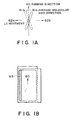
- Figures 1A and 1B are explanatory views for illustrating a cell thickness increase along a cell side in relation with liquid crystal movement directions.
- Figure 2 is an explanatory view for illustrating an alignment state occurring in a chiral smectic liquid crystal used in the invention.
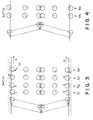
- Figures 3 and 4 are explanatory views for illustrating changes in director orientation according to various positions between substrates in C1 alignment and C2 alignment, respectively.
- Figures 5A and 5B are schematic sectional views of smectic layer structures utilized in the present invention.
- Figure 6 is an illustration of an X-ray diffraction method for analyzing the smectic layer structure.
- Figures 7A and 7B are diagrams showing X-ray diffraction patterns.
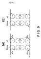
- Figure 8 is a schematic illustration showing C-director arrangements at various positions between the substrates in uniform alignment states.
- Figure 9 is a schematic illustration showing C-director arrangements at various positions between the substrates in the uniform alignment state utilized in the present invention.
- Figure 10 is a microscopic photograph (x250) showing an alignment of a ferroelectric liquid crystal obtained by gradual cooling from isotropic phase.
- Figure 11 is a microscopic photograph (x250) showing an alignment of a ferroelectric liquid crystal subjected to the treatment method according to the present invention.
- Figures 12A and 12B are X-ray diffraction diagrams showing a layer structure change.
- Figure 13 is a schematic sectional view of a liquid crystal device utilized in the present invention.
- Figures 14A - 14C are schematic sectional views showing various smectic layer structures.
- Figure 15 in a schematic sectional view of a smectic layer structure for illustrating alignment defects.
- Figure 16 is a schematic sectional view of an embodiment of the liquid crystal device according to the invention.
- Figure 17 is a graph showing a temperature-dependence of cone angle of a liquid crystal used in an Example of the present invention.
- Figure 18 is a schematic view for illustrating an alignment used in an Example of the present invention.
- Figure 19 is a waveform diagram showing a set of driving signal waveforms used in an Example of the present invention.
- the increase in cell thickness at a cell side is recognized to be caused by a pressure increase which in turn is caused by movement of liquid crystal molecules in a particular direction due to driving.
- a force causing the liquid crystal molecule movement may be attributable to an electrodynamic effect caused by perturbation of liquid crystal molecule dipole moments in an AC-like electric field caused by continuation of drive pulses.
- the directions 62a and 62b of the liquid crystal movement are determined in relation with the rubbing direction 60 and the average liquid crystal molecular axis position 61a or 61b as shown in Figure 1A.
- the moving direction of liquid crystal molecules is related with the rubbing direction, the above-mentioned phenomenon is assumed to depend on the pre-tilt state at the substrate surfaces.
- reference numeral 61a (or 61b in a reverse orientation state) denotes an average molecular axis (director) orientation.
- liquid crystal molecules (described herein as having a negative spontaneous polarization) are oriented to provide the average molecular axis 61a and are supplied with a certain strength of AC electric field not causing a switching to the orientation state 61b, the liquid crystal molecules are liable to move in the direction of an arrow 62a in the case where the substrates are provided with rubbing axes extending in parallel and in the same direction 60.
- the direction of the liquid crystal movement can be different depending on the liquid crystal material and the liquid crystal cell conditions.
- the liquid crystal movement occurs as shown in Figure 1A.
- the liquid crystal molecules in the entire cell are placed in a state providing an average molecular axis direction 61a, the liquid crystal molecules in the cell are liable to move under AC application in the direction of the arrow 62a, i.e., from the right to the left in the figure.
- the cell thickness in a region 63 is increased gradually to show a yellowish tint. If the liquid crystal molecules are placed in a state providing an average molecular axis 61b, the liquid crystal movement under AC application is caused in the reverse direction 62b.
- the liquid crystal movement is caused in a direction perpendicular to the rubbing direction, i.e., in the direction of extension of smectic layers. Accordingly, it is assumed that a state of the smectic layer structure is a factor of the liquid crystal movement.
- the liquid crystal movement adversely affects the durability as a display device of a liquid crystal device in a long term of continuous drive. Further, this liquid crystal movement phenomenon depends on an alignment state in the cell. More specifically, this phenomenon hardly occurs in C2 alignment but is remarkably observed in C1 alignment and uniform alignment described hereinafter.
- the two alignment states C1 and C2 may be explained by a difference in chevron structure of smectic layers as shown in Figure 2.
- reference numeral 41 denotes a smectic layer showing ferroelectricity
- 42 denotes a C1 alignment region
- 43 denotes a C2 alignment region.
- a smectic liquid crystal generally has a layer structure and causes a shrinkage of layer pitch when it is transformed from SmA (smectic A) phase into SmC (smectic C) phase or SmC* (chiral smectic C) phase, to result in a structure accompanied with a bending of layers between the upper and lower substrates 46a and 46b (chevron structure) as shown in Figure 2.
- the bending of the layers 41 can be caused in two ways corresponding to the C1 and C2 alignment as shown.
- liquid crystal molecules at the substrate surfaces are aligned to form a certain angle ⁇ or ⁇ C (pre-tilt) as a result of rubbing in a direction A in such a manner that their heads (leading ends) in the rubbing direction are up (or away) from the substrate surfaces 46a and 46b.
- pre-tilt the pre-tilt
- the C1 and C2 alignment states are not equivalent to each other with respect to their elastic energy, and a transition between these states can be caused at a certain temperature or when supplied with a mechanical stress.
- a boundary 44 of transition from C1 alignment (42) to C2 alignment (43) in the rubbing direction A looks like a zigzag lightning and is called a lightning defect
- a boundary 45 of transition from C2 alignment (43) to C1 alignment (42) forms a broad and moderate curve and is called a hairpin defect.
- FIG 3 is a schematic view illustrating director positions between the substrates in the respective states in C1 alignment. More specifically, at 51 - 54 are respectively shown changes in director positions between the substrates in the form of projections of directors onto cone bottoms as viewed from each bottom. At 51 and 52 is shown a splay state, and at 53 and 54 is shown a director arrangement which is believed to represent a uniform alignment state. As is understood from Figure 3, at 53 and 54 representing a uniform state, the molecule position (director) is different from that in the splay state either at the upper substrate or lower substrate.
- Arrows 57 represent the dipole moment ( ⁇ s) of liquid crystal molecules at the boundary, and an arrow A represents a rubbing direction.
- Figure 4 shows two states in C2 alignment between which no switching is observed at the boundaries but an internal switching is observed.
- the uniform state in C1 alignment provides a larger tilt angle ⁇ a and thus a higher brightness and a higher contrast than the conventionally used bistable state in C2 alignment.
- Figures 5A and 5B schematically show smectic layer structures of liquid crystal cells having a relatively small pretilt angle ⁇ C of about 2 degrees and subjected to parallel rubbing and anti-parallel rubbing, respectively.
- ⁇ C pretilt angle
- FIG. 6 is an illustration of the measurement system with an optical arrangement, including a cell 30 as an object of measurement to which incident X-rays having a wave number vector ki enter at an incident angle or cell rotation angle ⁇ and from which scattered X-rays having a wave number vector ks are issued at a Bragg angle 2 ⁇ B .
- the Bragg angle 2 ⁇ B may be obtained by measuring an angle corresponding to a scattering center of scattered X-rays detected by a detector while changing the position of the detector.
- Figure 7B shows a curve (E) as an example chart of X-ray diffraction intensity versus the rotation angle of a detector.
- a liquid crystal assumes a layer structure in its inherent bulk state in a random direction.
- a sharp peak is detected at an angle satisfying the Bragg condition, i.e., at a Bragg angle 2 ⁇ B .
- the peak provides a half-value width or full width at half maximum (FWHM) ⁇ 0 which is almost constant unless the factors affecting the accuracy of the measurement system, such as the slit width, are not changed and thus can be used as a reference of half-value width of diffraction peaks.
- the uniformity or homogeneity of a layer structure of a liquid crystal in the state of being confined in a cell can be evaluated in terms of a ratio of the half-value width of its diffraction peak to the reference value ⁇ 0 .
- a curve (A) in Figure 7A represents a result of measurement of diffraction intensity (arbitrary scale) versus cell rotation angle ⁇ with respect to a low-pretilt angle cell as described above.
- the measurement condition is the same as the curve (E) except that the detector position is fixed at 2 ⁇ B and the cell is rotated.
- cell A a specific example of such a low-pretilt angle cell (referred to as "cell A") will be described.
- a glass substrate provided with transparent electrodes was coated with tantalum oxide by sputtering and then coated with 1 % NMP (N-methylpyrrolidone)-solution of polyamide acid ("LP64", available from Toray K.K.), followed by baking at 270 o C for 1 hour and rubbing.
- NMP N-methylpyrrolidone
- This substrate and another substrate treated in the same manner were applied to each other to form a blank cell.
- the cell showed a pretilt angle of 2.5 degrees as measured by the crystal rotation method.
- the blank cell was then filled with a mixture ferroelectric liquid crystal containing a phenylpyrimidine as a principal constituent having a tilt angle of 15 degrees at room temperature, a layer inclination angle of 10 degrees at room temperature and showing the following phase transition series: Crystal -15 o C / SmC* 67 o C / SmA 89 o C / Ch. 96 o C / Iso.
- the liquid crystal cell did not satisfy the above-mentioned relationship (1) and provided C2 alignment as described above.
- the half-value width of X-ray diffraction peak was about 1.4 degrees as shown in the curve (A) in Figure 7A, which was about 28 times the above-mentioned reference value ⁇ 0 .
- the liquid crystal in the cell showed a considerable difference in order of layer structure from that in its bulk state.
- the diffraction peak given by the cell A showed the sharpest diffraction peak at a good reproducibility at least among a large number of cells measured by us, and substantially no alignment defect causing a disorder of layer structure was found.
- curves (B) - (D) represent X-ray diffraction peaks given by cells of an identical structure having an alignment film providing a high pretilt angle of, e.g., 10 degrees or higher.
- the half-value width of these diffraction peaks may be denoted by ⁇ h .
- a relationship between these half-value widths of X-ray diffraction peaks and the above-mentioned liquid crystal moving velocity will be described with reference to Examples and Comparative Examples appearing hereinafter.
- the dipole moment of a liquid crystal molecule at one substrate boundary is the same direction as at 51 and 52 but the dipole moment of a liquid crystal molecule at the other substrate boundary (upper boundary at 53 and lower boundary at 54) is directed from the liquid crystal layer toward the substrate. This direction may be called "outward".
- a conventional device generally has provided an alignment state wherein liquid crystal molecules giving outward and inward dipole moments provide different pretilt angles as shown in Figure 3.
- an alignment state giving different pretilt angles depending on dipole moment directions has been generally realized because the interaction between a substrate boundary and a liquid crystal molecule in the vicinity of the substrate boundary is different depending on the dipole moment direction of the liquid crystal molecule.
- pretilt angles are defined with respect to pretilt angles. That is, in SmC* phase, ⁇ 1 Ci and ⁇ 1 Co are used to denote pretilt angles given by liquid crystal molecules have inward and outward dipole moments, respectively, in the vicinity of an upper substrate. Similarly, symbols ⁇ 2 Ci and ⁇ 2 Co are used to denote pretilt angles given by liquid crystal molecules in the vicinity of a lower substrate.
- ⁇ 1 A and ⁇ 2 A are used to denote pretilt angles given by liquid crystal molecules in the vicinity of an upper substrate and a lower substrate, respectively, in SmA phase.
- each pretilt angle ⁇ C is represented by the length of a perpendicular line to an upper or lower substrate from an intersection of a C-director with a circle representing the projection of a cone.
- Figure 8(A) represents a case where an identical aligning treatment is applied to both an upper substrate 11 and a lower substrate 12.
- ⁇ 1 A ⁇ 2 A in SmA phase but, in SmC* phase, the pretilt angles are generally different between the upper and lower substrates due to a difference in direction of dipole moment ⁇ s.
- Figure 8(A) shows a case of ⁇ 1 A ⁇ ⁇ 2 A as developed by, e.g., by rubbing upper and lower substrates under different conditions.
- the pretilt angles are asymmetrical between the upper and lower substrates already in SmA phase, the pretilt angles are different not only corresponding to the difference between inward ⁇ s and outward ⁇ s but also corresponding to the difference between UP and DOWN of Ps in SmC* phase unlike a symmetry as observed in Figure 8(A).
- Figure 8(C) refers to a case of ⁇ 1 A > ⁇ 2 A opposite to the case of Figure 8(B).
- an alignment state satisfying the following relationship (2) can be realized if
- Figure 9(A) shows an example of alignment sate giving a symmetry of pretilt angle between upper and lower substrates.
- an AC application treatment is applied to a ferroelectric liquid crystal cell showing a pretilt angle of at least 10 degrees between a substrate boundary and a liquid crystal molecule in the vicinity of the substrate boundary.
- the cell (device) it is further preferred to subject the cell (device) to a temperature change, particularly a temperature increase and/or decrease within the smectic phase, so as to realize a homogeneous alignment capable of reducing the liquid crystal movement.
- Figure 11 shows that the wrinkle alignment defects shown in Figure 10 have been removed: 100 o C -4 o C/min / (40 o C 4 o C/min / AC ⁇ 7 V 100 Hz 75 o C -4 o C/min / AC ⁇ 7 V 100 Hz 40 o C) x three times
- ⁇ 1 ( ⁇ 2 ) denotes a first (second) diffraction peak angle
- ⁇ 1 ( ⁇ 2 ) denotes a layer inclination angle corresponding to the first (second) diffraction peak
- FWHM 1 (FWHM 2 ) denotes a half-value width or full width at half maximum of the first (second) diffraction peak.
- the increase in integrated intensity of a diffraction peak shows that a degree of order of layer structure has been increased. Further, a smaller half-value width of a peak shows that the layer structure has been converted into one with a clearer chevron structure.
- the liquid crystal cell includes a pair of an upper substrate 1311a and a lower substrate 1311b disposed in parallel with each other and provided with, e.g., about 400 - 3000 ⁇ -thick transparent electrodes 1312a and 1312b. Between the upper substrate 1311a and the lower substrate 1311b is disposed a ferroelectric liquid crystal 1315.
- the transparent electrodes 1312a and 1312b may be coated with, e.g., 10 to 3000 ⁇ -thick insulating films 1313a and 1313b.
- the insulating films may comprise an inorganic oxide of a coating-baking type or a sputtering film, or may comprise a laminate film of two or more layers.
- the alignment control films 1314a and 1314b are formed above the insulating films 1313a and 1313b in a thickness of ordinarily 50 - 1000 ⁇ .
- the alignment control films may ordinarily comprise a film of a polymer, preferably a film providing a high pretilt angle, such as that of a fluorine-containing polyimides, in the present invention.
- the pretilt angle may preferably be 10 - 30 degrees.
- Such polymer films may be rubbed as an aligning treatment.
- the ferroelectric liquid crystal 1315 may be in chiral smectic phase, inclusive of chiral smectic C phase (Sm*C), H phase (Sm*H), I phase (Sm*I), K phase (Sm*K) or G phase (Sm*G).
- a particularly preferred class of liquid crystals may be those showing cholesteric phase on a higher temperature side, including a pyrimidine-based mixture crystal showing the following phase transition series and physical properties.
- An FLC (ferroelectric liquid crystal) device was sandwiched between right-angle-cross nicol polarizers and rotated horizontally relative to the polarizers under application of a DC voltage of 10 - 30 volts between the upper and lower substrates to find a first extinction position (a position providing the lowest transmittance), and then a DC voltage of a polarity opposite to the above DC voltage is applied between the substrates to find a second extinction position.
- a cone angle H ⁇ was measured as a half of the angle between the first and second extinction positions.
- An FLC device sandwiched between right angle cross nicol polarizers was supplied with a single pulse of one polarity exceeding the threshold voltage of the ferroelectric liquid crystal and was then rotated under no electric field horizontally relative to the polarisers to find a first extinction position. Then, the FLC device was supplied with a single pulse of the opposite polarity exceeding the threshold voltage of the ferroelectric liquid crystal and was then rotated under no electric field relative to the polarizers to find a second extinction position.
- An apparent tilt angle ⁇ a was measured as a half of the angle between the first and second extinction positions.
- Smectic layer structures were analyzed by an X-ray diffraction method.
- the measurement method was basically similar to the one reported by Clark and Lagerwall (Japan Display '86, Sept. 30 - Oct. 2, 1986, pp. 456 - 458) or the one reported by Ohuchi et al (J.J.A.P., 27 (5) (1988) pp. 725 - 728).
- a liquid crystal layer spacing was measured by applying a sample liquid crystal on a glass plate, subjecting the sample liquid crystal to 2 ⁇ / ⁇ scanning similarly as in the ordinary powder X-ray diffraction and then applying the Bragg equation to the measured value.
- the layer structure of the sample liquid crystal in a cell structure is analyzed by fixing the X-ray detector at a diffraction angle 2 ⁇ corresponding to the measured layer spacing and subjecting the sample cell to ⁇ -scanning as reported in the above-mentioned method.
- a sample liquid crystal cell may for example be prepared by providing a 80 ⁇ m-thick glass plate, coating the glass plate sequentially with a 400 to 3000 ⁇ -thick (e.g., 1500 ⁇ -thick) indium-tin-oxide film, a 100 to 3000 ⁇ -thick (e.g., 900 ⁇ -thick) insulating film and a 50 to 1000 ⁇ -thick (e.g., 200 ⁇ -thick) alignment control film of the same polymer and rubbing the alignment control film, applying the thus treated glass plate and another glass plate treated identically to each other to form a cell so as to provide a pretilt angle of, e.g., at least 10 degrees, and filling the cell with the sample ferroelectric liquid crystal in a liquid crystal layer thickness of 1.5 ⁇ m.
- a 400 to 3000 ⁇ -thick e.g., 1500 ⁇ -thick
- a 100 to 3000 ⁇ -thick e.g., 900 ⁇ -th
- a rotating anticathode-type X-ray diffraction apparatus e.g., "MXP-18", available from MAC Science Co.
- the X-ray diffraction conditions included the following:
- a pair of substrates rubbed in mutually parallel and opposite directions were applied to each other to form a cell having a cell gap of 20 ⁇ m, which was then filled with a liquid crystal mixture (A) assuming SmA phase in the temperature range of 0 - 60 o C.
- the liquid crystal cell was rotated in a plane perpendicular to the pair of substrates and including the aligning treatment axis and, during the rotation, the cell was illuminated with a helium-neon laser beam having a polarization plane forming an angle of 45 degrees with respect to the rotation plane in a direction normal to the rotation plane, whereby the intensity of the transmitted light was measured by a photodiode from the opposite side through a polarizer having a transmission axis parallel to the polarization plane.
- a glass substrate provided with transparent electrodes was coated with a tantalum oxide film by sputtering and then coated with 1 % NMP-solution of polyamide acid ("LQ1802", available from Hitachi Kasei K.K.), followed by baking at 270 o C for 1 hour and rubbing.
- This substrate and another substrate treated in the same manner were applied to each other with a cell gap of 1.5 ⁇ m so that their rubbing directions were almost identical but formed a right-screw intersection angle of about 10 degrees between the upper and lower substrates.
- the cell showed a pretilt angle of 17 degrees according to the crystal rotation method.
- the cell was then filled with the same mixture liquid crystal as used in the above-mentioned cell A, and the resultant cell was gradually cooled from isotropic phase at a rate of -4 o C/min. Then, the cell was subjected to three cycles of a realigning treatment of heating to SmA phase (75 o C) followed by re-cooling to SmC* phase (40 o C), respectively at a rate of 4 o C while applying alternating rectangular waveforms of 100 Hz and ⁇ 10 volts to obtain a desired alignment state.
- the resultant cell is referred to as cell B.
- the cell showed an apparent tilt angle ⁇ a of about 11 degrees, thus satisfying the above-mentioned relationships (1) and (2) and showing homogeneous C1 uniform alignment.
- the curve (B) in Figure 7A represents an X-ray diffraction pattern of the cell B, thus showing a sharp diffraction peak comparable with that of the cell A and a half-value width ⁇ h of about 1.9 degrees. Further, as a result of alignment observation through a polarizing microscope, substantially no alignment defects due to disorder of layer structure were detected. Accordingly, similarly as the cell A, a homogeneous layer structure retaining a substantially constant layer spacing as shown in Figure 5A was confirmed.
- a liquid crystal display device (cell) having a sectional structure as shown in Figure 13 may be formed similarly as in the above Example.
- the liquid crystal cell include substrates (glass plates) 1311a and 1311b provided with transparent electrodes 1312a and 1312b of, e.g., In 2 O 3 or ITO (indium tin oxide), which are further coated with 200 to 3000 ⁇ -thick insulating films 1313a and 1313b of, e.g., SiO 2 , TiO 2 and Ta 2 O 5 , and 50 to 1000 ⁇ -thick alignment control films 1314a and 1314b of a polyimide providing a high pretilt angle as described above.
- the alignment control films 1314a and 1314b have been rubbed in directions which are identical but intersect each other at a mutually right-screw angle of 3 - 20 degrees.
- a ferroelectric smectic liquid crystal 1315 in a thickness which is sufficiently small (e.g., 0.1 - 3 ⁇ m) to suppress the formation of a helical structure of the ferroelectric liquid crystal and place the ferroelectric liquid crystal 1315 in a bistable alignment state.
- the liquid crystal layer thickness is held by spacer beads 1316 of, e.g., silica oralumina.
- the entire cell structure is held between a pair of polarizers 1317a and 1317b to provide a panel having a display area of 114 mm x 228 mm.
- a panel thus prepared was subjected to the above-mentioned realigning treatment and the alignment in the cell was brought to one providing an average molecular axis direction 61 shown in Figure 1A. Then, the panel was subjected to continual application of rectangular pulses of a pulse width of 24 ⁇ s, a voltage amplitude of 40 volts and a duty ratio of 1/2 for about 7 hours. As a result of measurement of the cell thickness increase at the region 63 in Figure 18, the increase was only about 5 % with respect to the initial value.
- a cell of the same structure as the cell B was, after being gradually cooled from isotropic phase, subjected to several cycles of a realigning treatment of heating into SmA phase followed by re-cooling to Sm*C phase in the same manner as in Example 1 to obtain a cell C.
- the cell C provided an X-ray diffraction pattern (C) in Figure 7A.
- a cell of the same structure as the cell B was gradually cooled from isotropic phase to provide a cell D without a realigning treatment.
- the broadness of the diffraction peak means that the order of smectic layer structure is lowered in some way. This may be attributable to a phenomenon that the liquid crystal in the state of being gradually cooled from isotropic phase is strongly affected by the substrate boundaries to cause a curving of the smectic layers as shown in Figures 14A and 14B, but detailed mechanisms have not yet been clarified.
- alignment defects attributable to disorder in layer structure were detected.
- Such alignment defects might be attributable to a phenomenon that the curving or bending of layers so as to keep the layer spacing to be locally constant caused disalignments or alignment defects as denoted by reference numeral 50 in Figure 15, but details have not been clarified as yet.
- FIG 16 is a sectional view showing another suitable embodiment according to the present invention.
- the liquid crystal cell includes a pair of an upper substrate 31a and a lower substrate 31b disposed in parallel with each other and provided with about 400 to 2000 ⁇ -thick transparent electrodes 32a and 32b.
- a ferroelectric liquid crystal 35 Between the upper substrate 31a and the lower substrate 31b is disposed a ferroelectric liquid crystal 35, preferably a ferroelectric smectic liquid crystal placed in a non-helical structure providing at least two stable states.
- the transparent electrodes 32a and 32b are covered with alignment control films 34a and 34b of, e.g., 10 to 1000 ⁇ -thick films of a polymer, such as a polyimide.
- the alignment control films 34a and 34b have been rubbed in directions which are parallel and identical to each other. It is also possible to have the rubbing directions intersect each other at an angle of 5 - 20 degrees. It is also possible to insert, e.g., 200 to 3000 ⁇ -thick insulating films 33a and/or 33b of, e.g., SiO 2 , TiO 2 or Ta 2 O 5 , between the alignment control films 34a, 34b and the transparent electrodes 32a, 32b.
- the spacing between the substrates is held by, e.g., silica beads of, e.g., about 1.5 ⁇ m (generally, 0.1 - 3.5 ⁇ m) in average diameter, dispersed within the liquid crystal layer 35.
- the upper substrate 31a and the lower substrate 31b have been subjected to an equivalent aligning treatment so as to develop effectively equal pretilt angles.
- the ferroelectric liquid crystal 35 may be in chiral smectic phase, more specifically chiral smectic C phase (Sm*C), H phase (Sm*H) or I phase (Sm*I).
- a particularly preferred class of liquid crystals may be those showing cholesteric phase on a higher temperature side, including a pyrimidine-based mixture crystal showing the following phase transition series and physical properties.
- a liquid crystal cell prepared in the above-described manner by using the pyrimidine-based mixture liquid crystal was gradually cooled from isotropic phase, and then subjected to a re-aligning treatment including re-heating into SmA phase and then re-cooling into Sm*C phase under application of alternating rectangular waves of 100 Hz and ⁇ 10 volts in the same manner as in Example 1 to obtain a desired alignment state.
- pretilt angles were measured according to the TIR (total inner reflection) method described in, e.g., Appl. Phys. Lett. Vol. 53, No. 24, 2397 (1989).
- the measured cell had a structure comprising a hemispherical prism of a high refractive index in place of the upper substrate 31a in the cell shown in Figure 16, to measure a pretilt angle ⁇ A in SmA phase and pretilt angles ⁇ Ci and ⁇ Co in Sm*C phase for inward and outward dipole moments, respectively, of liquid crystal molecules in the vicinity of a liquid crystal boundary contacting the hemispherical prism.
- the alignment in a liquid crystal cell prepared in the above-described manner was entirely brought to an orientation providing an average molecular axis direction 61 and subjected to continual application of rectangular pulses of a pulse width of a voltage amplitude of 40 volts and a duty of 1/2 for about 7 hours.
- the cell thickness increase was only about 5 % with respect to the initial value.
- the bistability was also very good.
- a cell of the same structure as in Example 3 was prepared and gradually cooled from isotropic phase, followed by no realigning treatment.
- Example 3 The above cell was subjected to continual voltage application in the same manner as in Example 3, whereby the cell thickness increase amounted to about 30 % with respect to the initial value.
- a glass substrate measuring 7.5 cm x 7.5 cm and provided with transparent electrodes was coated with a tantalum oxide film by sputtering and then coated with 1 % NMP-solution of a fluorine-containing polyimide precursor, followed by baking at 270 o C for 1 hour and rubbing.
- This substrate and another substrate treated in the same manner were applied to each other with a cell gap of 1.5 ⁇ m therebetween to form a cell, so that their rubbing directions were almost identical but formed an intersection angle of a right-screw or clockwise screw (as viewed from above the cell) of 10 degrees.
- the cell showed a pretilt angle of 20 degrees according to the crystal rotation method.
- the cell was filled with a phenylpyrimidine-based mixture liquid crystal showing a cone angle of 14 degrees at room temperature, a layer inclination angle of 12 degrees. and the following phase transition series: Cryst. -20 o C / Sm*C 67 o C / SmA 85 o C / Ch. 91 o C / Iso.
- Figure 17 shows the temperature-dependence of the cone angle H ⁇ of the liquid crystal by using a temperature scale normalized with the AC phase-transition temperature (67 o C) of the liquid crystal.
- the liquid crystal cell was aged for 5 hours at 100 o C and then subjected to the following series of cooling - realigning treatment: 100 o C -4 o C/min / (40 o C 4 o C/min / AC ⁇ 7 V 100 Hz 75 o C -4 o C/min / AC ⁇ 7 V 100 Hz 40 o C) x three times C1 alignment was retained and electric field switching between uniform states was possible over the entire temperature range of Sm*C. Experiments were thereafter carried out at 30 o C. The apparent tilt angle ⁇ a under the condition was 11.5 degrees.
- the cell was sandwiched with cross nicol polarizers to observe the coloring with naked eyes, whereby no region of cell thickness increase was recognized by coloring.
- a liquid crystal cell prepared in the same manner as in Example 4 up to the aging at 100 o C was then subjected to cooling at a rate of -4 o C/min to 50 o C, and 10 min. of AC application at 50 o C of AC ⁇ 7 volts and 100 Hz.
- the cell was sandwiched with cross nicol polarizers to observe the coloring with naked eyes, whereby no region of cell thickness increase was recognized by coloring.
- a liquid crystal cell prepared in the same manner as in Example 4 up to the aging at 100 o C was then subjected to cooling at a rate of -4 o C/min to 25 o C, and 10 min. of AC application at 25 o C of AC ⁇ 7 volts and 100 Hz.
- the cell was sandwiched with cross nicol polarizers to observe the coloring with naked eyes, whereby no region of cell thickness increase was recognized by coloring.
- a liquid crystal cell prepared in the same manner as in Example 4 up to the aging at 100 o C was then subjected to the following treatment: 100 o C -4 o C/min / 75 o C -1 o C/min / AC ⁇ 7 V 100 Hz 30 o C
- the cell was sandwiched with cross nicol polarizers to observe the coloring with naked eyes, whereby no region of cell thickness increase was recognized by coloring.
- Example 8 X-ray diffraction analysis was performed similarly as in Example 4.
- the results of measurement of the layer inclination angle ⁇ , peak half-value width (FWMH) and diffraction peak area are summarized in Table 8 appearing hereinafter. As shown in Table 8.
- the peak area and the half-value width obtained in this Example 7 were respectively 83 % and 1.18 times of those of Comparative Example 5 described hereinafter.
- a liquid crystal cell prepared in the same manner as in Example 4 up to the aging at 100 o C was then subjected to the following treatment: 100 o C -4 o C/min / (30 o C 4 o C/min / 75 o C -4 o C/min / 30 o C) x 3 times
- the cell was sandwiched with cross nicol polarizers to observe the coloring with naked eyes, whereby no region of cell thickness increase was recognized by coloring.
- Example 8 X-ray diffraction analysis was performed similarly as in Example 4.
- the results of measurement of the layer inclination angle ⁇ , peak half-value width (FWMH) and diffraction peak area are summarized in Table 8 appearing hereinafter. As shown in Table 8.
- the peak area and the half-value width obtained in this Example 8 were respectively 80 % and 1.23 times of those of Comparative Example 5 described hereinafter.
- a liquid crystal cell prepared in the same manner as in Example 4 up to the aging at 100 o C was then cooled at a rate of -4 o C/min to 30 o C.
- the cell was then subjected to evaluation in the same manner as in Example 4 without further treatment.
- C1 alignment was retained and switching by electric field between uniform states was possible.
- the apparent tilt angle ⁇ a was 11.5 degrees.
- the cell was sandwiched with cross nicol polarizers to observe the coloring with naked eyes, whereby the regions 83 and 85 were colored in yellow due to a remarkable thickness change in the case of displaying white.
- the pretilt angle was measured to be 9 degrees under the above-mentioned rubbing condition.
- C2 alignment appears in Sm*C phase at temperatures below 55 o C, whereby switching between homogeneous uniform states failed.
- a glass substrate measuring 7.5 cm x 7.5 cm and provided with transparent electrodes was coated with a tantalum oxide film by sputtering and then coated with 1 % NMP-solution of a polyamide acid as a precursor to a polyimide of the following structural formula: followed by baking at 270 o C for 1 hour and rubbing.
- This substrate and another substrate treated in the same manner were applied to each other with a cell gap of 1.5 ⁇ m therebetween to form a cell, so that their rubbing directions were almost identical but formed an intersection angle of a right-screw or clockwise screw (as viewed from above the cell) of 10 degrees.
- the cell showed a pretilt angle of 1.5 degrees according to the crystal rotation method.
- the cell was filled with the same phenylpyrimidine-based mixture liquid crystal as used in Example 4. The resultant liquid crystal showed homogeneous C2 splay alignment in Sm*C phase at temperatures below 63 o C.
- Example 4 X-ray diffraction analysis was performed similarly as in Example 4. The results of measurement of the layer inclination angle ⁇ , peak half-value width (FWMH) and diffraction peak area are summarized in Table 8 together with the results in Examples 4, 7, 8 and Comparative Example 3.
- the order of smectic layer structure can be increased even in a high pretilt angle cell with a pretilt angle of, e.g., at least 10 degrees, by applying the above-mentioned realigning treatment, whereby it has become possible to remarkably decrease the cell thickness change due to liquid crystal movement.
- a ferroelectric liquid crystal device wherein pretilt angles are corrected to provide an improved bistability and a high contrast alignment and also to remarkably decrease the local cell thickness change during drive.
- a ferroelectric liquid crystal device is constituted by disposing a ferroelectric liquid crystal between a pair of substrates having thereon electrodes for voltage application and provided with uniaxial alignment axes, as by rubbing, so as to provide a high pretilt angle of at least 10 degrees.
- a problematic liquid crystal movement in such a high-pretilt angle ferroelectric liquid crystal device is suppressed by improving a smectic layer structure therein, inclusive of a symmetry of pretilt angles at the pair of substrate boundary surfaces.
- Such an improved smectic layer structure is accomplished by a realigning treatment after cooling to the chiral smectic phase or in the final stage of the cooling to the chiral smectic phase as by application of an AC electric field and/or by repetitive heating-cooling in the chiral smectic phase.
- the improved smectic layer structure is represented by, e.g., an X-ray diffraction peak having an increased peak area and/or a decreased half-value width.
Landscapes
- Physics & Mathematics (AREA)
- Chemical & Material Sciences (AREA)
- Crystallography & Structural Chemistry (AREA)
- Nonlinear Science (AREA)
- General Physics & Mathematics (AREA)
- Optics & Photonics (AREA)
- Liquid Crystal (AREA)
- Inorganic Insulating Materials (AREA)
Applications Claiming Priority (5)
| Application Number | Priority Date | Filing Date | Title |
|---|---|---|---|
| JP3281692A JPH05203959A (ja) | 1992-01-24 | 1992-01-24 | 強誘電性液晶素子 |
| JP32816/92 | 1992-01-24 | ||
| JP4021192 | 1992-01-30 | ||
| JP40211/92 | 1992-01-30 | ||
| EP93100950A EP0553727B1 (de) | 1992-01-24 | 1993-01-22 | Verfahren zur Behandlung einer chiralen smektischen Flüssigkristallvorrichtung |
Related Parent Applications (1)
| Application Number | Title | Priority Date | Filing Date |
|---|---|---|---|
| EP93100950A Division EP0553727B1 (de) | 1992-01-24 | 1993-01-22 | Verfahren zur Behandlung einer chiralen smektischen Flüssigkristallvorrichtung |
Publications (1)
| Publication Number | Publication Date |
|---|---|
| EP0844510A1 true EP0844510A1 (de) | 1998-05-27 |
Family
ID=26371402
Family Applications (2)
| Application Number | Title | Priority Date | Filing Date |
|---|---|---|---|
| EP98100899A Withdrawn EP0844510A1 (de) | 1992-01-24 | 1993-01-22 | Ferroelektrische Flüssigkristallvorrichtung und Verfahren zur Behandlung derselben |
| EP93100950A Expired - Lifetime EP0553727B1 (de) | 1992-01-24 | 1993-01-22 | Verfahren zur Behandlung einer chiralen smektischen Flüssigkristallvorrichtung |
Family Applications After (1)
| Application Number | Title | Priority Date | Filing Date |
|---|---|---|---|
| EP93100950A Expired - Lifetime EP0553727B1 (de) | 1992-01-24 | 1993-01-22 | Verfahren zur Behandlung einer chiralen smektischen Flüssigkristallvorrichtung |
Country Status (4)
| Country | Link |
|---|---|
| US (2) | US5790223A (de) |
| EP (2) | EP0844510A1 (de) |
| AT (1) | ATE169414T1 (de) |
| DE (1) | DE69320073T2 (de) |
Families Citing this family (24)
| Publication number | Priority date | Publication date | Assignee | Title |
|---|---|---|---|---|
| US5781266A (en) * | 1993-09-27 | 1998-07-14 | Matsushita Electric Industrial Co., Ltd. | Ferroelectric liquid crystal display device and method for producing the same |
| JP2942161B2 (ja) * | 1993-12-28 | 1999-08-30 | キヤノン株式会社 | 液晶の配向処理方法、該方法を用いた液晶素子の製造方法、並びに液晶素子 |
| US5815230A (en) * | 1994-01-27 | 1998-09-29 | Canon Kabushiki Kaisha | Liquid crystal device and process for production thereof |
| US5798056A (en) * | 1995-02-01 | 1998-08-25 | Canon Kabushiki Kaisha | Aligning method of liquid crystal, production process of liquid crystal device, and liquid crystal device |
| DE69625889D1 (de) * | 1995-07-03 | 2003-02-27 | Citizen Watch Co Ltd | Flüssigkristallvorrichtung |
| US5932136A (en) * | 1995-10-20 | 1999-08-03 | Canon Kabushiki Kaisha | Liquid crystal device and liquid crystal apparatus |
| US5885482A (en) * | 1995-12-28 | 1999-03-23 | Canon Kabushiki Kaisha | Liquid crystal device, production process thereof and liquid crystal apparatus |
| GB9604461D0 (en) * | 1996-03-01 | 1996-05-01 | Secr Defence | Alignment of ferroelectric liquid crystal displays |
| JPH09311354A (ja) * | 1996-05-17 | 1997-12-02 | Sharp Corp | 液晶表示素子の製造方法 |
| US6020947A (en) * | 1996-11-06 | 2000-02-01 | Sharp Kabushiki Kaisha | Liquid crystal devices |
| JPH11100577A (ja) * | 1997-07-31 | 1999-04-13 | Canon Inc | 液晶の配向方法、液晶素子の製造方法、該製造方法により得られる液晶素子、液晶装置 |
| US6195147B1 (en) | 1997-08-01 | 2001-02-27 | Canon Kabushiki Kaisha | Liquid crystal substrate with optical modulation region having different alignment control forces |
| US6139927A (en) * | 1997-09-18 | 2000-10-31 | Canon Kabushiki Kaisha | Liquid crystal device |
| EP0967510A4 (de) * | 1997-12-05 | 2005-11-02 | Citizen Watch Co Ltd | Verfahren zur unterdrückung und beseitigung der bildträgheit von ferroelektrischen flüssigkristallgeräten |
| JP3559719B2 (ja) | 1998-01-13 | 2004-09-02 | キヤノン株式会社 | プラズマアドレス型の液晶表示装置 |
| JP3342430B2 (ja) | 1998-02-27 | 2002-11-11 | キヤノン株式会社 | 液晶素子及び液晶表示装置 |
| DE19825487A1 (de) * | 1998-06-08 | 1999-12-09 | Aventis Res & Tech Gmbh & Co | Monostabiles ferroelektrisches Akivmatrix-Display |
| JP2000199889A (ja) | 1999-01-06 | 2000-07-18 | Canon Inc | 液晶装置 |
| JP3667215B2 (ja) * | 1999-08-31 | 2005-07-06 | キヤノン株式会社 | 単結晶性薄膜およびその製造方法 |
| JP2002201473A (ja) | 2000-10-25 | 2002-07-19 | Canon Inc | スメクチック高分子液晶及びその製造方法、これを用いた液晶素子 |
| JP4712585B2 (ja) * | 2006-03-22 | 2011-06-29 | 本田技研工業株式会社 | 電動機の制御装置 |
| JP4754379B2 (ja) * | 2006-03-22 | 2011-08-24 | 本田技研工業株式会社 | 電動機の制御装置 |
| CN104298005B (zh) * | 2014-10-11 | 2017-02-22 | 深圳市华星光电技术有限公司 | 一种液晶显示面板的制作方法 |
| KR102712151B1 (ko) * | 2021-06-04 | 2024-10-02 | 삼성전자주식회사 | 강유전체 박막을 포함하는 3차원 반도체 메모리 장치 및 이의 제조 방법 |
Citations (1)
| Publication number | Priority date | Publication date | Assignee | Title |
|---|---|---|---|---|
| EP0444705A2 (de) * | 1990-03-02 | 1991-09-04 | Canon Kabushiki Kaisha | Flüssigkristallelement und Flüssigkristallvorrichtung, die dieses Element verwendet |
Family Cites Families (31)
| Publication number | Priority date | Publication date | Assignee | Title |
|---|---|---|---|---|
| US4958916A (en) * | 1980-01-08 | 1990-09-25 | Clark Noel A | Surface stabilized ferroelectric liquid crystal devices |
| US4367924A (en) * | 1980-01-08 | 1983-01-11 | Clark Noel A | Chiral smectic C or H liquid crystal electro-optical device |
| JPS61147232A (ja) * | 1984-12-20 | 1986-07-04 | Canon Inc | 液晶素子 |
| US4898456A (en) * | 1985-04-23 | 1990-02-06 | Canon Kabushiki Kaisha | Liquid crystal optical device |
| US4941736A (en) * | 1985-04-23 | 1990-07-17 | Canon Kabushiki Kaisha | Ferroelectric liquid crystal device and driving method therefor |
| GB2178581B (en) * | 1985-07-12 | 1989-07-19 | Canon Kk | Liquid crystal apparatus and driving method therefor |
| US4778259A (en) * | 1985-07-17 | 1988-10-18 | Canon Kabushiki Kaisha | Ferroelectric liquid crystal devices having reverse twist angle and stable states resulting from A.C. excitation |
| DE3630012A1 (de) * | 1985-09-04 | 1987-04-23 | Canon Kk | Ferroelektrische fluessigkristallvorrichtung |
| JPH0685032B2 (ja) * | 1985-10-17 | 1994-10-26 | キヤノン株式会社 | カイラルスメクティック液晶素子 |
| US4820026A (en) * | 1986-03-20 | 1989-04-11 | Canon Kabushiki Kaisha | Ferroelectric liquid crystal device with modified polyvinyl alcohol alignment film |
| GB8608116D0 (en) * | 1986-04-03 | 1986-05-08 | Secr Defence | Liquid crystal devices |
| US4796979A (en) * | 1986-04-07 | 1989-01-10 | Canon Kabushiki Kaisha | Ferroelectric liquid crystal device having dual laminated alignment films |
| JPS62278540A (ja) * | 1986-05-27 | 1987-12-03 | Canon Inc | 液晶素子、その配向制御法及びその駆動法 |
| JPS62284334A (ja) * | 1986-06-03 | 1987-12-10 | Canon Inc | 液晶装置 |
| GB8614838D0 (en) * | 1986-06-18 | 1986-07-23 | Gen Electric Co Plc | Liquid crystal devices |
| JP2667816B2 (ja) * | 1986-09-20 | 1997-10-27 | キヤノン株式会社 | 液晶素子 |
| US5164852A (en) * | 1986-12-16 | 1992-11-17 | Semiconductor Energy Laboratory Co., Ltd. | Method of orientating a ferroelectric liquid crystal layer by AC electric field |
| US5182549A (en) * | 1987-03-05 | 1993-01-26 | Canon Kabushiki Kaisha | Liquid crystal apparatus |
| US4900132A (en) * | 1987-04-13 | 1990-02-13 | Tektronix, Inc. | Chiral liquid crystal cell |
| FR2618587B1 (fr) * | 1987-07-20 | 1992-04-24 | Commissariat Energie Atomique | Ecran a cristal liquide, a electrodes opacifiees dans la zone non commutable de l'ecran et procedes d'obtention d'espaceurs et de traitement de cet ecran |
| US4932758A (en) * | 1987-09-17 | 1990-06-12 | Canon Kabushiki Kaisha | Ferroelectric smectic liquid crystal device having a bistable alignment state providing two stable orientation states |
| US4973138A (en) * | 1987-10-27 | 1990-11-27 | Semiconductor Energy Laboratory Co., Ltd. | Liquid crystal device and manufacturing method for the same |
| JP2651204B2 (ja) * | 1988-07-14 | 1997-09-10 | キヤノン株式会社 | 液晶装置の駆動法 |
| JP2623137B2 (ja) * | 1989-03-07 | 1997-06-25 | キヤノン株式会社 | カイラルスメクチック液晶素子ユニットおよびカイラルスメクチック液晶パネルの支持方法 |
| NL8901481A (nl) * | 1989-06-12 | 1991-01-02 | Philips Nv | Passieve ferro-elektrisch vloeibaar kristal weergeefinrichting en werkwijze ter vervaardiging daarvan. |
| GB9002105D0 (en) * | 1990-01-31 | 1990-03-28 | Stc Plc | Ferro electric liquid crystal cells |
| JPH04212127A (ja) * | 1990-04-03 | 1992-08-03 | Canon Inc | 液晶素子および表示装置 |
| JPH0799420B2 (ja) * | 1990-07-13 | 1995-10-25 | アルプス電気株式会社 | 強誘電性液晶素子 |
| JP2802685B2 (ja) * | 1991-01-08 | 1998-09-24 | キヤノン株式会社 | 強誘電性液晶装置 |
| JP2737032B2 (ja) * | 1991-03-28 | 1998-04-08 | キヤノン株式会社 | 液晶セル |
| JPH05158041A (ja) * | 1991-12-05 | 1993-06-25 | Canon Inc | 強誘電性液晶素子 |
-
1993
- 1993-01-22 AT AT93100950T patent/ATE169414T1/de not_active IP Right Cessation
- 1993-01-22 EP EP98100899A patent/EP0844510A1/de not_active Withdrawn
- 1993-01-22 DE DE69320073T patent/DE69320073T2/de not_active Expired - Fee Related
- 1993-01-22 EP EP93100950A patent/EP0553727B1/de not_active Expired - Lifetime
-
1995
- 1995-11-02 US US08/552,276 patent/US5790223A/en not_active Expired - Fee Related
- 1995-11-06 US US08/554,031 patent/US5543943A/en not_active Expired - Fee Related
Patent Citations (1)
| Publication number | Priority date | Publication date | Assignee | Title |
|---|---|---|---|---|
| EP0444705A2 (de) * | 1990-03-02 | 1991-09-04 | Canon Kabushiki Kaisha | Flüssigkristallelement und Flüssigkristallvorrichtung, die dieses Element verwendet |
Non-Patent Citations (2)
| Title |
|---|
| KODEN M ET AL: "The states of surface-stabilized ferroelectric liquid crystal with high-pretilt aligning film", JAPANESE JOURNAL OF APPLIED PHYSICS, PART 2 (LETTERS), 15 OCT. 1991, JAPAN, vol. 30, no. 10B, ISSN 0021-4922, pages L1823 - L1825, XP000235835 * |
| ORIHARA H ET AL: "Effect of a polyimide coat on the layer structure in a surface-stabilized ferroelectric liquid crystal cell", JAPANESE JOURNAL OF APPLIED PHYSICS, PART 2 (LETTERS), APRIL 1989, JAPAN, vol. 28, no. 4, ISSN 0021-4922, pages L676 - L678, XP000363644 * |
Also Published As
| Publication number | Publication date |
|---|---|
| EP0553727A2 (de) | 1993-08-04 |
| EP0553727B1 (de) | 1998-08-05 |
| ATE169414T1 (de) | 1998-08-15 |
| DE69320073D1 (de) | 1998-09-10 |
| DE69320073T2 (de) | 1999-02-25 |
| EP0553727A3 (en) | 1993-11-03 |
| US5790223A (en) | 1998-08-04 |
| US5543943A (en) | 1996-08-06 |
Similar Documents
| Publication | Publication Date | Title |
|---|---|---|
| EP0553727B1 (de) | Verfahren zur Behandlung einer chiralen smektischen Flüssigkristallvorrichtung | |
| EP0550846B1 (de) | Ferroelektrische Flüssigkristall-Anzeigevorrichtung und Verfahren zu ihrer Herstellung | |
| KR940005123B1 (ko) | 액정소자 및 액정소자를 사용한 액정장치 | |
| US5742369A (en) | Method of aligning liquid crystals by applying an alternating electric field under periodically changing temperature | |
| EP0831358A2 (de) | Flüssigkristallvorrichtungen mit einer Vielzahl von Domänen mit unterschiedlichen Schwellenspannungen zum Schalten von Flüssigkristallen | |
| US5172257A (en) | Twisted ferroelectric liquid crystal modulator for providing gray scale | |
| EP0539992B1 (de) | Flüssigkristall-Anzeigevorrichtung | |
| JP2612503B2 (ja) | 液晶素子 | |
| EP0496628B1 (de) | Ferroelektrische Flüssigkristall-Anzeigevorrichtung | |
| GB2174820A (en) | Ferroelectric smectic liquid-crystal device | |
| EP0637622B1 (de) | Flüssigkristallvorrichtung | |
| US5353141A (en) | Method for aligning treatment of liquid crystal device including varying with time the feeding speed of the rubbing roller | |
| EP0539991B1 (de) | Flüssigkristallvorrichtung und Anzeigevorrichtung | |
| KR0159969B1 (ko) | 액정 소자 및 이를 구동시키기 위한 액정 장치 | |
| EP0704744A1 (de) | Ferroelektrische Flüssigkristallvorrichtung | |
| US5557435A (en) | Liquid crystal device and display apparatus | |
| EP0532210B1 (de) | Flüssigkristallanzeige | |
| JP3083016B2 (ja) | 液晶の配向処理方法、及び液晶素子の製造方法 | |
| CA1304485C (en) | Liquid crystal display element and method for driving same | |
| JP3000504B2 (ja) | 液晶素子 | |
| JP3180171B2 (ja) | 強誘電性液晶素子 | |
| JP2663082B2 (ja) | 液晶素子 | |
| JPH05323255A (ja) | 液晶組成物およびこれを用いる液晶素子 | |
| JPH06186569A (ja) | 強誘電性液晶素子 | |
| JPH0553117A (ja) | 液晶素子 |
Legal Events
| Date | Code | Title | Description |
|---|---|---|---|
| PUAI | Public reference made under article 153(3) epc to a published international application that has entered the european phase |
Free format text: ORIGINAL CODE: 0009012 |
|
| AC | Divisional application: reference to earlier application |
Ref document number: 553727 Country of ref document: EP |
|
| AK | Designated contracting states |
Kind code of ref document: A1 Designated state(s): AT BE CH DE DK ES FR GB GR IT LI LU NL PT SE |
|
| 17P | Request for examination filed |
Effective date: 19981013 |
|
| 17Q | First examination report despatched |
Effective date: 20070801 |
|
| STAA | Information on the status of an ep patent application or granted ep patent |
Free format text: STATUS: THE APPLICATION HAS BEEN WITHDRAWN |
|
| 18W | Application withdrawn |
Effective date: 20080201 |