EP0844786A1 - Circuit pour la correction en S de la déflection horizontale avec capacité variable - Google Patents
Circuit pour la correction en S de la déflection horizontale avec capacité variable Download PDFInfo
- Publication number
- EP0844786A1 EP0844786A1 EP97402809A EP97402809A EP0844786A1 EP 0844786 A1 EP0844786 A1 EP 0844786A1 EP 97402809 A EP97402809 A EP 97402809A EP 97402809 A EP97402809 A EP 97402809A EP 0844786 A1 EP0844786 A1 EP 0844786A1
- Authority
- EP
- European Patent Office
- Prior art keywords
- correction
- horizontal
- condenser
- circuit
- signal
- Prior art date
- Legal status (The legal status is an assumption and is not a legal conclusion. Google has not performed a legal analysis and makes no representation as to the accuracy of the status listed.)
- Granted
Links
- 230000000694 effects Effects 0.000 abstract description 6
- 238000010586 diagram Methods 0.000 description 8
- 230000003247 decreasing effect Effects 0.000 description 6
- 230000010355 oscillation Effects 0.000 description 5
- 238000010276 construction Methods 0.000 description 2
- 238000007493 shaping process Methods 0.000 description 2
- 238000004804 winding Methods 0.000 description 2
- 230000006978 adaptation Effects 0.000 description 1
- 238000007792 addition Methods 0.000 description 1
- 238000007599 discharging Methods 0.000 description 1
- 230000005669 field effect Effects 0.000 description 1
- 238000012986 modification Methods 0.000 description 1
- 230000004048 modification Effects 0.000 description 1
- 238000006467 substitution reaction Methods 0.000 description 1
Images



Classifications
-
- H—ELECTRICITY
- H04—ELECTRIC COMMUNICATION TECHNIQUE
- H04N—PICTORIAL COMMUNICATION, e.g. TELEVISION
- H04N3/00—Scanning details of television systems; Combination thereof with generation of supply voltages
- H04N3/10—Scanning details of television systems; Combination thereof with generation of supply voltages by means not exclusively optical-mechanical
- H04N3/16—Scanning details of television systems; Combination thereof with generation of supply voltages by means not exclusively optical-mechanical by deflecting electron beam in cathode-ray tube, e.g. scanning corrections
- H04N3/22—Circuits for controlling dimensions, shape or centering of picture on screen
- H04N3/23—Distortion correction, e.g. for pincushion distortion correction, S-correction
- H04N3/233—Distortion correction, e.g. for pincushion distortion correction, S-correction using active elements
Definitions
- the present invention relates to an S-shaped correction signal circuit having an S-shaped correction signal condenser, the capacitance of which is controllable, installed in a horizontal deflection circuit, and in particular to an S-shaped correction signal circuit having an S-shaped correction signal condenser the capacitance of which is controllable within a horizontal scan period interval.
- FIG. 1 illustrates a conventional horizontal deflection circuit.
- HD denotes a horizontal driving signal generator
- T R denotes a horizontal output transistor
- D denotes a damper diode
- C r denotes an oscillation condenser
- L DY denotes a horizontal deflection coil
- C S denotes an S-shaped correction signal condenser
- FBT denotes a flyback transformer
- +B denotes a horizontal deflection circuit voltage. Since the operation of the horizontal deflection circuit is well known in the industry, the description on the operation thereof will be omitted. Therefore, only the S-shaped correction signal condenser C S will be explained.
- the deflection current which flows at a deflection yoke ideally has a straight line characteristic.
- the deflection current has a non-straight line characteristic due to a resistance loss of the damper diode D, the On resistance loss of the horizontal output transistor T R , and an effective resistance value of the deflection yoke, etc., as shown in the drawing as a broken line.
- the horizontal screen size (scan length) is increased in the front half portion of the scan deflection, and the same is gradually decreased in the rear half portion of the scan due to the above-described characteristics.
- scan lines on the left side of the screen are horizontally extended, and scan lines on the right side of the screen are horizontally shortened, namely, a screen distortion phenomenon occurs on both the sides of the screen.
- a Braun tube has a non-spherical surface, a non-straight line characteristic exists therein. Therefore, the width of a displayed image is decreased in the center portion of the screen, and the same is extended at the edge portions of the screen, namely, a distortion is formed in the screen image.
- an S-shaped correction signal condenser C S which causes the horizontal deflection signal to the oscillate in accordance with the inductance and capacitance values of the horizontal deflection circuit shown in Figure 1, and the condenser C S forms a series LC circuit with the horizontal deflection coil L DY , so that an S-shaped correction (compensation) of the horizontal deflection signal is implemented.
- the correction is performed depending on the degree of distortion. For example, if an oscillation is performed at a frequency twice the horizontal sync. frequency, the correction current becomes an oscillation current as shown in Figure 2B.
- a horizontal deflection S-shaped correction signal circuit which includes a correction condenser a capacitance of which is variable, and a controller for controlling the total capacitance of the correction condenser in a horizontal scanning period by switching the switches in order to correct for a horizontal image distortion problem.
- a horizontal S-shaped correction circuit which includes front and rear portion correction condensers parallely connected with a main correction condenser, a first switch for switchably connecting the front portion correction condenser to the main correction condenser, a second switch for switchably connecting the rear portion correction condenser to the main correction condenser, and a controller for controlling the first and second switches to vary a total capacitance of the correction circuit by turning on the first switch in a front portion interval of a horizontal scanning period and by turning on the second switch in a rear portion interval of the horizontal scanning period, for thus correcting a horizontal image distortion.
- the S-shaped correction signal condenser causes the horizontal deflection scanning signal to oscillate in accordance with an inductance value of the horizontal deflection circuit like in the conventional S-shaped correction signal circuit. Therefore, the horizontal deflection current has an S-shaped characteristic, so that distortion of a screen image is decreased.
- the capacitance of the correction condenser is implemented for independently controlling the correction signal during the front and rear portions of one horizontal scan period.
- the non-spherical distortion which occurs during the horizontal scanning of the cathode ray tube is different in accordance with the position of the scanning beam in the vertical direction of the cathode ray tube.
- the range of the non-spherical distortion which occurs in the left and right end portions of the horizontal scan is made wider toward the upper and lower edges of the cathode ray tube and is made narrower toward the center portion thereof.
- the present invention it is possible to decrease the distortion of the screen image which occurs due to the non-spherical distortion of the cathode ray tube by varying the interval of the time of the horizontal scanning period control at every vertical line position.
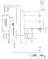
- FIG. 3 illustrates a horizontal deflection circuit adapting a horizontal S-shaped correction signal circuit according to the present invention.
- HD denotes a horizontal driving signal generator
- T R denotes a horizontal output transistor
- D denotes a damper diode
- C r denotes an oscillation condenser
- L DY denotes a horizontal deflection coil
- C s denotes a main correction condenser
- FBT denotes a flyback transformer
- +B denotes a horizontal deflection circuit voltage.
- the s-shaped correction condenser C S is connected in parallel with a front (rear) portion correction condenser C S1 and a rear (front) portion correction condenser C S2 for changing the capacitance thereof and switches SW 1 and SW 2 for switching the condensers C S1 and S S2 , respectively.
- a discharging high resistance (high resistance; not shown) is connected in parallel with the correction condensers C S1 and C S2 .
- Each of the switches SW 1 and SW 2 is composed of a field effect transistor (FET) which is turned on and off in accordance with respective first and second control signals CS-C TL1 and CS-C TL2 generated by a timing pulse generator 11.
- FET field effect transistor
- a wave form shaping unit 12 receives a flyback pulse signal from an auxiliary winding 13 of the flyback transformer FBT and outputs a shaped signal to the timing pulse generator 11, which also receives a vertical parabola signal and a pair of control signals DA-CT L1 and DA-CT L2 .
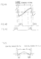
- Figure 4A illustrates a current flowing in the deflection yoke
- Figure 4B illustrates a first control signal CS-C TL1
- Figure 4C illustrates a second control signal CS-C TL2 .
- the first control signal CS-C TL1 is outputted, and the switch SW 1 is turned on.
- a second control signal CS-C TL2 is outputted, whereby the switch SW 2 is operated. Therefore, during the time interval t1 of the front portion of the horizontal scanning interval, the correction condenser C S is connected in parallel with the front portion correction condenser C S1 . Thereafter, the front correction S-shaped condenser C S1 is disconnected, and only the S-shaped condenser C S is connected. At the time t2 in the rear portion, the correction condenser C S is parallely connected with the rear portion correction condenser C S2 .
- Figure 5 illustrates the wave form of a voltage signal applied to the S-shaped signal correction condenser C S .
- the straight line characteristic is changed to the broken line characteristic.
- the capacitance of the S-shaped correction signal condenser is changed, and thus the oscillation frequency of the horizontal deflection signal L DY is changed.
- the characteristic of the correction condenser is changed by controlling the parallel connection of the correction C S1 and C S2 in the front and rear portions of the horizontal scan by controlling the time intervals of the first and second control signals CS-C TL1 and CS-C TL2 , so that it is possible to correct the horizontal distortion of the image and obtain accuracy thereof.
- the timing pulse generator 11 receives a saw tooth wave form signal as an FBT pulse from the auxiliary winding 13 of the flyback transformer FBT passes through the wave form shaping unit 12, the vertical parabola wave signal which is used in the circuit of the cathode ray tube, and direct current control signals DA-C TL1 and DA-C TL2 outputted to externally connected elements such as a microcomputer, etc.
- the timing pulse generator 11 includes first and second direct current voltage adders 15 and 16, first and second comparators 17 and 18, and an inverting amplifier 19.
- the first direct current voltage adder 15 receives the vertical parabola wave signal and first direct current control signal DA-C TL1 .
- the second direct current voltage adder 16 receives the vertical parabola wave signal and second control direct current signal DA-C TL2 .
- the comparator 17 receives the saw tooth wave form signal the polarity of which is inverted by the inverting amplifier 19 and an output signal from the first direct current voltage adder 15, respectively, and outputs the first control signal CS-C TL1 .
- the second comparator 18 receives the saw tooth wave form signal and an output signal from the second direct current voltage adder 16 and outputs the second control signal CS-C TL2 , respectively.
- timing pulse generator 11 The operation of the timing pulse generator 11 will be explained with reference to Figures 7A-7D and 8A-8D.
- the wave form shown in Figure 7A corresponds to the input signals to the second comparator 18 and denotes the interrelationship between the vertical parabola wave form of one field and the saw tooth wave signal.
- the vertical parabola wave signal is combined with the direct current control signal DA-C TL2 by the second direct current voltage adder 16.
- the portion A denotes the value of the vertical parabola wave signal at the upper vertical screen position of the cathode ray tube
- the portion B denotes the value of the vertical parabola wave signal at the center vertical screen position of the cathode ray tube
- the portion C denotes the value of the vertical parabola wave signal at the lower vertical screen position of the cathode ray tube.
- the wave form shown in Figure 7B is an enlarged view of the wave form shown in Figure 7A showing one horizontal scanning period.
- the values at the portions A, C and B of the wave form shown in Figure 7A correspond to the vertical parabola wave.
- the second comparator 18 outputs second control signal CS-CT TL2 when the value of the saw tooth wave exceeds the value of the vertical parabola wave signal.
- the wave form of the second control signal CS-C TL2 is shown in Figures 7C and 7D and corresponds to the control signal of the rear portion of the horizontal scanning interval.
- the output period of the control signal CS-C TL2 is shortened.
- the output interval of the control signal CS-C TL2 is extended.
- the wave form shown in Figure 8A corresponds to the input signals to the first comparator 17 and denotes the interrelationship between the vertical parabola wave signal of one field and the saw tooth wave signal.
- the saw tooth wave signal is inverted by the inverting amplifier 19, and the vertical parabola wave signal is combined with the direct current control signal DA-C TL2 by the first direct current voltage adder 15, respectively.
- the portions A', B' and C' are the same as the portions A, B and C shown in Figure 7A.
- the wave form shown in Figure 8B is an enlarged view of the wave form shown in Figure 8A for one horizontal scanning period.
- the first comparator 18 outputs the control signal CS-C TL1 when the value of the vertical parabola wave signal exceeds the value of the saw tooth wave signal, identically to the second comparator 18. Therefore, the output signal CS-C TL1 as shown in Figures 8C and 8D becomes the control signals at the front portion of the horizontal scanning interval.
- Figure 9 illustrates the effects of the variations in the pulse widths of the first and second control signals CS-C TL1 and CS-C TL2 during a vertical scanning period or a screen 21 of the cathode ray tube.
- the arrows denote the pulse widths of the control signals CS-C TL1 and CS-C TL2 during a horizontal scanning period.
- the pulse widths of the control signals are wider at the upper and lower portions A and C of the cathode ray tube 21, and narrower at the central portion of the same.
- the range of the non-spherical surface distortion which occurs in the left and right portions (edges) in the horizontal direction of the cathode ray tube is increased at the upper and lower portions (edges) of the cathode ray tube, and is more decreased toward the central portion.
- the pulse widths for which the correction is performed is varied based on the range of the distortion, it is possible to implement a better correction.
- the values of the direct current control signals DA-C TL1 and DA-C TL2 are controlled by a microcomputer, etc., as the values of the vertical parabola wave signal shown in Figures 7B and 8B are increased, so that the pulse widths of the control signals from the first and second comparators 17 and 18 can be varied. Therefore, the values of the first and second direct current control signals DA-C TL1 and Da-C TL2 are corrected, and thus the S-shape correction characteristic is adjusted.
- the first and second switching means for varying, for example, the number of the switchable correction condensers may be changed, and the interval of their switching may be changed.
- the first and second direct current voltage adders 15 and 16 may be omitted.
- One of the direct current control signals DA-C TL1 and DA-C TL2 or the vertical parabola wave signal may be inputted into the first and second comparators 17 and 18, for thus being compared with the value of the saw tooth wave signal.
- the signal value used for comparing with the value of the saw tooth wave signal may be a fixed value.
Landscapes
- Engineering & Computer Science (AREA)
- Multimedia (AREA)
- Signal Processing (AREA)
- Details Of Television Scanning (AREA)
Applications Claiming Priority (3)
| Application Number | Priority Date | Filing Date | Title |
|---|---|---|---|
| JP8313770A JPH10164388A (ja) | 1996-11-25 | 1996-11-25 | 水平s字補正回路 |
| JP313770/96 | 1996-11-25 | ||
| US08/975,597 US5955848A (en) | 1996-11-25 | 1997-11-21 | Horizontal deflection S-shaped correction signal circuit with variable capacitance |
Publications (2)
| Publication Number | Publication Date |
|---|---|
| EP0844786A1 true EP0844786A1 (fr) | 1998-05-27 |
| EP0844786B1 EP0844786B1 (fr) | 2006-04-05 |
Family
ID=26567701
Family Applications (1)
| Application Number | Title | Priority Date | Filing Date |
|---|---|---|---|
| EP97402809A Expired - Lifetime EP0844786B1 (fr) | 1996-11-25 | 1997-11-21 | Circuit pour la correction en S de la déflection horizontale avec capacité variable |
Country Status (4)
| Country | Link |
|---|---|
| US (1) | US5955848A (fr) |
| EP (1) | EP0844786B1 (fr) |
| JP (1) | JPH10164388A (fr) |
| CN (1) | CN1134151C (fr) |
Cited By (2)
| Publication number | Priority date | Publication date | Assignee | Title |
|---|---|---|---|---|
| EP1742460A1 (fr) * | 2005-06-18 | 2007-01-10 | TTE Germany GmbH | Circuit de correction de distorsion de trame |
| EP1836839A4 (fr) * | 2004-12-17 | 2010-07-21 | Lg Electronics Inc | Circuit de polarisation et procede de fonctionnement |
Families Citing this family (4)
| Publication number | Priority date | Publication date | Assignee | Title |
|---|---|---|---|---|
| KR200244058Y1 (ko) * | 1998-02-26 | 2001-09-29 | 윤종용 | 수평편향 회로의 방전회로 |
| JPH11355601A (ja) * | 1998-06-05 | 1999-12-24 | Sony Corp | 水平偏向回路 |
| KR100672412B1 (ko) * | 2004-12-17 | 2007-01-24 | 엘지전자 주식회사 | 화면 왜곡 보상 시스템 및 그 구동방법 |
| KR100671204B1 (ko) * | 2005-03-08 | 2007-01-19 | 삼성전자주식회사 | 다이나믹 포커스 제어장치 |
Citations (2)
| Publication number | Priority date | Publication date | Assignee | Title |
|---|---|---|---|---|
| EP0146345A2 (fr) * | 1983-12-16 | 1985-06-26 | Rca Licensing Corporation | Circuit de correction en "S" à capacité commutée |
| US5530488A (en) * | 1991-11-02 | 1996-06-25 | Rilly; Gerard | Circuit for the continuous zoom adjustment of the picture width in a television receiver |
Family Cites Families (8)
| Publication number | Priority date | Publication date | Assignee | Title |
|---|---|---|---|---|
| US4501995A (en) * | 1982-04-06 | 1985-02-26 | Tektronix, Inc. | Automatic "S" correction circuit |
| JPH0646786B2 (ja) * | 1985-04-19 | 1994-06-15 | ソニー株式会社 | マルチ走査形テレビジヨン受像機の水平偏向回路 |
| US4645985A (en) * | 1986-02-26 | 1987-02-24 | Rca Corporation | S-correction circuit for a video display |
| US4709193A (en) * | 1986-05-30 | 1987-11-24 | Rca Corporation | S-capacitance switching circuit for a video display |
| JPH0748805B2 (ja) * | 1990-05-28 | 1995-05-24 | 三菱電機株式会社 | オート・トラッキング・モニタのs字補正コンデンサ切替装置 |
| JPH04324763A (ja) * | 1991-04-24 | 1992-11-13 | Mitsubishi Electric Corp | オートスキャン水平偏向装置 |
| KR100342295B1 (ko) * | 1994-08-18 | 2002-11-23 | 코닌클리케 필립스 일렉트로닉스 엔.브이. | 에스보정캐패시터용스위칭장치및화상디스플레이장치 |
| FR2738976A1 (fr) * | 1995-09-20 | 1997-03-21 | Philips Electronics Nv | Circuit de balayage horizontal de television muni d'une capacite de s commutee par un thyristor |
-
1996
- 1996-11-25 JP JP8313770A patent/JPH10164388A/ja active Pending
-
1997
- 1997-11-21 US US08/975,597 patent/US5955848A/en not_active Expired - Fee Related
- 1997-11-21 EP EP97402809A patent/EP0844786B1/fr not_active Expired - Lifetime
- 1997-11-25 CN CNB971221723A patent/CN1134151C/zh not_active Expired - Fee Related
Patent Citations (2)
| Publication number | Priority date | Publication date | Assignee | Title |
|---|---|---|---|---|
| EP0146345A2 (fr) * | 1983-12-16 | 1985-06-26 | Rca Licensing Corporation | Circuit de correction en "S" à capacité commutée |
| US5530488A (en) * | 1991-11-02 | 1996-06-25 | Rilly; Gerard | Circuit for the continuous zoom adjustment of the picture width in a television receiver |
Cited By (2)
| Publication number | Priority date | Publication date | Assignee | Title |
|---|---|---|---|---|
| EP1836839A4 (fr) * | 2004-12-17 | 2010-07-21 | Lg Electronics Inc | Circuit de polarisation et procede de fonctionnement |
| EP1742460A1 (fr) * | 2005-06-18 | 2007-01-10 | TTE Germany GmbH | Circuit de correction de distorsion de trame |
Also Published As
| Publication number | Publication date |
|---|---|
| CN1185696A (zh) | 1998-06-24 |
| EP0844786B1 (fr) | 2006-04-05 |
| CN1134151C (zh) | 2004-01-07 |
| JPH10164388A (ja) | 1998-06-19 |
| US5955848A (en) | 1999-09-21 |
Similar Documents
| Publication | Publication Date | Title |
|---|---|---|
| US4139799A (en) | Convergence device for color television receiver | |
| US5955848A (en) | Horizontal deflection S-shaped correction signal circuit with variable capacitance | |
| KR100374053B1 (ko) | 내측래스터왜곡보정회로 | |
| KR100266585B1 (ko) | 수평에스자보정회로 | |
| US5508593A (en) | Differential error convergence correction | |
| US3968403A (en) | Circuit for correcting deflection distortion | |
| KR0122947Y1 (ko) | 와이드 티브이 수상기의 직선성 보정회로 | |
| EP0487795B1 (fr) | Appareil pour la correction de linearité | |
| JPH08321966A (ja) | モニターのチルト補正回路 | |
| EP0950314B1 (fr) | Generateur de tension de focalisation de faisceau d'electrons | |
| JP2992288B2 (ja) | ディスプレイ装置 | |
| JP3077159B2 (ja) | ダイナミックフォーカス回路 | |
| KR100425804B1 (ko) | 우측에지차동오차의수렴보정회로 | |
| KR100248720B1 (ko) | 광스크린의 종횡비변경 제어회로 | |
| EP0743797A2 (fr) | Correction de convergence différentielle du bord droit | |
| JP2919822B2 (ja) | ディスプレイ装置 | |
| JP2835035B2 (ja) | ディスプレイ装置 | |
| JPH09163392A (ja) | 右エッジずれ誤差の収束補正 | |
| JPH08163391A (ja) | 垂直偏向回路 | |
| JP2000295491A (ja) | 水平直線性補正回路 | |
| JPH0584701B2 (fr) | ||
| JPS62168494A (ja) | ダイナミツク・コンバ−ゼンス補正装置 | |
| KR19990002374U (ko) | 모니터에 있어서 3채널 s보정 커패시터 스위칭회로 | |
| JPH06261220A (ja) | 垂直偏向回路 | |
| JPH06225173A (ja) | 直線性歪補正回路 |
Legal Events
| Date | Code | Title | Description |
|---|---|---|---|
| PUAI | Public reference made under article 153(3) epc to a published international application that has entered the european phase |
Free format text: ORIGINAL CODE: 0009012 |
|
| AK | Designated contracting states |
Kind code of ref document: A1 Designated state(s): DE FR GB |
|
| AX | Request for extension of the european patent |
Free format text: AL;LT;LV;MK;RO;SI |
|
| 17P | Request for examination filed |
Effective date: 19980911 |
|
| AKX | Designation fees paid |
Free format text: DE FR GB |
|
| RBV | Designated contracting states (corrected) |
Designated state(s): DE FR GB |
|
| 17Q | First examination report despatched |
Effective date: 20031216 |
|
| GRAP | Despatch of communication of intention to grant a patent |
Free format text: ORIGINAL CODE: EPIDOSNIGR1 |
|
| GRAS | Grant fee paid |
Free format text: ORIGINAL CODE: EPIDOSNIGR3 |
|
| GRAA | (expected) grant |
Free format text: ORIGINAL CODE: 0009210 |
|
| AK | Designated contracting states |
Kind code of ref document: B1 Designated state(s): DE FR GB |
|
| REG | Reference to a national code |
Ref country code: GB Ref legal event code: FG4D |
|
| REF | Corresponds to: |
Ref document number: 69735616 Country of ref document: DE Date of ref document: 20060518 Kind code of ref document: P |
|
| ET | Fr: translation filed | ||
| PLBE | No opposition filed within time limit |
Free format text: ORIGINAL CODE: 0009261 |
|
| STAA | Information on the status of an ep patent application or granted ep patent |
Free format text: STATUS: NO OPPOSITION FILED WITHIN TIME LIMIT |
|
| 26N | No opposition filed |
Effective date: 20070108 |
|
| PGFP | Annual fee paid to national office [announced via postgrant information from national office to epo] |
Ref country code: DE Payment date: 20071115 Year of fee payment: 11 |
|
| PGFP | Annual fee paid to national office [announced via postgrant information from national office to epo] |
Ref country code: GB Payment date: 20071121 Year of fee payment: 11 Ref country code: FR Payment date: 20071108 Year of fee payment: 11 |
|
| GBPC | Gb: european patent ceased through non-payment of renewal fee |
Effective date: 20081121 |
|
| REG | Reference to a national code |
Ref country code: FR Ref legal event code: ST Effective date: 20090731 |
|
| PG25 | Lapsed in a contracting state [announced via postgrant information from national office to epo] |
Ref country code: DE Free format text: LAPSE BECAUSE OF NON-PAYMENT OF DUE FEES Effective date: 20090603 |
|
| PG25 | Lapsed in a contracting state [announced via postgrant information from national office to epo] |
Ref country code: GB Free format text: LAPSE BECAUSE OF NON-PAYMENT OF DUE FEES Effective date: 20081121 |
|
| PG25 | Lapsed in a contracting state [announced via postgrant information from national office to epo] |
Ref country code: FR Free format text: LAPSE BECAUSE OF NON-PAYMENT OF DUE FEES Effective date: 20081130 |