EP0845546A2 - Heisswand-Reaktionskammer und ihre Verwendung in einer Methode zur Herstellung einer Halbkugel-Korn-Schicht - Google Patents
Heisswand-Reaktionskammer und ihre Verwendung in einer Methode zur Herstellung einer Halbkugel-Korn-Schicht Download PDFInfo
- Publication number
- EP0845546A2 EP0845546A2 EP97307402A EP97307402A EP0845546A2 EP 0845546 A2 EP0845546 A2 EP 0845546A2 EP 97307402 A EP97307402 A EP 97307402A EP 97307402 A EP97307402 A EP 97307402A EP 0845546 A2 EP0845546 A2 EP 0845546A2
- Authority
- EP
- European Patent Office
- Prior art keywords
- reaction chamber
- forming
- silicon layer
- hsg silicon
- hsg
- Prior art date
- Legal status (The legal status is an assumption and is not a legal conclusion. Google has not performed a legal analysis and makes no representation as to the accuracy of the status listed.)
- Withdrawn
Links
Images


Classifications
-
- H—ELECTRICITY
- H10—SEMICONDUCTOR DEVICES; ELECTRIC SOLID-STATE DEVICES NOT OTHERWISE PROVIDED FOR
- H10B—ELECTRONIC MEMORY DEVICES
- H10B12/00—Dynamic random access memory [DRAM] devices
-
- H—ELECTRICITY
- H10—SEMICONDUCTOR DEVICES; ELECTRIC SOLID-STATE DEVICES NOT OTHERWISE PROVIDED FOR
- H10D—INORGANIC ELECTRIC SEMICONDUCTOR DEVICES
- H10D1/00—Resistors, capacitors or inductors
- H10D1/60—Capacitors
- H10D1/68—Capacitors having no potential barriers
- H10D1/692—Electrodes
- H10D1/711—Electrodes having non-planar surfaces, e.g. formed by texturisation
- H10D1/712—Electrodes having non-planar surfaces, e.g. formed by texturisation being rough surfaces, e.g. using hemispherical grains
-
- C—CHEMISTRY; METALLURGY
- C23—COATING METALLIC MATERIAL; COATING MATERIAL WITH METALLIC MATERIAL; CHEMICAL SURFACE TREATMENT; DIFFUSION TREATMENT OF METALLIC MATERIAL; COATING BY VACUUM EVAPORATION, BY SPUTTERING, BY ION IMPLANTATION OR BY CHEMICAL VAPOUR DEPOSITION, IN GENERAL; INHIBITING CORROSION OF METALLIC MATERIAL OR INCRUSTATION IN GENERAL
- C23C—COATING METALLIC MATERIAL; COATING MATERIAL WITH METALLIC MATERIAL; SURFACE TREATMENT OF METALLIC MATERIAL BY DIFFUSION INTO THE SURFACE, BY CHEMICAL CONVERSION OR SUBSTITUTION; COATING BY VACUUM EVAPORATION, BY SPUTTERING, BY ION IMPLANTATION OR BY CHEMICAL VAPOUR DEPOSITION, IN GENERAL
- C23C16/00—Chemical coating by decomposition of gaseous compounds, without leaving reaction products of surface material in the coating, i.e. chemical vapour deposition [CVD] processes
- C23C16/22—Chemical coating by decomposition of gaseous compounds, without leaving reaction products of surface material in the coating, i.e. chemical vapour deposition [CVD] processes characterised by the deposition of inorganic material, other than metallic material
- C23C16/24—Deposition of silicon only
-
- C—CHEMISTRY; METALLURGY
- C23—COATING METALLIC MATERIAL; COATING MATERIAL WITH METALLIC MATERIAL; CHEMICAL SURFACE TREATMENT; DIFFUSION TREATMENT OF METALLIC MATERIAL; COATING BY VACUUM EVAPORATION, BY SPUTTERING, BY ION IMPLANTATION OR BY CHEMICAL VAPOUR DEPOSITION, IN GENERAL; INHIBITING CORROSION OF METALLIC MATERIAL OR INCRUSTATION IN GENERAL
- C23C—COATING METALLIC MATERIAL; COATING MATERIAL WITH METALLIC MATERIAL; SURFACE TREATMENT OF METALLIC MATERIAL BY DIFFUSION INTO THE SURFACE, BY CHEMICAL CONVERSION OR SUBSTITUTION; COATING BY VACUUM EVAPORATION, BY SPUTTERING, BY ION IMPLANTATION OR BY CHEMICAL VAPOUR DEPOSITION, IN GENERAL
- C23C16/00—Chemical coating by decomposition of gaseous compounds, without leaving reaction products of surface material in the coating, i.e. chemical vapour deposition [CVD] processes
- C23C16/44—Chemical coating by decomposition of gaseous compounds, without leaving reaction products of surface material in the coating, i.e. chemical vapour deposition [CVD] processes characterised by the method of coating
- C23C16/46—Chemical coating by decomposition of gaseous compounds, without leaving reaction products of surface material in the coating, i.e. chemical vapour deposition [CVD] processes characterised by the method of coating characterised by the method used for heating the substrate
-
- H—ELECTRICITY
- H10—SEMICONDUCTOR DEVICES; ELECTRIC SOLID-STATE DEVICES NOT OTHERWISE PROVIDED FOR
- H10P—GENERIC PROCESSES OR APPARATUS FOR THE MANUFACTURE OR TREATMENT OF DEVICES COVERED BY CLASS H10
- H10P14/00—Formation of materials, e.g. in the shape of layers or pillars
- H10P14/20—Formation of materials, e.g. in the shape of layers or pillars of semiconductor materials
Definitions
- the present invention relates to a reaction chamber portion and a method for forming an HSG silicon layer using the same, and more particularly, to a warm wall type reaction chamber portion and a method for forming an HSG silicon layer using the same.
- a capacitor which is one component of a semiconductor device
- a high dielectric film such as BST((Ba, Sr)TiO 3 ) and PZT(Pb(Zr, Ti)O 3 ) may be used.
- the high dielectric films have been of only partial use, and only in certain applications.
- a cylindrical, stack- or fin-type capacitor electrode has been developed, instead of the conventional planar-type electrode.
- a method for forming a hemi-spherical grain (HSG) silicon layer on an electrode surface of a capacitor is widely used, to increase the effective area of the electrode.
- the selectivity loss margin is the degree to which HSG silicon layer forms on an oxide layer, during forming HSG silicon layer on a silicon electrode.
- An inner wall of the cold wall type reaction chamber is at a temperature of 10°C ⁇ 20°C, to prevent reaction gas from being adsorbed on the inner wall.
- FIGS. 1 and 2 are views showing this conventional method for manufacturing a capacitor.
- a gate electrode (not shown) is formed on a semiconductor substrate 10, and then a conductive impurity layer is formed on the substrate 10 using the gate electrode as a mask, to form a transistor.
- an interlayer dielectric film 12 is patterned to form a contact hole 14 for exposing part of the semiconductor substrate 10, on the entire surface of the semiconductor substrate 10 where the transistor is formed.
- the conductive material layer filling the contact hole 14 is formed on the entire surface of the interlayer dielectric film 12, and then the conductive material layer is patterned, to form a conductive layer pattern 16 corresponding to a storage node of a capacitor.
- the resultant structure is transferred to the cold wall reaction chamber, where an HSG silicon layer 18 is formed on the surface of the conductive layer pattern 16.
- the cold wall type reaction chamber includes a susceptor whereon the semiconductor substrate 10 is loaded.
- the susceptor is heated to approximately 600°C before the substrate is loaded. This is a temperature appropriate for forming the HSG silicon layer.
- the substrate 10 is loaded on the susceptor, and then reaction gas for forming an HSG seed is supplied into the reaction chamber during a process of stabilization.
- the reaction gas is one selected from the group consisting of silane SiH 4 and disilane Si 2 H 6 .
- the HSG seeding is formed by the reaction gas, on the entire surface of the structure where the conductive layer pattern 16 is formed. Then, the HSG seed is grown through an annealing process to form an HSG silicon layer. Referring to FIG. 1, a first HSG silicon layer 18 is formed on the surface of the conductive layer pattern 16. A second HSG silicon layer 20, having a size smaller than that of the first HSG silicon layer 18, is formed on the entire surface of the interlayer dielectric film 12. It is preferable that the HSG silicon layer is formed only on the conductive layer pattern 16. Therefore, the entire surface of the resultant structure is etched back. As shown in FIG. 2, after the etchback, a first HSG silicon layer pattern 18a, having a unit area smaller than that of the first HSG silicon layer 18 formed on the side wall of the conductive layer pattern 16, is formed on the upper portion of the conductive layer pattern 16.
- the conventional method for forming a capacitor having an HSG silicon layer includes an etch-back process, so that the surface area of the HSG silicon layer formed on a surface of the conductive layer pattern is reduced, which leads to a reduction in capacitance.
- cooling water flows in the inner wall of the cold wall type reaction chamber. Accordingly, when the reaction gas of the reaction chamber portion reaches the substrate, the temperature of the reaction gas is lower than that of the substrate. Therefore, a relatively long time is required to increase the temperature of the reaction gas to the temperature of the substrate to allow the reaction gas to react with the substrate. As a result, in the case that the HSG silicon layer is formed using the cold wall type reaction chamber, much time is required for forming the HSG.
- a reaction chamber comprising a susceptor where a heater for heating a substrate is installed, and an adiabatic unit surrounding a wall of the reaction chamber. At this time, the wall has a temperature of approximately 200 ⁇ 500°C.
- the adiabatic unit is a silicon carbide heater having coils as a heat generator.
- the wall is a quartz tube and a silicon carbide tube surrounding the quartz tube.
- the reaction gas is one selected from a group consisting of SiH 4 , Si 2 H 6 and DCS which are gases for forming an HSG seed.
- a method for forming HSG of a semiconductor device which comprises the steps of:
- a reaction chamber having the adiabatic unit surrounding the wall of the reaction chamber is used as the warm wall type reaction chamber.
- an HSG silicon layer without damage or defects can be formed on a lower electrode of the capacitor, and also, time for forming an HSG is reduced, to increase manufacturing productivity of a semiconductor device.
- FIGS. 1 and 2 are views sequentially showing a conventional method for fabricating a capacitor of a semiconductor device
- FIG. 3 is a sectional view of a warm wall type reaction chamber according to an embodiment of the present invention.
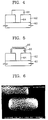
- FIGS. 4 and 5 are views sequentially showing a method for manufacturing a capacitor of a semiconductor device using the warm wall type reaction chamber of FIG. 3;
- FIG. 6 is a SEM phohotograph of an HSG silicon layer formed by the method for fabricating the capacitor of a semiconductor device using the warm wall type reaction chamber of FIG. 3;
- FIGS. 7 and 8 are graphs showing temperature change according to time during a process of forming an HSG silicon layer by a conventional art and according to the present invention, respectively.
- the warm wall type reaction chamber portion shown in FIG. 3 includes a reaction chamber and an adiabatic unit surrounding the reaction chamber.
- the reaction chamber includes an inner wall formed of a quartz tube 46 and an outer wall formed of a silicon carbide tube 50.
- a susceptor 40 where a substrate 44 is mounted is located in the reaction chamber.
- a heater 42 for heating the substrate 44 is installed in the susceptor 40.
- the reaction gas is for forming HSG silicon layer, and is at least one selected from the group consisting of silane (SiH 4 ), disilane (Si 2 H 6 ) and Dichloro silane (DCS).
- An outlet 49 for discharging reacted gas in the reaction chamber is formed to the right side of the susceptor 40. Since the outlet 49 is connected to a pumping unit (not shown), the inside of the reaction chamber can be maintained at a desired pressure.
- a load-lock chamber 51 for loading or unloading the substrate 44, is connected in one side of the reaction chamber portion, and the load-lock chamber 51 is connected to a transfer chamber (not shown).
- An O-ring 48 is installed between the quartz tube 46 and a lower structure with which the quartz tube 46 contacts.
- the adiabatic unit 52 surrounding the silicon carbide tube 50, has a heating coil 54 therein. The heating coil 54 constantly maintains the temperature of the inside of the reaction chamber.
- a method, for fabricating a capacitor having an HSG silicon layer formed on an electrode surface, will be described using a warm wall type reaction chamber portion having the above structure.
- a transistor(not shown) is formed on an active region of a semiconductor substrate 60.
- An interlayer dielectric film 62 is formed on the entire surface of the semiconductor substrate 60 where the transistor is formed, and patterned to form a contact hole 64 for partially exposing the semiconductor substrate 60.
- a conductive material layer for filling the contact hole 64 is formed on the entire surface of the interlayer dielectric film 62.
- the conductive material layer is formed of an amorphous silicon layer.
- the conductive material layer is patterned to form a conductive layer pattern 66 for filling the contact hole 64.
- the conductive layer pattern 66 acts as a storage node of a capacitor.
- FIG. 5 shows a step of forming an HSG silicon layer 68.
- the resultant structure where the conductive layer pattern 66 is formed is loaded into a warm wall type reaction chamber.
- the HSG silicon layer 68 is formed on the surface of the conductive layer pattern 66.
- a selective deposition process is performed in which an HSG silicon layer is formed only on the silicon, to thereby form a uniform HSG silicon layer on the entire surface of the conductive layer pattern 66.
- the semiconductor substrate 44 of FIG. 3 is the semiconductor substrate 60 where the conductive layer pattern 66 is formed, as shown in FIG. 4.
- the substrate 44 where the conductive layer pattern 60 is formed, is loaded on the susceptor 40, through the load-lock chamber 51 of the warm wall type reaction chamber portion having the above structure.
- the temperature of the susceptor 40 is maintained at 560 ⁇ 630°C by a silicon carbide heater 42 installed in the susceptor 40. Accordingly, after the substrate 44 is loaded on the susceptor 40, the temperature of the substrate 44 matches that of the susceptor 40.
- reaction gas is supplied into the reaction chamber through the gas supply tube 47, in such a state that temperatures of the quartz tube 46 and the silicon carbide tube 50 are maintained at 200 ⁇ 500°C.
- the reaction gas for forming an HSG seed is one selected from the group consisting of silane, disilane and DCS.
- the inside of the reaction chamber is maintained at a pressure of several millitorr to several tens of millitorr.
- the silicon carbide tube 50 must be maintained at a temperature equal to that of the quartz tube 46. This is performed by installing a heater on each tube 46 and 50, or by using the tubes 46 and 50 formed of a black body, to thereby prevent heat of the reaction chamber from being discharged.
- an adiabatic unit is formed surrounding the total external surface of the silicon carbide tube 50, to prevent heat loss from the reaction chamber, so that the inside of the reaction chamber is heated until the reaction gas injected into the reaction chamber reaches the substrate 44.
- the adiabatic unit 52 includes a silicon carbide heater for generating heat.
- FIG. 6 is an SEM photograph of HSG silicon layer selectively formed on the entire surface of the conductive layer pattern 66.
- the reaction gas Since the inside of the reaction chamber maintains at a temperature of 200 ⁇ 500°C, the reaction gas is heated to the above temperature before it reaches the substrate 60. Accordingly, it takes less time, than that in the conventional cold wall type chamber, for the reaction gas to attain the temperature of the substrate 44, after it reaches the substrate 44 to form a seed. That is, time for temperature stabilization is very short.
- the HSG silicon seed formed on the entire surface of the conductive layer pattern 66, is grown through annealing to form an HSG silicon layer 68 on the entire surface of the conductive layer pattern 66, as shown in FIG. 5.
- the HSG silicon layer 68 since the selective HSG silicon layer is formed by deposition, the HSG silicon layer 68 has little damage.
- a uniform HSG silicon layer 68 is formed on the entire surface of the conductive layer pattern 66.
- pressure in the reaction chamber is maintained at 1 x 10 -7 torr, which is lower than the pressure when the reaction gas is injected.
- the period of time for the reaction gas to attain the temperature of the substrate 44 can be reduced.
- the HSG silicon layer is formed by stabilizing the temperature of a substrate, supplying reaction gas into the reaction chamber to form an HSG silicon seed, and growing the HSG silicon seed.
- reference characters T1 and T1' indicate the time for stabilizing substrate temperature, by the conventional art and according to the present invention, respectively.
- reference characters T2 and T2' indicate the time for seeding and annealing, by the conventional art and according to the present invention, respectively.
- the time T1 for stabilizing a substrate in a conventional cold wall type reaction chamber is longer than the time T1' for a warm wall type reaction chamber portion according to the present invention. Also, by the conventional art, the temperature is unstable during the stabilization step.
- the total time for the stabilizing process and forming the HSG silicon layer through annealing is approximately 8min, while it is 12min in the conventional cold wall type reaction chamber. Therefore, productivity is enhanced.
- the temperature in the reaction chamber is maintained at 200 ⁇ 500°C, and an adiabatic unit is used for preventing heat discharge from the reaction chamber, to selectively form HSG on the surface of a storage electrode and reduce process time for forming the HSG silicon seed and the HSG silicon layer. Accordingly, productivity of manufacturing a semiconductor device having the HSG silicon layer can be enhanced.
Landscapes
- Chemical & Material Sciences (AREA)
- Metallurgy (AREA)
- Chemical Kinetics & Catalysis (AREA)
- Engineering & Computer Science (AREA)
- Materials Engineering (AREA)
- Mechanical Engineering (AREA)
- General Chemical & Material Sciences (AREA)
- Organic Chemistry (AREA)
- Inorganic Chemistry (AREA)
- Chemical Vapour Deposition (AREA)
- Semiconductor Integrated Circuits (AREA)
- Semiconductor Memories (AREA)
- Silicon Compounds (AREA)
- Battery Electrode And Active Subsutance (AREA)
Applications Claiming Priority (2)
| Application Number | Priority Date | Filing Date | Title |
|---|---|---|---|
| KR1019960060521A KR100224727B1 (ko) | 1996-11-30 | 1996-11-30 | 웜웰형 반응챔버 및 이를 이용한 커패시터 제조방법 |
| KR9660521 | 1996-11-30 |
Publications (2)
| Publication Number | Publication Date |
|---|---|
| EP0845546A2 true EP0845546A2 (de) | 1998-06-03 |
| EP0845546A3 EP0845546A3 (de) | 1999-12-15 |
Family
ID=19485135
Family Applications (1)
| Application Number | Title | Priority Date | Filing Date |
|---|---|---|---|
| EP97307402A Withdrawn EP0845546A3 (de) | 1996-11-30 | 1997-09-23 | Heisswand-Reaktionskammer und ihre Verwendung in einer Methode zur Herstellung einer Halbkugel-Korn-Schicht |
Country Status (4)
| Country | Link |
|---|---|
| EP (1) | EP0845546A3 (de) |
| JP (1) | JPH10163432A (de) |
| KR (1) | KR100224727B1 (de) |
| TW (1) | TW403994B (de) |
Cited By (4)
| Publication number | Priority date | Publication date | Assignee | Title |
|---|---|---|---|---|
| FR2770027A1 (fr) * | 1997-10-18 | 1999-04-23 | United Microelectronics Corp | Procede de fabrication d'une structure en silicium a grains hemispheriques |
| US6660095B2 (en) * | 2001-01-15 | 2003-12-09 | Jusung Engineering Co., Ltd. | Single wafer LPCVD apparatus |
| US6838127B2 (en) * | 1999-10-01 | 2005-01-04 | Samsung Electronics Co., Ltd. | Method and apparatus for forming an HSG-Si layer on a wafer |
| WO2006036129A1 (en) * | 2004-09-29 | 2006-04-06 | National University Of Singapore | A temperature monitoring apparatus, system and method for monitoring the temperature of a reactant system |
Families Citing this family (3)
| Publication number | Priority date | Publication date | Assignee | Title |
|---|---|---|---|---|
| KR100768727B1 (ko) * | 2001-01-12 | 2007-10-19 | 주성엔지니어링(주) | 트렌치 내벽에만 선택적으로 HSG-Si를 형성시키는방법 |
| JP5797595B2 (ja) * | 2012-03-23 | 2015-10-21 | 東京エレクトロン株式会社 | 成膜装置のパーツ保護方法および成膜方法 |
| CN106947954B (zh) * | 2017-04-27 | 2019-06-18 | 京东方科技集团股份有限公司 | 一种气相沉积设备及薄膜的制备方法 |
Family Cites Families (5)
| Publication number | Priority date | Publication date | Assignee | Title |
|---|---|---|---|---|
| US5259883A (en) * | 1988-02-16 | 1993-11-09 | Kabushiki Kaisha Toshiba | Method of thermally processing semiconductor wafers and an apparatus therefor |
| JP3230836B2 (ja) * | 1992-04-09 | 2001-11-19 | 東京エレクトロン株式会社 | 熱処理装置 |
| JP3125121B2 (ja) * | 1993-09-17 | 2001-01-15 | 東京エレクトロン株式会社 | 枚葉式ホットウォール処理装置のクリーニング方法 |
| US5407534A (en) * | 1993-12-10 | 1995-04-18 | Micron Semiconductor, Inc. | Method to prepare hemi-spherical grain (HSG) silicon using a fluorine based gas mixture and high vacuum anneal |
| KR0165496B1 (ko) * | 1995-03-22 | 1998-12-15 | 윤종용 | 고집적 반도체장치의 캐패시터 제조방법 |
-
1996
- 1996-11-30 KR KR1019960060521A patent/KR100224727B1/ko not_active Expired - Fee Related
-
1997
- 1997-08-14 TW TW086111668A patent/TW403994B/zh not_active IP Right Cessation
- 1997-09-23 EP EP97307402A patent/EP0845546A3/de not_active Withdrawn
- 1997-12-01 JP JP9330560A patent/JPH10163432A/ja active Pending
Cited By (4)
| Publication number | Priority date | Publication date | Assignee | Title |
|---|---|---|---|---|
| FR2770027A1 (fr) * | 1997-10-18 | 1999-04-23 | United Microelectronics Corp | Procede de fabrication d'une structure en silicium a grains hemispheriques |
| US6838127B2 (en) * | 1999-10-01 | 2005-01-04 | Samsung Electronics Co., Ltd. | Method and apparatus for forming an HSG-Si layer on a wafer |
| US6660095B2 (en) * | 2001-01-15 | 2003-12-09 | Jusung Engineering Co., Ltd. | Single wafer LPCVD apparatus |
| WO2006036129A1 (en) * | 2004-09-29 | 2006-04-06 | National University Of Singapore | A temperature monitoring apparatus, system and method for monitoring the temperature of a reactant system |
Also Published As
| Publication number | Publication date |
|---|---|
| KR19980041242A (ko) | 1998-08-17 |
| JPH10163432A (ja) | 1998-06-19 |
| EP0845546A3 (de) | 1999-12-15 |
| TW403994B (en) | 2000-09-01 |
| KR100224727B1 (ko) | 1999-10-15 |
Similar Documents
| Publication | Publication Date | Title |
|---|---|---|
| US5998824A (en) | Capacitor structure having a lower electrode with a rough surface, a plurality of metal layers and a nitridation treated film | |
| EP0742847B1 (de) | Verfahren zum auftragen von wolframnitrid unter verwendung eines silicium enthaltenden gases | |
| US5352623A (en) | Method for manufacturing a semiconductor device | |
| US6864527B2 (en) | Capacitor having tantalum oxynitride film and method for making same | |
| US20050054198A1 (en) | Apparatus of chemical vapor deposition | |
| US5563090A (en) | Method for forming rugged tungsten film and method for fabricating semiconductor device utilizing the same | |
| US5821152A (en) | Methods of forming hemispherical grained silicon electrodes including multiple temperature steps | |
| GB2364825A (en) | A capacitor using a tantalum nitride dielectric | |
| US6159849A (en) | Methods of forming nitride dielectric layers having reduced exposure to oxygen | |
| EP0845546A2 (de) | Heisswand-Reaktionskammer und ihre Verwendung in einer Methode zur Herstellung einer Halbkugel-Korn-Schicht | |
| US6486022B2 (en) | Method of fabricating capacitors | |
| US20010014510A1 (en) | Method for manufacturing a capacitor for semiconductor devices | |
| US5885867A (en) | Methods of forming hemispherical grained silicon layers including anti-nucleation gases | |
| US6632721B1 (en) | Method of manufacturing semiconductor devices having capacitors with electrode including hemispherical grains | |
| KR20010102091A (ko) | 아날로그 회로용의 커패시터 및 그것의 제조 방법 | |
| US6358864B1 (en) | Method of fabricating an oxide/nitride multilayer structure for IC manufacture | |
| GB2365211A (en) | DRAM capacitor having a crystalline TaON dielectric | |
| US6265261B1 (en) | Semiconductor device and fabricating method therefor in which a netride layer in a capacitor is formed in a shortened time period | |
| US6417536B2 (en) | Semiconductor device with memory capacitor having an electrode of Si1-x Gex | |
| US6312987B1 (en) | Method for manufacturing semiconductor device having hemispherical grain polysilicon film | |
| US6764916B1 (en) | Manufacturing method for semiconductor device | |
| US20070042574A1 (en) | Method for manufacturing a semiconductor device | |
| US6245632B1 (en) | Variable temperature methods of forming hemispherical grained silicon (HSG-Si) layers | |
| KR100301037B1 (ko) | 선택증착공정에의한반구형그레인실리콘층을사용하는커패시터형성방법 | |
| JPH11145423A (ja) | 半導体装置の製造方法 |
Legal Events
| Date | Code | Title | Description |
|---|---|---|---|
| PUAI | Public reference made under article 153(3) epc to a published international application that has entered the european phase |
Free format text: ORIGINAL CODE: 0009012 |
|
| 17P | Request for examination filed |
Effective date: 19971008 |
|
| AK | Designated contracting states |
Kind code of ref document: A2 Designated state(s): DE FR GB NL |
|
| PUAL | Search report despatched |
Free format text: ORIGINAL CODE: 0009013 |
|
| AK | Designated contracting states |
Kind code of ref document: A3 Designated state(s): AT BE CH DE DK ES FI FR GB GR IE IT LI LU MC NL PT SE |
|
| AKX | Designation fees paid |
Free format text: DE FR GB NL |
|
| STAA | Information on the status of an ep patent application or granted ep patent |
Free format text: STATUS: THE APPLICATION IS DEEMED TO BE WITHDRAWN |
|
| 18D | Application deemed to be withdrawn |
Effective date: 20000616 |