EP0846291B1 - Prozessor mit befehlscachespeicher - Google Patents
Prozessor mit befehlscachespeicher Download PDFInfo
- Publication number
- EP0846291B1 EP0846291B1 EP97918302A EP97918302A EP0846291B1 EP 0846291 B1 EP0846291 B1 EP 0846291B1 EP 97918302 A EP97918302 A EP 97918302A EP 97918302 A EP97918302 A EP 97918302A EP 0846291 B1 EP0846291 B1 EP 0846291B1
- Authority
- EP
- European Patent Office
- Prior art keywords
- bits
- instruction
- output
- computer processor
- bit
- Prior art date
- Legal status (The legal status is an assumption and is not a legal conclusion. Google has not performed a legal analysis and makes no representation as to the accuracy of the status listed.)
- Expired - Lifetime
Links
Images



Classifications
-
- G—PHYSICS
- G06—COMPUTING OR CALCULATING; COUNTING
- G06F—ELECTRIC DIGITAL DATA PROCESSING
- G06F12/00—Accessing, addressing or allocating within memory systems or architectures
- G06F12/02—Addressing or allocation; Relocation
- G06F12/08—Addressing or allocation; Relocation in hierarchically structured memory systems, e.g. virtual memory systems
- G06F12/0802—Addressing of a memory level in which the access to the desired data or data block requires associative addressing means, e.g. caches
- G06F12/0893—Caches characterised by their organisation or structure
- G06F12/0895—Caches characterised by their organisation or structure of parts of caches, e.g. directory or tag array
Definitions
- the invention relates to a computer processor with an instruction cache and a method of generating instructions for such a computer processor.
- the invention relates more in particular to VLIW (Very Long Instruction Word) processors and in particular to instruction formats for such processors and an apparatus and method for processing such instruction formats.
- VLIW Very Long Instruction Word
- VLIW processors have instruction words including a plurality of issue slots.
- the processors also include a plurality of functional units.
- Each functional unit is for executing a set of operations of a given type.
- Each functional unit is RISC-like in that it can begin an instruction in each machine cycle in a pipe-lined manner.
- Each issue slot is for holding a respective operation. All of the operations in a same instruction word are to be begun in parallel on the functional unit in a single cycle of the processor.
- the VLIW implements fine-grained parallelism.
- an instruction on a VLIW machine typically includes a plurality of operations.
- each operation might be referred to as a separate instruction.
- each instruction is composed of operations or no-ops (dummy operations).
- VLIW processors use a memory device, such as a disk drive to store instruction streams for execution on the processor.
- a VLIW processor can also use caches, like conventional processors, to store pieces of the instruction streams with high bandwidth accessibility to the processor.
- the instruction in the VLIW machine is built up by a programmer or compiler out of these operations.
- the scheduling in the VLIW processor is software controlled.
- the VLIW processor can be compared with other types of parallel processors such as vector processors and superscalar processors as follows.
- Vector processors have single operations which are performed on multiple data items simultaneously.
- Superscalar processors implement fine-grained parallelism, like the VLIW processors, but unlike the VLIW processor, the superscalar processor schedules operations in hardware.
- the VLIW processor has aggravated problems with cache use.
- large code size causes cache misses, i.e. situations where needed instructions are not in cache.
- Large code size also requires a higher main memory bandwidth to transfer code from the main memory to the cache.
- a computer comprising an instruction cache, according to the preamble to claim 1, is known from the document US-A-5442760.
- This document discloses an instruction cache located between a decoding stage and a plurality of functional units executing in parallel multiple instructions.
- multiple instructions may be read out of the cache per access. Therefore, the bit pattern in the instruction cache is not a bit per bit copy of the instructions in the instruction memory.
- the invention provides for a computer processor as set forth in Claim 1.
- a shuffled bit stream is used which simplifies cache layout.
- the cache stores a shuffled instruction stream and multiplexes bits from storage means onto a bus so that the bits are deshuffled. A multiplicity of lines leading from the storage means to the bus.
- the lines do not cross each other.
- the invention also relates to a method as set forth in Claim 7.
- a compiled and linked object module produced by a compiler and/or linker and code is received for swizzling the compiled and linked software to produce a second object module.
- the second object module is suitable for being deswizzled upon reading from a cache memory using a cache structure whose output bus wires are not crossed.
- FIG. 1a shows the general structure of a processor according to the invention.
- a microprocessor according to the invention includes a CPU 102, an instruction cache 103, and a data cache 105.
- the CPU is connected to the caches by high bandwidth buses.
- the microprocessor also contains a memory 104 where an instruction stream is stored.
- the cache 103 is structured to have 512 bit double words.
- the individual bytes in the words are addressable, but the bits are not. Bytes are 8 bits long.
- the double words are accessible as a single word in a single clock cycle.
- the instruction stream is stored as instructions in a compressed format.
- the compressed format is used both in the memory 104 and in the cache 103.
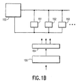
- Fig. 1b shows more detail of the VLIW processor according to the invention.
- the processor includes a multiport register file 150, a number of functional units 151, 152, 153, ..., and an instruction issue register 154, abbreviated IIR.
- the multiport register file stores results from and operands for the functional units.
- the instruction issue register includes a plurality of issue slots for containing operations to be commenced in a single clock cycle, in parallel, on the functional units 151, 152, 153, ..
- a decompression unit 155 converts the compressed instructions from the instruction cache 103 into a form usable by the IIR 154.
- a compressed instruction contains a format field which specifies which issue slots are to be used by the compressed instruction.
- format bits are stored in the instruction preceding the instruction to which the format bits relate. This allows pipelining of instruction retrieval.
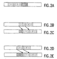
- Figs. 2a-2e show possible positions of instructions in cache.
- Fig. 3 shows a diagram of how source code becomes a loadable, compressed object module.
- First the source code 801 must be compiled by compiler 802 to create a first set of object modules 803. These modules are linked by linker 804 to create a second type of object module 805. This module is then compressed and shuffled at 806 to yield loadable module 807.
- Object modules II contain a number of standard data structures. These include: a header; global & local symbol tables; reference table for relocation information; a section table; and debug information, some of which are used by the compression and shuffling module 807.
- the object module II also has partitions, including a text partition, where the instructions to be processed reside, and a source partition which keeps track of which source files the text came from.
- FIG. 4 A high level flow chart of the compression and shuffling module is shown at Fig. 4.
- object module II is read in.
- the text partition is processed.
- the other sections are processed.
- the header is updated.
- the object module is output.
- Fig. 5 expands box 902.
- the reference table i.e. relocation information is gathered.
- the branch targets are collected, because these are not to be compressed.
- the software checks to see if there are more files in the source partition. If so, at 1004, the portion corresponding to the next file is retrieved. Then, at 1005, that portion is compressed. At 1006, file information in the source partition is updated. At 1007, the local symbol table is updated.
- the global symbol table is updated at 1008. Then, at 1009, address references in the text section are updated.
- the scatter table which is used as a result of the compression and shuffling of the invention, can be explained as follows.
- the reference table contains a list of locations of addresses used by the instruction stream and corresponding list of the actual addresses listed at those locations.
- the reference table is used at these times to allow the updating.
- the scatter table lists for each address in the reference table, where EACH BIT is located.
- the table lists a width of a bit field, an offset from the corresponding index of the address in the source text, a corresponding offset from the corresponding index in the address in the destination text.
- the scatter table allows the addresses listed in the reference table to be updated even before the bits are deshuffled.
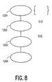
- Fig. 8 is a schematic of the decompression process. Instructions come from memory 1201, i.e. either from the main memory 104 or the instruction cache 105. The instructions must then be deshuffled 1201, which will be explained further below, before being decompressed 1203. After decompression 1203, the instructions can proceed to the CPU 1204.
- Fig. 6a shows the functioning on input of a cache structure which is useful in efficient processing of VLIW instructions.
- This cache includes 16 banks 601-616 of 2k bytes each. These banks share an input bus 617.
- the caches are divided into two stacks. The stack on the left will be referred to as “low” and the stack on the right will be referred to as "high”.
- the cache can take input in only one bank at a time and then only 4 bytes at a time. Addressing determines which 4 bytes of which bank are being filled. For each 512 bit word to be stored in the cache, 4 bytes are stored in each bank. A shaded portion of each bank is illustrated indicating corresponding portions of each bank for loading of a given word. These shaded portions are for illustration only. Any given word can be loaded into any set of corresponding portions of the banks.
- sequential 4 byte portions of the swizzled word are loaded into the banks in the following order 608, 616, 606, 614, 604, 612, 602, 610, 607, 615, 605, 613, 603, 611, 601, 609.
- the order of loading of the 4 byte sections of the swizzled word is indicated by roman numerals in the boxes representing the banks.
- Fig. 6b shows how the swizzled word is read out from the cache.
- Fig. 6b shows only the shaded portions of the banks of the low stack. The high portion is analogous.
- Each shaded portion 601a-608a has 32 bits.
- the bits are loaded onto the output bus, called bus256low using the connections shown, i.e. in the following order: 608a - bit0, 607a - bit 0, ..., 601a - bit 0; 608a - bit 1, 607a - bit, ..., 601a --bit 1; ...; 608a - bit 31, 607a - bit 31, ..., 601a - bit 31.
- the word is automatically deswizzled back to its proper bit order.
- the bundles of wires, 620, 621, ..., 622 together form the output bus256 low. These wires pass through the cache to the output without crossing.
- the cache looks like Fig. 7.
- the bits are read out from stack low 701 and stack high 702 under control of control unit 704 through a shift network 703 which assures that the bits are in the output order specified above. In this way the entire output of the 512 bit word is assured without bundles 620, 621, ... 622 and analogous wires crossing.
- the invention provides an instruction cache for use in a computer processor comprising means for storing respective bits of an instruction stream, which bits are preshuffled; and means for multiplexing bits from the storage means onto a bus so that the bits are deshuffled, which multiplexing means comprises a multiplicity of lines leading from the storage means to the bus, which lines do not cross each other.
- the instruction stream is in double word format; and the cache comprises a first stack for storing first words from the double word format and a second stack for storing second words from the double word format.
- the stacks are organized into banks and there is one bank for each bit of an output byte on the output bus.
- Multiplexer means is operative to transfer one bit from each bank in order to create an output byte.
- the cache is for storing n instructions, where n is an integer variable, and each bank contains at least one respective bit from each of the n instructions.
- Each bank contains a RAM column for each byte of an output word.
- the RAM columns are organized into m groups, where m is an integer representing a number of bytes in the output word, each respective group containing a respective RAM column for each bit of the output word, no two RAM columns in a single group being in a same bank.
- the multiplexer means comprises m column multiplexers, each column multiplexer being operative to multiplex a bit from each RAM column in the respective group into the output word.
- the instruction cache comprises first and second stacks of eight banks, each bank comprising 8 RAM columns of 1-bit 64 RAM cells, the RAM columns being organized into groups of 8 RAM columns, the first stack being for storing lower order bits of a double-word output, the second stack being for storing higher order bits of the double word output.
- the multiplexing means is operative to multiplex a bit from each RAM column in each respective group into the output word.
- the cache of comprises first and second buses, the first bus being for outputting lower order bits of an output word and the second bus being for outputting higher order bits of an output word.
- the lines of the first and second buses can lie in a same plane of the processor without crossing.
- the code for swizzling generates a scatter table, stored in a computer storage medium, for storing positions of bits of shuffled instructions relative to the instructions which the bits are from.
- bit stream stored in a computer storage medium which bit stream includes at least a portion of an instruction for execution on a computer processor and stored in a computer storage medium, the portion including a multiplicity of bits, which bits are in a shuffled order, which shuffled order allows a simplified chip layout of the computer processor.
- the instruction has 512 bits by way of example.
Landscapes
- Engineering & Computer Science (AREA)
- Theoretical Computer Science (AREA)
- Physics & Mathematics (AREA)
- General Engineering & Computer Science (AREA)
- General Physics & Mathematics (AREA)
- Memory System Of A Hierarchy Structure (AREA)
- Advance Control (AREA)
Claims (27)
- Computerprozessor (101),dadurch gekennzeichnet, daß der Ausgabe-Bus einen Satz von Leitungen zur parallelen Ausgabe der Bits eines Befehls aufweist, und daß eine räumliche Ausgabe-Ordnung der Bits des Befehls auf dem Satz von Leitungen sich von einer Eingabe-Ordnung der empfangenen Bits über den Eingabe-Bus unterscheidet.der einen Befehls-Cache (103) aufweist, der einen Eingabe-Bus und einen Ausgabe-Bus hat, wobei der Eingabe-Bus Bits eines Befehls zur Speicherung in dem Befehls-Cache empfängt,der eine Verarbeitungseinheit (102) mit einem Befehlseingang aufweist, der mit dem Ausgabe-Bus verbunden ist um die Bits des Befehls zu empfangen,
- Computerprozessor nach Anspruch 1, bei dem der Befehls-Cache einen Satz von Speicherbänken (601 - 616) aufweist, wobei der Befehl Worte von Bits aufweist, der Eingabe-Bus dafür da ist, jeweilige Bits in eine Bank auf einmal einzugeben, und bei dem jeweilige Leitungen, auf denen der Ausgabe-Bus nacheinander Bits von einem Wort eines Befehls aus einer Bank des Satzes von Banken ausgibt, den Cache der Banken durchqueren ohne sich gegenseitig zu kreuzen.
- Computerprozessor nach Anspruch 2, bei dem der Befehls-Speicher eine Anzahl von Ausgabe-Bytes aufweist, wobei aufeinanderfolgende Bits der Ausgabe-Bytes auf räumlich aufeinanderfolgenden Gruppen von Leitungen von dem Satz von parallelen Leitungen ausgegeben werden, und bei dem jedes Bit eines Ausgabe-Bytes von einer unterschiedlichen Bank versorgt wird,
- , Computerprozessor nach Anspruch 3, bei dem jede Bank eine RAM-Spalte für jedes Ausgabe-Byte aufweist, wobei die RAM-Spalten in m-Gruppen organisiert sind, wobei m eine ganze Zahl ist, die eine Anzahl von Bytes im Ausgabe-Wort repräsentiert, wobei keine zwei Spalten in einer einzelnen Gruppe sich in einer gleichen Bank befinden,
- Computerprozessor nach einem der vorgehenden Ansprüche, bei dem der Befehls-Speicher weiter Mittel aufweist, um Bites von den Speichermitteln auf einen Bus zu multiplexen, so daß die Bits entmischt sind, wobei die Multiplex-Mittel eine Vielzahl von Leitungen aufweisen, die von den Speichermitteln zu dem Bus führen, wobei sich die Leitungen nicht gegenseitig kreuzen.
- Computerprozessor nach Anspruch 5, bei dem der Befehls-Strom in Doppel-Wort-Format ist und der Cache einen ersten Stapel zur Speicherung erster Worte aus dem Doppel-Wort-Format und einen zweiten Stapel zur Speicherung zweiter Worte aus dem Doppel-Wort-Format aufweist,
- Computerprozessor nach Anspruch 6, bei dem die ersten und zweiten Stapel in Banken organisiert sind.
- Computerprozessor nach Anspruch 7, bei dem eine Bank für jedes Bit eines Ausgabe-Bytes auf dem Ausgabe-Bus existiert.
- Computerprozessor nach Anspruch 8, bei dem die Multiplexer-Mittel fähig sind, ein Bit von jeder Bank zu transferieren um ein Ausgabe-Byte zu erzeugen,
- Computerprozessor nach Anspruch 8, bei dem der Cache dazu geeignet ist, um n-Befehle zu speichern, wobei n eine ganzzahlige Variable ist und jede Bank zumindestens ein jeweiliges Bit von jedem der n-Befehle enthält.
- Computerprozessor nach Anspruch 10, bei dem jede Bank eine RAM-Spalte für jedes Bytes eines Ausgabe-Worts enthält.
- Computerprozessor nach Anspruch 9, bei dem die RAM-Spalten in m-Gruppen organisiert sind, wobei m eine ganze Zahl ist, die eine Anzahl von Bytes in dem Ausgabe-Wort repräsentiert, jede jeweilige Gruppe eine jeweilige RAM-Spalte für jedes Bit des Ausgabe-Wortes enthält, keine zwei RAM-Spalten in einer einzelnen Gruppe in einer gleichen Bank sind.
- Computerprozessor nach Anspruch 12, bei dem die Multiplexer Mittel m Spalten-Multiplexer aufweisen, wobei jeder Spalten-Multiplexer fähig ist, ein Bit von jeder RAM-Spalte in der jeweiligen Gruppe In das Ausgabe-Wort zu multiplexen.
- Computerprozessor nach Anspruch 5, der erste und zweite Stapel von acht Banken aufweist, wobei jede Bank 8 RAM-Spalten von 1-bit 64 RAM-Zellen aufweist, die RAM-Spalten in Gruppen von 8 RAM-Spalten organisiert sind, der erste Stapel zur Speicherung von Bits niedriger Ordnung einer Doppel-Wort-Ausgabe bestimmt ist, der zweite Stapel zur Speicherung Bits hoher Ordnung der Doppel-Wort-Ausgabe bestimmt ist; und bei dem die Multiplexer-Mittel fähig sind, ein Bit von jeder RAM-Spalte in jeder jeweiligen Gruppe in das Ausgabe-Wort zu multiplexen.
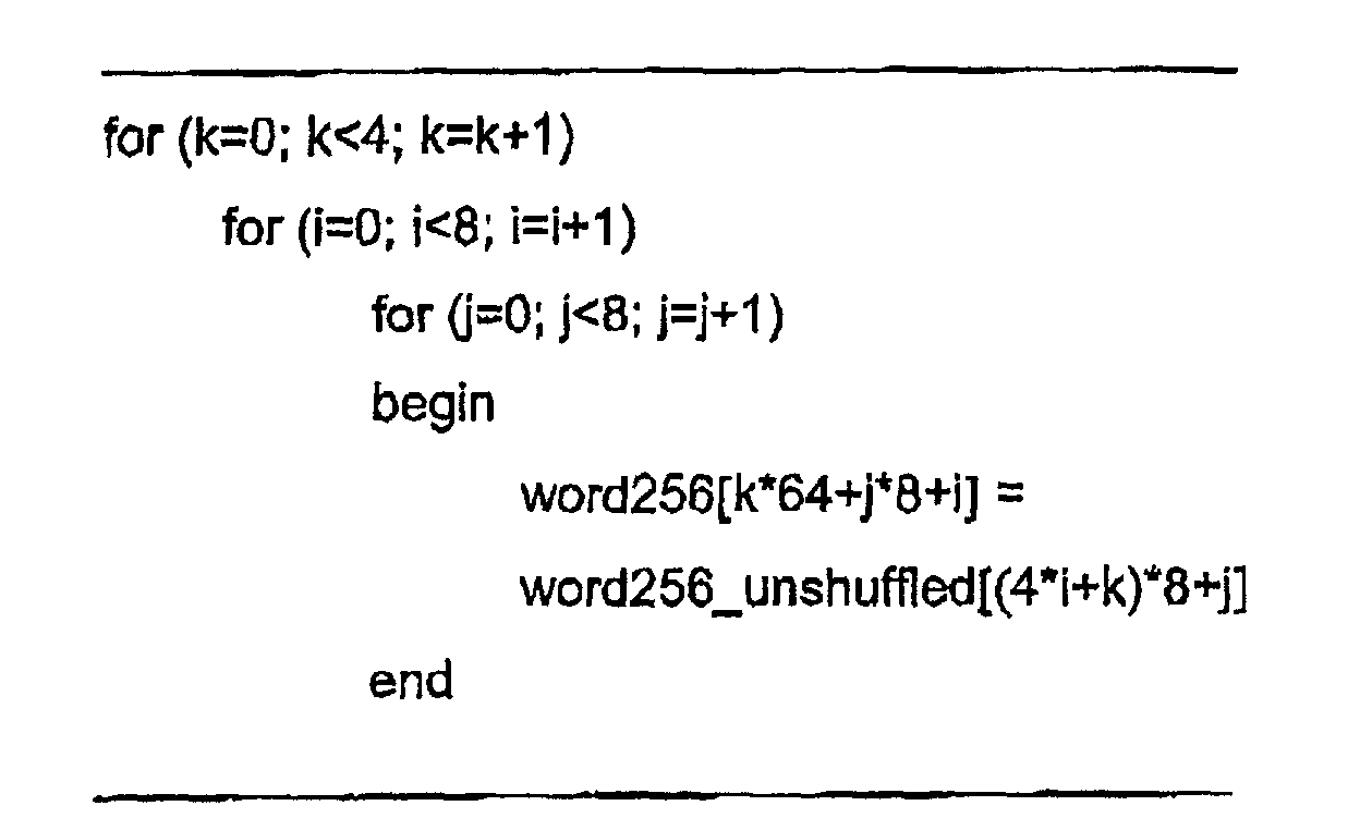
- Computerprozessor nach Anspruch 14, bei dem die Bits gemäß dem folgenden Algorithmus gemischt werdenwobei i, j und k ganzzahlige Indizies sind, word256 eine Matrix zur Speicherung von 256 Bits eines gemischten Wortes ist und word256_unshuffled eine Matrix zur Speicherung von 256 Bits eines nicht-gemischten Wortes ist.
- Computerprozessor nach Anspruch 5, der weiter erste und zweite Busse aufweist, wobei der erste Bus dazu bestimmt ist, Bits niedriger Ordnung eines Ausgabe-Wortes auszugeben und der zweite Bus dazu bestimmt ist, Bits hoher Ordnung eines Ausgabe-Wortes auszugeben.
- Computerprozessor nach Anspruch 16, bei dem als ein Ergebnis der Mischung der Bits die Leitungen der ersten und zweiten Busse in derselben Ebene des Prozessors ohne Kreuzung liegen können.
- Verfahren zur Erzeugung von Befehlen für einen Computerprozessor, dereinen Befehls-Cache (103) hat, der einen Eingabe-Bus und einen Ausgabe-Bus hat, wobei der Eingabe-Bus Bits eines Befehls zur Speicherung in dem Befehls-Cache empfängt,eine Verarbeitungseinheit (102) mit einem Befehlseingang hat, der mit dem Ausgabe-Bus zum Empfang der Bits des Befehls verbunden ist,
wobei das Verfahren die Schritte umfaßt, ein kompiliertes und gelinktes Objekt-Modul zu empfangen, das von einem Compiler und/oder einem Linker erzeugt ist,
weiter charakterisiert durch den SchrittBits in dem kompilierten und gelinkten Objekt-Modul zu mischen, um ein zweites Objekt-Modul zum Einschreiben in den Befehls-Speicher zu erzeugen, so daß die Bits des zweiten Objekt-Moduls auf dem Satz von parallelen Linien nacheinander in der Ordnung erscheinen, in der diese Bits in dem kompilierten und gelinkten Objekt-Modul erscheinen. - Verfahren nach Anspruch 18, bei dem eine Anzahl von Banken in dem Satz von Banken eine Potenz von 2 ist, wobei in dem Mischungs-Schritt jedes Bit des kompilierten und gelinkten Objekt-Moduls, das eine jeweilige erste Bit-Adresse in dem kompilierten und gelinkten Objekt-Modul hat, wobei auf eine jeweilige zweite Bit-Adresse in dem zweiten Objekt-Modul platziert wird, die jeweilige zweite Bit-Adresse eine logische Rotation der jeweiligen ersten Bit-Adresse um eine Anzahl mit dieser Potenz korrespondierender Bit-Plätze ist.
- Verfahren nach Anspruch 18 oder 19, das weiter den Schritt umfaßt, das zweite Objekt-Modul in einen Instruktions-Speicher zu schreiben.
- Verfahren nach Anspruch 18, 19 oder 20, bei dem der Befehls-Speicher einen Hauptspeicher und einen Cach-Speicher aufweist, wobei der Satz von Banken in dem Cach-Speicher enthalten ist.
- Ein Computerprogramm, das Programm-Code-Mittel zur Ausführung aller Verfahrensschritte eines der Ansprüche 18 bis 21 aufweist, wenn dieses Programm auf einem Computer abläuft.
- Ein Computerprogramm-Produkt, das auf einem Computer lesbaren Medium gespeicherte Programm-Code-Mittel zur Ausführung der Verfahrensschritte eines der Ansprüche 18 bis 21 aufweist, wenn dieses Programm-Produkt auf einem Computer abläuft.
- Ein auf einem Computerspeichermedium gespeicherter Bit-Strom, bei dem der Bit-Strom zumindest einen Teil eines Befehls zur Ausführung auf einem Computerprozessor beinhaltet,dadurch gekennzeichnet, daß der Teil eine Vielzahl von Bits beinhaltet, die sich in einer gemischten Ordnung befinden, wobei die gemischte Ordnung ein vereinfachtes Chip-Layout des Computerprozessors ermöglicht.der einen Befehls-Speicher (103) aufweist, der einen Eingabe-Bus und einen Ausgabe-Bus hat, wobei der Eingabe-Bus Bits eines Befehls zur Speicherung in dem Befehls-Cache empfängt,der eine Verarbeitungseinheit (102) mit einem Befehls-Eingang aufweist, der mit dem Ausgabe-Bus zum Empfang der Bits des Befehls gekoppelt ist,
- Bit-Strom nach Anspruch 24, wobei die Bits nach dem folgenden Algorithmus gemischt sind:wobei i, j und k ganzzahlige Indizies sind, word256 eine Matrix zur Speicherung von 256 Bits eines gemischten Wortes ist und word256_unshuffled eine Matrix zur Speicherung von 256 Bits eines nicht-gemischten Wortes ist,

- Bit-Strom nach Anspruch 24 oder 25, bei dem der Befehl 512 Bits hat.
- Bit-Strom nach Anspruch 24, bei dem das vereinfachte Layout der Gestalt ist, daß innerhalb eines Befehls-Caches des Computerprozessors alle Leitungen von allen Eingabe- und Ausgabe-Bussen innerhalb einer einzigen Ebene einer integrierten Schaltung liegen.
Applications Claiming Priority (5)
| Application Number | Priority Date | Filing Date | Title |
|---|---|---|---|
| US648333 | 1996-05-15 | ||
| US08/648,333 US6131152A (en) | 1996-05-15 | 1996-05-15 | Planar cache layout and instruction stream therefor |
| US08/649,732 US5862398A (en) | 1996-05-15 | 1996-05-15 | Compiler generating swizzled instructions usable in a simplified cache layout |
| US649732 | 1996-05-15 | ||
| PCT/IB1997/000552 WO1997043715A2 (en) | 1996-05-15 | 1997-05-14 | Processor with an instruction cache |
Publications (2)
| Publication Number | Publication Date |
|---|---|
| EP0846291A2 EP0846291A2 (de) | 1998-06-10 |
| EP0846291B1 true EP0846291B1 (de) | 2003-07-30 |
Family
ID=27095356
Family Applications (1)
| Application Number | Title | Priority Date | Filing Date |
|---|---|---|---|
| EP97918302A Expired - Lifetime EP0846291B1 (de) | 1996-05-15 | 1997-05-14 | Prozessor mit befehlscachespeicher |
Country Status (5)
| Country | Link |
|---|---|
| EP (1) | EP0846291B1 (de) |
| JP (1) | JP3706633B2 (de) |
| CN (1) | CN1145099C (de) |
| DE (1) | DE69723804T2 (de) |
| WO (1) | WO1997043715A2 (de) |
Families Citing this family (3)
| Publication number | Priority date | Publication date | Assignee | Title |
|---|---|---|---|---|
| WO2000070446A2 (en) * | 1999-05-13 | 2000-11-23 | Arc International U.S. Holdings Inc. | Method and apparatus for loose register encoding within a pipelined processor |
| GB0400660D0 (en) * | 2004-01-13 | 2004-02-11 | Koninkl Philips Electronics Nv | Method and related device for use in decoding executable code |
| US7296120B2 (en) * | 2004-11-18 | 2007-11-13 | International Business Machines Corporation | Mechanism that provides efficient multi-word load atomicity |
Family Cites Families (5)
| Publication number | Priority date | Publication date | Assignee | Title |
|---|---|---|---|---|
| US5179680A (en) * | 1987-04-20 | 1993-01-12 | Digital Equipment Corporation | Instruction storage and cache miss recovery in a high speed multiprocessing parallel processing apparatus |
| JP2810068B2 (ja) * | 1988-11-11 | 1998-10-15 | 株式会社日立製作所 | プロセッサシステム、コンピュータシステム及び命令処理方法 |
| WO1991004536A1 (en) * | 1989-09-20 | 1991-04-04 | Dolphin Server Technology A/S | Instruction cache architecture for parallel issuing of multiple instructions |
| AU5412594A (en) * | 1992-11-05 | 1994-05-24 | Commonwealth Of Australia, The | Data formatter |
| WO1994027216A1 (en) * | 1993-05-14 | 1994-11-24 | Massachusetts Institute Of Technology | Multiprocessor coupling system with integrated compile and run time scheduling for parallelism |
-
1997
- 1997-05-14 CN CNB971908508A patent/CN1145099C/zh not_active Expired - Fee Related
- 1997-05-14 EP EP97918302A patent/EP0846291B1/de not_active Expired - Lifetime
- 1997-05-14 DE DE69723804T patent/DE69723804T2/de not_active Expired - Lifetime
- 1997-05-14 JP JP54069597A patent/JP3706633B2/ja not_active Expired - Fee Related
- 1997-05-14 WO PCT/IB1997/000552 patent/WO1997043715A2/en not_active Ceased
Also Published As
| Publication number | Publication date |
|---|---|
| WO1997043715A2 (en) | 1997-11-20 |
| EP0846291A2 (de) | 1998-06-10 |
| DE69723804D1 (de) | 2003-09-04 |
| JP3706633B2 (ja) | 2005-10-12 |
| WO1997043715A3 (en) | 1998-01-22 |
| JPH11509663A (ja) | 1999-08-24 |
| CN1197519A (zh) | 1998-10-28 |
| DE69723804T2 (de) | 2004-05-27 |
| CN1145099C (zh) | 2004-04-07 |
Similar Documents
| Publication | Publication Date | Title |
|---|---|---|
| US5878267A (en) | Compressed instruction format for use in a VLIW processor and processor for processing such instructions | |
| US5826054A (en) | Compressed Instruction format for use in a VLIW processor | |
| US8583895B2 (en) | Compressed instruction format for use in a VLIW processor | |
| US6131152A (en) | Planar cache layout and instruction stream therefor | |
| US5930508A (en) | Method for storing and decoding instructions for a microprocessor having a plurality of function units | |
| US5819058A (en) | Instruction compression and decompression system and method for a processor | |
| KR100290325B1 (ko) | 긴명령워드를갖는처리기 | |
| US5410727A (en) | Input/output system for a massively parallel, single instruction, multiple data (SIMD) computer providing for the simultaneous transfer of data between a host computer input/output system and all SIMD memory devices | |
| US7953955B2 (en) | Methods and apparatus for automated generation of abbreviated instruction set and configurable processor architecture | |
| US6343356B1 (en) | Methods and apparatus for dynamic instruction controlled reconfiguration register file with extended precision | |
| US8069337B2 (en) | Methods and apparatus for dynamic instruction controlled reconfigurable register file | |
| US6925553B2 (en) | Staggering execution of a single packed data instruction using the same circuit | |
| US4502111A (en) | Token generator | |
| US5852741A (en) | VLIW processor which processes compressed instruction format | |
| SK93491A3 (en) | Digital computer system for elaborating of at lest two parallel instructions | |
| EP1365318A2 (de) | Microprozessor mit Matrixmodul zur Datenmanipulation | |
| US20030188128A1 (en) | Executing stack-based instructions within a data processing apparatus arranged to apply operations to data items stored in registers | |
| JPH06162227A (ja) | ベクトル並列計算機 | |
| US5862398A (en) | Compiler generating swizzled instructions usable in a simplified cache layout | |
| EP0843848B1 (de) | Vliw-prozessor zur verarbeitung eines komprimierten instruktionsformats | |
| US20070079305A1 (en) | Alignment of variable length program instructions within a data processing apparatus | |
| EP0846291B1 (de) | Prozessor mit befehlscachespeicher | |
| HK1034333B (en) | Processor utilizing template field instruction encoding | |
| HK1034333A1 (zh) | 利用規格字段指令編碼的處理器 | |
| JPH02236650A (ja) | スワツプデータバツフア装置 |
Legal Events
| Date | Code | Title | Description |
|---|---|---|---|
| PUAI | Public reference made under article 153(3) epc to a published international application that has entered the european phase |
Free format text: ORIGINAL CODE: 0009012 |
|
| AK | Designated contracting states |
Kind code of ref document: A2 Designated state(s): DE FR GB |
|
| RAP3 | Party data changed (applicant data changed or rights of an application transferred) |
Owner name: KONINKLIJKE PHILIPS ELECTRONICS N.V. |
|
| 17P | Request for examination filed |
Effective date: 19980722 |
|
| RAP1 | Party data changed (applicant data changed or rights of an application transferred) |
Owner name: TRIMEDIA TECHNOLOGIES, INC. |
|
| 17Q | First examination report despatched |
Effective date: 20010319 |
|
| GRAH | Despatch of communication of intention to grant a patent |
Free format text: ORIGINAL CODE: EPIDOS IGRA |
|
| GRAH | Despatch of communication of intention to grant a patent |
Free format text: ORIGINAL CODE: EPIDOS IGRA |
|
| GRAA | (expected) grant |
Free format text: ORIGINAL CODE: 0009210 |
|
| AK | Designated contracting states |
Designated state(s): DE FR GB |
|
| REG | Reference to a national code |
Ref country code: GB Ref legal event code: FG4D |
|
| REF | Corresponds to: |
Ref document number: 69723804 Country of ref document: DE Date of ref document: 20030904 Kind code of ref document: P |
|
| ET | Fr: translation filed | ||
| PLBE | No opposition filed within time limit |
Free format text: ORIGINAL CODE: 0009261 |
|
| STAA | Information on the status of an ep patent application or granted ep patent |
Free format text: STATUS: NO OPPOSITION FILED WITHIN TIME LIMIT |
|
| 26N | No opposition filed |
Effective date: 20040504 |
|
| REG | Reference to a national code |
Ref country code: GB Ref legal event code: 732E |
|
| REG | Reference to a national code |
Ref country code: GB Ref legal event code: 732E |
|
| REG | Reference to a national code |
Ref country code: FR Ref legal event code: TP |
|
| REG | Reference to a national code |
Ref country code: GB Ref legal event code: 732E Free format text: REGISTERED BETWEEN 20120301 AND 20120307 |
|
| REG | Reference to a national code |
Ref country code: DE Ref legal event code: R082 Ref document number: 69723804 Country of ref document: DE Representative=s name: MUELLER - HOFFMANN & PARTNER PATENTANWAELTE, DE |
|
| REG | Reference to a national code |
Ref country code: DE Ref legal event code: R082 Ref document number: 69723804 Country of ref document: DE Representative=s name: MUELLER - HOFFMANN & PARTNER PATENTANWAELTE, DE Effective date: 20120425 Ref country code: DE Ref legal event code: R081 Ref document number: 69723804 Country of ref document: DE Owner name: NYTELL SOFTWARE LLC, US Free format text: FORMER OWNER: NXP B.V., EINDHOVEN, NL Effective date: 20120425 |
|
| REG | Reference to a national code |
Ref country code: FR Ref legal event code: TP Owner name: NYTELL SOFTWARE LLC, US Effective date: 20120521 |
|
| PGFP | Annual fee paid to national office [announced via postgrant information from national office to epo] |
Ref country code: DE Payment date: 20120531 Year of fee payment: 16 |
|
| PGFP | Annual fee paid to national office [announced via postgrant information from national office to epo] |
Ref country code: GB Payment date: 20120426 Year of fee payment: 16 Ref country code: FR Payment date: 20120510 Year of fee payment: 16 |
|
| GBPC | Gb: european patent ceased through non-payment of renewal fee |
Effective date: 20130514 |
|
| PG25 | Lapsed in a contracting state [announced via postgrant information from national office to epo] |
Ref country code: DE Free format text: LAPSE BECAUSE OF NON-PAYMENT OF DUE FEES Effective date: 20131203 |
|
| REG | Reference to a national code |
Ref country code: DE Ref legal event code: R119 Ref document number: 69723804 Country of ref document: DE Effective date: 20131203 |
|
| REG | Reference to a national code |
Ref country code: FR Ref legal event code: ST Effective date: 20140131 |
|
| PG25 | Lapsed in a contracting state [announced via postgrant information from national office to epo] |
Ref country code: GB Free format text: LAPSE BECAUSE OF NON-PAYMENT OF DUE FEES Effective date: 20130514 |
|
| PG25 | Lapsed in a contracting state [announced via postgrant information from national office to epo] |
Ref country code: FR Free format text: LAPSE BECAUSE OF NON-PAYMENT OF DUE FEES Effective date: 20130531 |