EP0847048A1 - Elément à limitation d'ouverture et tête optique pourvue d'un tel élément - Google Patents
Elément à limitation d'ouverture et tête optique pourvue d'un tel élément Download PDFInfo
- Publication number
- EP0847048A1 EP0847048A1 EP97121181A EP97121181A EP0847048A1 EP 0847048 A1 EP0847048 A1 EP 0847048A1 EP 97121181 A EP97121181 A EP 97121181A EP 97121181 A EP97121181 A EP 97121181A EP 0847048 A1 EP0847048 A1 EP 0847048A1
- Authority
- EP
- European Patent Office
- Prior art keywords
- aperture
- limiting element
- transparent electrodes
- optical
- stripe
- Prior art date
- Legal status (The legal status is an assumption and is not a legal conclusion. Google has not performed a legal analysis and makes no representation as to the accuracy of the status listed.)
- Granted
Links
Images


Classifications
-
- G—PHYSICS
- G11—INFORMATION STORAGE
- G11B—INFORMATION STORAGE BASED ON RELATIVE MOVEMENT BETWEEN RECORD CARRIER AND TRANSDUCER
- G11B7/00—Recording or reproducing by optical means, e.g. recording using a thermal beam of optical radiation by modifying optical properties or the physical structure, reproducing using an optical beam at lower power by sensing optical properties; Record carriers therefor
- G11B7/12—Heads, e.g. forming of the optical beam spot or modulation of the optical beam
- G11B7/135—Means for guiding the beam from the source to the record carrier or from the record carrier to the detector
- G11B7/139—Numerical aperture control means
-
- G—PHYSICS
- G02—OPTICS
- G02F—OPTICAL DEVICES OR ARRANGEMENTS FOR THE CONTROL OF LIGHT BY MODIFICATION OF THE OPTICAL PROPERTIES OF THE MEDIA OF THE ELEMENTS INVOLVED THEREIN; NON-LINEAR OPTICS; FREQUENCY-CHANGING OF LIGHT; OPTICAL LOGIC ELEMENTS; OPTICAL ANALOGUE/DIGITAL CONVERTERS
- G02F1/00—Devices or arrangements for the control of the intensity, colour, phase, polarisation or direction of light arriving from an independent light source, e.g. switching, gating or modulating; Non-linear optics
- G02F1/01—Devices or arrangements for the control of the intensity, colour, phase, polarisation or direction of light arriving from an independent light source, e.g. switching, gating or modulating; Non-linear optics for the control of the intensity, phase, polarisation or colour
- G02F1/03—Devices or arrangements for the control of the intensity, colour, phase, polarisation or direction of light arriving from an independent light source, e.g. switching, gating or modulating; Non-linear optics for the control of the intensity, phase, polarisation or colour based on ceramics or electro-optical crystals, e.g. exhibiting Pockels effect or Kerr effect
- G02F1/0305—Constructional arrangements
- G02F1/0316—Electrodes
-
- G—PHYSICS
- G11—INFORMATION STORAGE
- G11B—INFORMATION STORAGE BASED ON RELATIVE MOVEMENT BETWEEN RECORD CARRIER AND TRANSDUCER
- G11B7/00—Recording or reproducing by optical means, e.g. recording using a thermal beam of optical radiation by modifying optical properties or the physical structure, reproducing using an optical beam at lower power by sensing optical properties; Record carriers therefor
- G11B7/12—Heads, e.g. forming of the optical beam spot or modulation of the optical beam
- G11B7/135—Means for guiding the beam from the source to the record carrier or from the record carrier to the detector
- G11B7/1365—Separate or integrated refractive elements, e.g. wave plates
- G11B7/1369—Active plates, e.g. liquid crystal panels or electrostrictive elements
-
- G—PHYSICS
- G11—INFORMATION STORAGE
- G11B—INFORMATION STORAGE BASED ON RELATIVE MOVEMENT BETWEEN RECORD CARRIER AND TRANSDUCER
- G11B7/00—Recording or reproducing by optical means, e.g. recording using a thermal beam of optical radiation by modifying optical properties or the physical structure, reproducing using an optical beam at lower power by sensing optical properties; Record carriers therefor
- G11B7/12—Heads, e.g. forming of the optical beam spot or modulation of the optical beam
- G11B7/135—Means for guiding the beam from the source to the record carrier or from the record carrier to the detector
- G11B7/1381—Non-lens elements for altering the properties of the beam, e.g. knife edges, slits, filters or stops
-
- G—PHYSICS
- G11—INFORMATION STORAGE
- G11B—INFORMATION STORAGE BASED ON RELATIVE MOVEMENT BETWEEN RECORD CARRIER AND TRANSDUCER
- G11B7/00—Recording or reproducing by optical means, e.g. recording using a thermal beam of optical radiation by modifying optical properties or the physical structure, reproducing using an optical beam at lower power by sensing optical properties; Record carriers therefor
- G11B2007/0003—Recording, reproducing or erasing systems characterised by the structure or type of the carrier
- G11B2007/0006—Recording, reproducing or erasing systems characterised by the structure or type of the carrier adapted for scanning different types of carrier, e.g. CD & DVD
-
- G—PHYSICS
- G11—INFORMATION STORAGE
- G11B—INFORMATION STORAGE BASED ON RELATIVE MOVEMENT BETWEEN RECORD CARRIER AND TRANSDUCER
- G11B7/00—Recording or reproducing by optical means, e.g. recording using a thermal beam of optical radiation by modifying optical properties or the physical structure, reproducing using an optical beam at lower power by sensing optical properties; Record carriers therefor
- G11B7/12—Heads, e.g. forming of the optical beam spot or modulation of the optical beam
- G11B7/135—Means for guiding the beam from the source to the record carrier or from the record carrier to the detector
- G11B7/1372—Lenses
- G11B2007/13727—Compound lenses, i.e. two or more lenses co-operating to perform a function, e.g. compound objective lens including a solid immersion lens, positive and negative lenses either bonded together or with adjustable spacing
Definitions
- the present invention relates to an aperture-limiting element and also an optical head utilizing the same, and more particularly to an aperture-limiting element which permits a single optical system to be compatible with a plurality of different optical recording media and also an optical head utilizing the same.
- CDs Compact Disks
- CD-ROMs Compact Disks for music reproduction
- CD-ROMs for data file read-only optical disk
- CDs Compact Disks
- DVDs Digital Video Disks
- These DVDs have the same size as the conventional CDs and CD-ROMs, while having large capacity of data recording in reduced-size and high-density pits.
- optical heads for reproducing the DVD the optical wavelength is made short as compared with that in the prior art, and the numerical aperture (NA) of an objective lens is made large thus reducing a converged beam spot so as to permit reading pits of the reduced size.
- NA numerical aperture
- optical heads for the DVDS use a laser with a wavelength of 635 to 650 nm and an objective lens with the NA of 0.6
- those for the conventional CDs and CD-ROMs use a laser with a wavelength of 785 nm and an objective lens with the NA of about 0.45.
- the substrate thickness is set to 0.6 mm.
- two substrates each with 0.6 mm thickness are bonded together to provide a total thickness of 1.2 mm, but the light is reflected by the interface between them, i.e., at a depth of 0.6 mm corresponding to the thickness of one of them.
- Objective lenses for the DVDs are designed in conformity to the substrate thickness of 0.6 mm.
- Fig. 1 shows a prior art example of system introduced in magazines (i.e., Nikkei Mechanical, No. 473, February 5, 1996, p. 16 and Nikkei Electronics, No. 654, January 29, 1996, pp. 15-16).
- a light beam from a light source 51 is transmitted through a collimating lens 52, a liquid crystal shutter 58 and a beam splitter 53 and converged by a DVD objective lens 56 to be incident on an optical disk 57.
- the return light beam is reflected by the beam splitter 53, transmitted through a collective lens 61 and a cylindrical lens 62, and received by a photo-detector 63 which detects a reproduced signal, a focus error signal and a tracking error signal.
- the liquid crystal shutter 58 provides NA limitation, that is, it limits the aperture of the objective lens to a small value of about 0.35 from 0.6.
- the liquid crystal shutter 58 is normally fully transparent. In its "on" state, however, the liquid crystal shutter 58 blocks light at a peripheral portion thereof, while leaving at a center portion thereof a circular transparent region. In this way, of the light collimated by the collimating lens, the light at the peripheral portion that causes the generation of the aberration is blocked, and only the light of the center portion is transmitted, so that the aberration is reduced, thus making it possible to reproduce a CD-ROM.
- the liquid crystal shutter 58 is held “off" to provide a fully transparent state with the NA being 0.6.
- the liquid crystal shutter 58 is held "on" to block light so that an NA value becomes about 0.35.
- Liquid crystals shown in Figs. 3A and 3B are generally called twisted nematic liquid crystals.
- the liquid crystal 66 is sandwiched between a first transparent electrode 65 and a second transparent electrode 67 in the light transmission direction.
- a first polarizer 64 and a second polarizer 68, respectively, are provided such that their polarization directions cross each other.
- the above prior art aperture-limiting element include at least two polarizers and two electrodes with the liquid crystal intervening therebetween. That is, the element requires a large number of components and tends to be increased in scale. This means that an optical head utilizing this element includes a large number of components and tends to be expensive.
- An object of the present invention is to overcome the problems existing in the prior art, and to provide an aperture-limiting element which can be constructed with a reduced number of components, and also an optical head employing the same element.
- an aperture-limiting element comprising: a plurality of stripe transparent electrodes spaced apart at a predetermined interval on an electro-optical crystal substrate; and a substantially circular non-electrode area lacking the stripe transparent electrodes at a center portion of the substrate.
- the aperture-limiting element may further includes a plurality of phase compensation films each provided between respective ones of the stripe transparent electrodes.
- an optical head having a light source, a collimating lens, an aperture-limiting element and an objective lens, the collimating lens, the aperture-limiting element and the objective lens being disposed in the mentioned order in the direction of progress of light emitted from the light source, and a photo-detecting system for detecting return light having been transmitted through the objective lens and reflected by an optical disk
- the aperture-limiting element comprising: a plurality of stripe transparent electrodes spaced apart at a predetermined interval on an electro-optical crystal substrate; and a substantially circular non-electrode area lacking the stripe transparent electrodes at a center portion of the substrate.
- stripe transparent electrodes The transparent electrodes in stripes provided at a predetermined interval on the electro-optical crystal substrate are hereinafter referred to as "stripe transparent electrodes".
- the refractive index of the substrate is changed in a region thereof where the stripe transparent electrodes are provided.
- This region alone thus functions as a phase diffraction grating, and incident light proceeds straight and is transmitted through only the central non-electrode region.
- the peripheral electrode region of the substrate functions merely as a transparent region as does the central non-electrode region.
- no voltage is applied to the stripe transparent electrodes.
- CD-ROM reproduction since the aperture should be limited, a voltage is applied.
- a light beam from a light source 1 is transmitted through a collimating lens 2, a beam splitter 3 and an aperture-limiting element 4 and then converged through an objective lens 6 for DVD before being incident on an optical disk 7.
- the return light beam is reflected by the beam splitter 3 and then transmitted through a collective lens 11 and a cylindrical lens 12 before being received by a photo-detector 13 which detects a reproduced signal, a focus error signal and a tracking error signal.
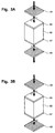
- Fig. 5A is a perspective view showing the aperture-limiting element 4.
- the aperture-limiting element 4 is constructed by arranging on one surface of an electro-optical crystal substrate 22 a plurality of parallel stripe transparent electrodes 20 and providing a substantially circular non-electrode area 23 having no transparent electrode 20 at a center portion of the substrate surface.
- a phase compensation film 21 is provided on the exposed substrate surface areas not occupied by the stripe transparent electrodes 20. This means that the phase compensation film 21 covers the entire non-electrode area 23.
- the phase compensation film 21 has a thickness less than the thickness of the electrode 20, so that it has an uneven light incidence surface formed by the provision of the stripes.
- the phase compensation film 21 is a dielectric film such as that of glass, and functions to cancel out the phase generated by the refractive index of the stripe transparent electrodes 20.
- the stripe transparent electrodes 20 are connected to a power supply for applying a voltage to them in CD-ROM reproduction.
- a grounded transparent electrode 19 is provided on the entire other surface of the electro-optical crystal substrate 22.
- the transparent electrodes 19 and 20 may be formed by using ITO, for instance.
- the electro-optical crystal substrate 22 may be formed by using LiNbO 3 , LiTaO 3 , KDP, etc.
- the aperture-limiting element 4 is disposed on the optical path with its uneven surface side facing opposite the objective lens 6.
- the uneven surface side may well face the objective lens 6.
- the stripe region In the state where the voltage is not being applied to the stripe transparent electrodes 20, the stripe region does not function as a diffraction grating, but functions as a transparent region.
- a voltage is applied to the Stripe transparent electrodes 20, a potential difference is generated between the stripe transparent electrodes 20 and the opposite side transparent electrode 19.
- the potential difference thus generated causes an electro-optical effect in the stripe region of the electro-optical crystal substrate 22 on which the stripe transparent electrodes 20 are provided.
- the electro-optical effect thus generated causes a change in the refractive index. Consequently, the stripe region functions as a phase type diffraction grating to change the optical path by diffracting the light coming straight and being incident. This region thus blocks the incident light in effect.
- the aperture-limiting element fulfills its role.
- the stripe transparent electrodes 20 In this case, as shown in Fig. 6A, the stripe region remains transparent, providing no aperture limitation. Thus, the entire objective lens with a high NA value of 0.6 is used for reproducing the DVD 7a.
- the stripe region functions as a diffraction grating. That is, light incident on the peripheral stripe region is diffracted, and light incident on only the central non-electrode region can proceed straight and be transmitted. This means that the aperture is reduced in effect, so that CD-ROM 7b having the thickness of 1.2 mm is illuminated and reproduced.
- the aperture-limiting element thus permits reproducing both DVDS and CD-ROMs with switching of the NA in effect by on-off switching of the applied voltage.
- the function of the aperture-limiting element can be realized by arranging thin film stripe electrodes on one surface of an electro-optical crystal substrate, and providing a non-electrode area at a center portion thereof, the number of components can be greatly reduced compared to the prior art construction. Since the number of components can be greatly reduced, it is possible to provide an optical head which is inexpensive compared to prior art optical heads.
- each phase compensation film is provided between respective adjacent stripe transparent electrodes, the phase generated due to the refractive index of the Stripe transparent electrodes themselves can be canceled out.
- Fig. 7 shows an aperture-limiting element in a different embodiment of the invention.
- the aperture-limiting element in this embodiment is obtained by covering the front and back side surfaces of the aperture-limiting element in the preceding embodiment with antireflection films 24. With this arrangement, transmittivity reduction due to reflection can be prevented.
- the antireflection film 24 may be a single-layer film or a multiple-layer film.
- Fig. 8 shows an aperture-limiting element in a further embodiment of the invention.
- the aperture-limiting element in this embodiment is obtained by excluding the back side transparent electrode 19 in the previous embodiment, and the stripe transparent electrodes 20 are adapted such that, in CD-ROM reproduction, voltage is applied to every other ones of them while the other ones are grounded. Again with this arrangement, the same functions and effects as obtainable with the aperture-limiting element shown in Figs. 5A and 5B can be obtained. Besides, since the back side transparent electrode 19 is dispensed with, the number of components can further be reduced.
- the advantage achieved with the construction according to the invention is that, with a voltage applied to the stripe transparent electrodes, the refractive index in this region of the electro-optical crystal substrate is changed, so that this region functions as a diffraction grating. Light thus can proceed straight and be transmitted through only the central non-electrode region.
- the aperture-limiting element thus permits reproducing both DVDs and CD-ROMs with the switching of the NA in effect by on-off switching of the applied voltage.
- the function of the aperture-limiting element can be realized by providing thin film stripe electrodes on one surface of an electro-optical crystal substrate except for a central non-electric area, the number of components can be greatly reduced compared to those required in the prior art construction.
- the phase compensation film which is provided on areas not occupied by the stripe transparent electrodes, can cancel out the phase due to the refractive index of the stripe transparent electrodes.
Landscapes
- Physics & Mathematics (AREA)
- Optics & Photonics (AREA)
- Chemical & Material Sciences (AREA)
- Crystallography & Structural Chemistry (AREA)
- Nonlinear Science (AREA)
- Engineering & Computer Science (AREA)
- Ceramic Engineering (AREA)
- General Physics & Mathematics (AREA)
- Optical Head (AREA)
Applications Claiming Priority (3)
| Application Number | Priority Date | Filing Date | Title |
|---|---|---|---|
| JP32676596 | 1996-12-06 | ||
| JP326765/96 | 1996-12-06 | ||
| JP8326765A JPH10172171A (ja) | 1996-12-06 | 1996-12-06 | 開口制限素子及びこれを利用した光へッド装置 |
Publications (2)
| Publication Number | Publication Date |
|---|---|
| EP0847048A1 true EP0847048A1 (fr) | 1998-06-10 |
| EP0847048B1 EP0847048B1 (fr) | 2004-03-10 |
Family
ID=18191450
Family Applications (1)
| Application Number | Title | Priority Date | Filing Date |
|---|---|---|---|
| EP97121181A Expired - Lifetime EP0847048B1 (fr) | 1996-12-06 | 1997-12-02 | Elément à limitation d'ouverture et tête optique pourvue d'un tel élément |
Country Status (4)
| Country | Link |
|---|---|
| US (1) | US6031809A (fr) |
| EP (1) | EP0847048B1 (fr) |
| JP (1) | JPH10172171A (fr) |
| DE (1) | DE69728019T2 (fr) |
Families Citing this family (6)
| Publication number | Priority date | Publication date | Assignee | Title |
|---|---|---|---|---|
| JP2002090784A (ja) * | 2000-09-04 | 2002-03-27 | Samsung Electro Mech Co Ltd | 光制御素子及びそれを用いた情報記録再生装置並びに情報再生装置 |
| JP2002222536A (ja) * | 2001-01-25 | 2002-08-09 | Sony Corp | 光スポット整形装置及び方法、光ピックアップ装置、並びに光ディスク装置 |
| JP4003161B2 (ja) * | 2001-11-19 | 2007-11-07 | ソニー株式会社 | 光ヘッド、記録再生装置、及び光結合効率可変素子 |
| US7826329B2 (en) * | 2005-10-04 | 2010-11-02 | International Business Machines Corporation | Multi-layered media aberration compensation apparatus, method, and system |
| US7969673B2 (en) * | 2008-11-11 | 2011-06-28 | Phokus Research Group, Llc | Night vision instrument focus device |
| US9470912B2 (en) * | 2014-01-17 | 2016-10-18 | Gooch And Housego Plc | Chemically reduced lithium compound-based Q-switch |
Citations (6)
| Publication number | Priority date | Publication date | Assignee | Title |
|---|---|---|---|---|
| EP0731457A2 (fr) * | 1995-03-04 | 1996-09-11 | Lg Electronics Inc. | Appareil de lecture optique apte à lire des données sur n'importe quelle genre de disque |
| EP0745980A1 (fr) * | 1991-11-20 | 1996-12-04 | Sony Corporation | Dispositif de reproduction optique |
| EP0745977A1 (fr) * | 1995-05-24 | 1996-12-04 | Nec Corporation | Dispositif de tête optique |
| EP0747894A2 (fr) * | 1995-06-05 | 1996-12-11 | Nec Corporation | Dispositif de tête optique avec un grande tolérance à inclinaison |
| EP0762398A1 (fr) * | 1995-08-31 | 1997-03-12 | SANYO ELECTRIC Co., Ltd. | Appareil d'enregistrement/de reproduction pour disque optique pour l'enregistrement/la reproduction d'information sur disques optiques de types différents |
| WO1997031371A1 (fr) * | 1996-02-23 | 1997-08-28 | Toyo Communication Equipment Co., Ltd. | Excitation optique et element optique correspondant |
Family Cites Families (19)
| Publication number | Priority date | Publication date | Assignee | Title |
|---|---|---|---|---|
| US3787111A (en) * | 1973-04-16 | 1974-01-22 | Bell Telephone Labor Inc | Electrooptic grating for scanning a beam of light |
| JPH02287226A (ja) * | 1989-04-28 | 1990-11-27 | Anritsu Corp | 可変スリット装置 |
| US5093747A (en) * | 1991-02-28 | 1992-03-03 | Raytheon Company | Method for providing beam steering in a subaperture-addressed optical beam steerer |
| JPH05120720A (ja) * | 1991-10-28 | 1993-05-18 | Toshiba Corp | 情報記録・再生装置 |
| US5281797A (en) * | 1991-12-26 | 1994-01-25 | Hitachi, Ltd. | Short wavelength optical disk head having a changeable aperture |
| JP3292314B2 (ja) * | 1992-09-11 | 2002-06-17 | キヤノン株式会社 | 光学的検出装置 |
| JPH06110092A (ja) * | 1992-09-28 | 1994-04-22 | Nippon Telegr & Teleph Corp <Ntt> | 電気光学素子 |
| JPH06180851A (ja) * | 1992-12-11 | 1994-06-28 | Hitachi Maxell Ltd | 光ヘッド |
| JPH08212611A (ja) * | 1995-02-01 | 1996-08-20 | Asahi Optical Co Ltd | 波面収差補正装置および光情報記録再生装置 |
| JPH08321065A (ja) * | 1995-05-23 | 1996-12-03 | Hitachi Ltd | 光ディスク装置 |
| JP3476989B2 (ja) * | 1995-08-04 | 2003-12-10 | パイオニア株式会社 | 光ピックアップ |
| CN1158477A (zh) * | 1995-12-30 | 1997-09-03 | Lg电子株式会社 | 用于不同光盘的光学拾取装置 |
| US5798994A (en) * | 1996-01-16 | 1998-08-25 | Kamatani; Yasuo | Multi-layered optical disk reading method using liquid crystal diffraction device |
| JP3624561B2 (ja) * | 1996-03-12 | 2005-03-02 | 旭硝子株式会社 | 光変調素子及び光ヘッド装置 |
| JP3986580B2 (ja) * | 1996-04-04 | 2007-10-03 | 旭硝子株式会社 | 光変調素子及び光ヘッド装置 |
| JP3885251B2 (ja) * | 1996-06-10 | 2007-02-21 | 旭硝子株式会社 | 光学異方性回折格子、その駆動方法及びそれを用いた光ヘッド装置 |
| JPH1040570A (ja) * | 1996-07-22 | 1998-02-13 | Matsushita Electric Ind Co Ltd | 光量変調素子及び光ピックアップ装置 |
| JPH1064097A (ja) * | 1996-08-21 | 1998-03-06 | Minebea Co Ltd | 光ピックアップ装置 |
| JP3504082B2 (ja) * | 1996-09-03 | 2004-03-08 | パイオニア株式会社 | 収差補正光学装置及び記録媒体再生装置 |
-
1996
- 1996-12-06 JP JP8326765A patent/JPH10172171A/ja active Pending
-
1997
- 1997-12-02 EP EP97121181A patent/EP0847048B1/fr not_active Expired - Lifetime
- 1997-12-02 DE DE69728019T patent/DE69728019T2/de not_active Expired - Fee Related
- 1997-12-05 US US08/986,181 patent/US6031809A/en not_active Expired - Fee Related
Patent Citations (7)
| Publication number | Priority date | Publication date | Assignee | Title |
|---|---|---|---|---|
| EP0745980A1 (fr) * | 1991-11-20 | 1996-12-04 | Sony Corporation | Dispositif de reproduction optique |
| EP0731457A2 (fr) * | 1995-03-04 | 1996-09-11 | Lg Electronics Inc. | Appareil de lecture optique apte à lire des données sur n'importe quelle genre de disque |
| EP0745977A1 (fr) * | 1995-05-24 | 1996-12-04 | Nec Corporation | Dispositif de tête optique |
| EP0747894A2 (fr) * | 1995-06-05 | 1996-12-11 | Nec Corporation | Dispositif de tête optique avec un grande tolérance à inclinaison |
| EP0762398A1 (fr) * | 1995-08-31 | 1997-03-12 | SANYO ELECTRIC Co., Ltd. | Appareil d'enregistrement/de reproduction pour disque optique pour l'enregistrement/la reproduction d'information sur disques optiques de types différents |
| WO1997031371A1 (fr) * | 1996-02-23 | 1997-08-28 | Toyo Communication Equipment Co., Ltd. | Excitation optique et element optique correspondant |
| EP0823705A1 (fr) * | 1996-02-23 | 1998-02-11 | Toyo Communication Equipment Co. Ltd. | Excitation optique et element optique correspondant |
Also Published As
| Publication number | Publication date |
|---|---|
| DE69728019D1 (de) | 2004-04-15 |
| JPH10172171A (ja) | 1998-06-26 |
| EP0847048B1 (fr) | 2004-03-10 |
| US6031809A (en) | 2000-02-29 |
| DE69728019T2 (de) | 2004-07-22 |
Similar Documents
| Publication | Publication Date | Title |
|---|---|---|
| US6819646B1 (en) | Optical pickup, optical information recording/reproducing apparatus using the same, and phase variable wave plate used in the pickup and the apparatus | |
| US6618343B1 (en) | Optical information processor and optical element | |
| JP3067665B2 (ja) | 二種ディスク兼用光ピックアップ装置 | |
| JPH09198702A (ja) | 光ピックアップ装置 | |
| US20010033541A1 (en) | Aberration compensating apparatus and method | |
| EP1158335B1 (fr) | Dispositif de correction d'aberration, dispositif de lecture optique et dispositif d'enregistrement/reproduction | |
| EP1560209B1 (fr) | Element optique a cristaux liquides et dispositif optique | |
| EP0847048B1 (fr) | Elément à limitation d'ouverture et tête optique pourvue d'un tel élément | |
| KR100200873B1 (ko) | 광 픽업 장치 | |
| JP3861270B2 (ja) | 光ピックアップ及びそれに用いる光学素子 | |
| JP3624561B2 (ja) | 光変調素子及び光ヘッド装置 | |
| KR100200857B1 (ko) | 광픽업장치 | |
| JP2001176114A (ja) | ピックアップ装置及び情報記録再生装置 | |
| JP4695739B2 (ja) | 光学素子ならびにこれを用いた光ヘッドおよび光記録再生装置 | |
| JPH09161307A (ja) | 光学ヘッドおよび光学式情報再生装置 | |
| US6160783A (en) | Optical pick-up device | |
| JP4082085B2 (ja) | 光ヘッド装置 | |
| JP2718247B2 (ja) | 光学式ヘッド装置 | |
| JP4085527B2 (ja) | 光ヘッド装置 | |
| KR0176898B1 (ko) | 씨디/디브이디 겸용 광픽업장치 | |
| JPH1139704A (ja) | 光情報読み取り及び記録装置 | |
| JPH0254434A (ja) | 光学ヘッド | |
| KR100421354B1 (ko) | 광픽업장치 | |
| JP2003173564A (ja) | 光ヘッド装置 | |
| JPWO1999013464A1 (ja) | 光学装置 |
Legal Events
| Date | Code | Title | Description |
|---|---|---|---|
| PUAI | Public reference made under article 153(3) epc to a published international application that has entered the european phase |
Free format text: ORIGINAL CODE: 0009012 |
|
| AK | Designated contracting states |
Kind code of ref document: A1 Designated state(s): DE FR GB NL |
|
| AX | Request for extension of the european patent |
Free format text: AL;LT;LV;MK;RO;SI |
|
| 17P | Request for examination filed |
Effective date: 19980618 |
|
| AKX | Designation fees paid |
Free format text: DE FR GB NL |
|
| RBV | Designated contracting states (corrected) |
Designated state(s): DE FR GB NL |
|
| REG | Reference to a national code |
Ref country code: GB Ref legal event code: FG4D |
|
| GRAH | Despatch of communication of intention to grant a patent |
Free format text: ORIGINAL CODE: EPIDOS IGRA |
|
| GRAS | Grant fee paid |
Free format text: ORIGINAL CODE: EPIDOSNIGR3 |
|
| GRAA | (expected) grant |
Free format text: ORIGINAL CODE: 0009210 |
|
| AK | Designated contracting states |
Kind code of ref document: B1 Designated state(s): DE FR GB NL |
|
| REF | Corresponds to: |
Ref document number: 69728019 Country of ref document: DE Date of ref document: 20040415 Kind code of ref document: P |
|
| ET | Fr: translation filed | ||
| PLBE | No opposition filed within time limit |
Free format text: ORIGINAL CODE: 0009261 |
|
| STAA | Information on the status of an ep patent application or granted ep patent |
Free format text: STATUS: NO OPPOSITION FILED WITHIN TIME LIMIT |
|
| 26N | No opposition filed |
Effective date: 20041213 |
|
| PGFP | Annual fee paid to national office [announced via postgrant information from national office to epo] |
Ref country code: NL Payment date: 20081215 Year of fee payment: 12 |
|
| PGFP | Annual fee paid to national office [announced via postgrant information from national office to epo] |
Ref country code: FR Payment date: 20081212 Year of fee payment: 12 |
|
| PGFP | Annual fee paid to national office [announced via postgrant information from national office to epo] |
Ref country code: DE Payment date: 20081127 Year of fee payment: 12 |
|
| PGFP | Annual fee paid to national office [announced via postgrant information from national office to epo] |
Ref country code: GB Payment date: 20081126 Year of fee payment: 12 |
|
| REG | Reference to a national code |
Ref country code: NL Ref legal event code: V1 Effective date: 20100701 |
|
| GBPC | Gb: european patent ceased through non-payment of renewal fee |
Effective date: 20091202 |
|
| REG | Reference to a national code |
Ref country code: FR Ref legal event code: ST Effective date: 20100831 |
|
| PG25 | Lapsed in a contracting state [announced via postgrant information from national office to epo] |
Ref country code: NL Free format text: LAPSE BECAUSE OF NON-PAYMENT OF DUE FEES Effective date: 20100701 Ref country code: FR Free format text: LAPSE BECAUSE OF NON-PAYMENT OF DUE FEES Effective date: 20091231 |
|
| PG25 | Lapsed in a contracting state [announced via postgrant information from national office to epo] |
Ref country code: DE Free format text: LAPSE BECAUSE OF NON-PAYMENT OF DUE FEES Effective date: 20100701 |
|
| PG25 | Lapsed in a contracting state [announced via postgrant information from national office to epo] |
Ref country code: GB Free format text: LAPSE BECAUSE OF NON-PAYMENT OF DUE FEES Effective date: 20091202 |