EP0847075A2 - Source de positrons - Google Patents
Source de positrons Download PDFInfo
- Publication number
- EP0847075A2 EP0847075A2 EP97120440A EP97120440A EP0847075A2 EP 0847075 A2 EP0847075 A2 EP 0847075A2 EP 97120440 A EP97120440 A EP 97120440A EP 97120440 A EP97120440 A EP 97120440A EP 0847075 A2 EP0847075 A2 EP 0847075A2
- Authority
- EP
- European Patent Office
- Prior art keywords
- positron
- source
- electron
- emitter
- moderator
- Prior art date
- Legal status (The legal status is an assumption and is not a legal conclusion. Google has not performed a legal analysis and makes no representation as to the accuracy of the status listed.)
- Granted
Links
Images

Classifications
-
- H—ELECTRICITY
- H01—ELECTRIC ELEMENTS
- H01J—ELECTRIC DISCHARGE TUBES OR DISCHARGE LAMPS
- H01J37/00—Discharge tubes with provision for introducing objects or material to be exposed to the discharge, e.g. for the purpose of examination or processing thereof
- H01J37/26—Electron or ion microscopes; Electron or ion diffraction tubes
-
- H—ELECTRICITY
- H01—ELECTRIC ELEMENTS
- H01J—ELECTRIC DISCHARGE TUBES OR DISCHARGE LAMPS
- H01J2237/00—Discharge tubes exposing object to beam, e.g. for analysis treatment, etching, imaging
- H01J2237/06—Sources
- H01J2237/063—Electron sources
- H01J2237/06391—Positron sources
Definitions
- EP-B1 0 205 092 describes a scanning electron microscope which can be used to examine the sample either with electrons or with positrons and for this purpose the sample can optionally be irradiated with electrons or positrons.
- the positron beam and the electron beam are superimposed on one another by a deflecting magnet and subsequently guided along the optical axis of the magnetic lenses of the scanning microscope.
- the radioactive nuclide 22 Na which is largely e + active, is used as the positron source. In the beam direction, the radioactive nuclide is preceded by an aluminum foil, through which the positrons emitted by the nuclide are decelerated to thermal energy with an energy width of one electron volt.
- This source has a relatively large extension and therefore the phase space of the positrons is considerably larger than the phase space of the electrons.
- the yield of this type of moderation of the positrons is very low, since only the positrons diffused through the complete aluminum foil emerge again on the opposite side of the aluminum foil. Because of this low yield, the intensity of the positron source is very weak and therefore long measurement times are required for measurements of the electron / positron recombination in the sample.
- a further weakening of the positron beam occurs within the imaging optics of the electron microscope, in that a large part of the positrons in the area of the imaging optics is absorbed by the tube of the electron microscope.
- the aim of the present invention is a small intensive Positron source with a small energy bandwidth, which for one Use in an electron microscope is suitable. That goal is according to the invention by a positron source with the Features of claim 1 solved. Advantageous configurations the invention result from the features of the dependent Expectations.
- the positron source according to the invention contains a positron emitting nuclide of high specific activity as Positron emitter and one upstream of the emitter Reflection moderator.
- the reflection moderator is considered a thin one Sheet from a material with negative work function for the Positrons formed and has a hole with one emitter-side diameter of less than 0.4 mm, preferably 0.2 mm or 0.1 mm.
- the positron emitter is behind the hole of the reflection moderator.
- the hole of the Reflection moderator is preferably cylindrical or still better conical with one towards the positron emitter decreasing hole diameter.
- the positron emitter By arranging the positron emitter behind the hole of the reflection moderator, a large part of the positrons emitted hit the moderator material within the hole.
- the positrons are thermalized in the moderator material and then released from the moderator material with the exit energy. Since the positrons do not have to diffuse through the moderator for this purpose, but rather can remain in the area of the hole on the surface of the hole, the efficiency of the energy conversion in such a reflection moderator is considerably higher than in the case of a transmission moderator.
- this positron source has a yield of approximately 5 ⁇ 10 -4 behind the moderator.
- a further advantage of the reflection moderator compared to a transmission moderator results from the trimming of the positron-emitting surface, because the positrons emitted from the area regions of the positron emitter lying laterally outside the hole through the reflection moderator are caught by the moderator material. This results in the small lateral dimensions of the positron source; the small hole of the reflection moderator results in an almost punctiform positron source, the effective area of which corresponds to the hole diameter.
- the positron beam emerging from the reflection moderator can be imaged and focused comparably well by means of the magnetic lenses customary in electron microscopes, like an electron beam emitted from a hot cathode.
- the specific activity of the positron emitting material should be greater than 10 10 Bequerel (Bq) per gram, preferably greater than 10 14 Bq per gram.
- a positron source with such a high specific activity can be realized, for example, by evaporating a carrier-free positron-emitting nuclide, for example 22 Na, onto a non-radioactive carrier. By vapor deposition through a small aperture with an opening diameter of approximately 0.06 to 0.3 mm, it can be achieved that the area diameter of the area emitting the positrons also has an area diameter of less than 0.4 mm.
- the reflection moderator Material with negative work function for positrons in Consideration for example tungsten, copper, gold, nickel, Aluminum or solid noble gases.
- Tungsten Preferably used as a moderator material Tungsten used.
- the negative work function at Tungsten is 2.6 electron volts and the energy blur 75 milli-electron volts.
- the positron beam points a corresponding one immediately behind the moderator low energy blur.
- the hole through the reflection moderator is preferably conical with a smaller diameter on the side of the positron emitter than on the side facing away from the emitting emitter. Due to this conical design of the hole, an electrostatic Extraction field for extracting the positrons better in the Penetration hole of the reflection moderator, reducing the yield the source is increased.
- An adjustment unit is preferably provided, through which the Carrier on which the radioactive material is applied, relative to the reflection moderator in three perpendicular to each other Spatial directions is adjustable. With this adjustment unit the area emitting the positrons for optimal yield positioned immediately behind the moderator’s hole will.
- a further adjustment device is provided, either by the reflection moderator or the entire unit consisting of reflection moderator plus the adjustment unit for the wearer of the radioactive material in three mutually perpendicular spatial directions relative to the components of the downstream Imaging optics is adjustable. This allows the Positron source optimal to the beam axis of the imaging optics adjust.
- the positron source according to the invention preferably takes place Application in an electron microscope, in which over a Magnetic prism emitted by an electron source Electron beam and that emitted by the positron source Positron beam to be superimposed on each other.
- Such one Magnetic prism can have imaging properties and then serve both the positron source and the Electron source in the same cross-over level of the downstream Imaging optics.
- Such one Electron / positron microscope is then between electron operation and positron mode switchable by either the Electron beam and / or the positron beam in the Imaging beam path is coupled.
- both on the side of the electron source and also on the side of the positron source in front of the respective one Another magnetic lens enters the magnetic prism provided by which the positron beam and the electron beam be focused in the image plane of the magnetic prism.
- the air coils which are usually used for beam adjustment between the electron source and the condenser of the imaging optics, or as a stigmator between the condenser and the objective lens or as an electrostatic deflection unit for scanning one Sample are provided in a scanning electron microscope. At a scanning electron microscope with a deflection system for However, scanning the sample is preferred during positron operation the scanning unit is always set to the same, fixed default Position set and the object detail of interest via an adjustment unit of the sample holder brought preset position.
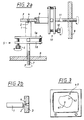
- FIG. 2a shows two adjustment devices.
- the carrier (1) for the radioactive material (2) is on one in a manner not shown electrically isolated usual Mirror bracket (5) added, and the mirror bracket (5) by means of a linear guide (7) relative to a device-fixed Carrier (8) adjustable.
- the linear guide (7) can simply as one with an internal thread in the device-fixed frame (8) Threaded spindle to be formed. By turning this threaded spindle (7) there is a linear displacement of the mirror holder (5) in the axial direction of the threaded spindle.
- the threaded spindle (11) is linearly displaced Mirror holder (10) parallel to the axis of the second threaded spindle (11) and by adjusting the two adjusting screws of the Mirror holder (10), of which in turn only in Figure 2a a single set screw (12) is shown, one takes place Adjustment of the reflection moderator (3) in the two to the axis the threaded spindle (11) vertical spatial directions.
- the positron source according to the invention is shown in FIG Combined with a scanning electron microscope.
- the positron source After leaving the moderator (3) the positron source the positrons by means of a suction electrode (21) opposite the moderator has a negative potential, sucked off and by means of an accelerating electrode (22) accelerates the desired target energy.
- the positron emitter (2) and the moderator are on positive high voltage.
- a double deflection system realized by air coils (23), a subsequent condenser lens (43), another simple deflection system (48) and a further deflection system (48) subsequent magnetic prism (20) is the positron beam deflected by 90 ° and at the same time into the input source plane (24) of the following imaging optics.
- the distraction system (48) is used for fine adjustment of the positron beam, while the double deflection system (23) for rough adjustment of the positron beam.
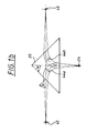
- the beam guidance of both the positron beam and the Electron beam in the area of the prism (20) is in the figure 1b.
- Both the condenser lens on the electron side (29) and the positron-side condenser lens (43) are like this excited that the crossover of the electron source into one Input source plane (46) and the crossover of the positron source into the other input source plane (45) of the magnetic prism (20) is mapped.
- the magnetic prism (20) then forms both Input source levels (45, 46) in the same output source level with a magnification of approx. 0.5, which corresponds to the input source level (24) of the following electron optical Imaging system coincides.
- the further simple Deflection system (48) for the adjustment of the positron beam is provided.
- Figure 1a has a conventional Structure and contains one of the input source level (24) downstream double deflection system (30) for beam adjustment, a two-stage condenser with magnetic lenses (31, 32), arranged on the outlet side of the condenser (31, 32) Stigmator coils and a lens (34) for focusing the Particle beam onto an object (37) on an object holder (38).
- the condenser lenses (31, 32) and the objective lens (34) are strong magnetic lenses and therefore have pole shoes magnetic soft iron.
- the coils of the for adjustment serving double deflection system (30) and the coil (33) for the Stigmators are designed as air coils.
- the A double deflection system is also integrated in the objective (34) (35, 36), through which the object (37) in a conventional manner can be scanned by means of the electron beam.
- the imaging properties of the Scanning electron microscope with the invention Positron source for positrons and electrons almost identical.
- Electron positron microscope usually takes place in such a way that first the object (37) by means of the electron beam scanned and the image of secondary electrons or backscattered electrons is observed.
- object (37) by means of the electron beam scanned and the image of secondary electrons or backscattered electrons is observed.
- Object details examined in more detail using the positron beam Regardless of the position within the electron image the relevant object detail is located, the Positron beam always focused on the same point, i.e. the double deflection system (35, 36) always so excited that a spatially fixed positron probe is realized in the form of the focused positron beam. Instead of the positron beam on the object detail of interest rather align the object detail of interest in brought the focus of the positron beam.
- the drive control of the sample holder (8) then moves the Sample holder (38) such that the marked object detail (42) into the stored position of the positron probe (41) brought.
- the magnetic prism (20) realized as a "three-sided" prism.
- other magnetic prisms are used that at the same time the condition of beam merging and Fulfill focus, for example in the form of a four-sided prism that maps four source planes one inside the other; the prism side opposite the exit side remains then unused.
Landscapes
- Chemical & Material Sciences (AREA)
- Analytical Chemistry (AREA)
- Analysing Materials By The Use Of Radiation (AREA)
- Particle Accelerators (AREA)
Applications Claiming Priority (2)
| Application Number | Priority Date | Filing Date | Title |
|---|---|---|---|
| DE19650694A DE19650694A1 (de) | 1996-12-06 | 1996-12-06 | Positronenquelle |
| DE19650694 | 1996-12-06 |
Publications (3)
| Publication Number | Publication Date |
|---|---|
| EP0847075A2 true EP0847075A2 (fr) | 1998-06-10 |
| EP0847075A3 EP0847075A3 (fr) | 2001-01-03 |
| EP0847075B1 EP0847075B1 (fr) | 2004-01-02 |
Family
ID=7813863
Family Applications (1)
| Application Number | Title | Priority Date | Filing Date |
|---|---|---|---|
| EP97120440A Expired - Lifetime EP0847075B1 (fr) | 1996-12-06 | 1997-11-21 | Source de positrons |
Country Status (3)
| Country | Link |
|---|---|
| US (1) | US6043489A (fr) |
| EP (1) | EP0847075B1 (fr) |
| DE (2) | DE19650694A1 (fr) |
Families Citing this family (6)
| Publication number | Priority date | Publication date | Assignee | Title |
|---|---|---|---|---|
| GB2374723B (en) * | 2001-04-20 | 2005-04-20 | Leo Electron Microscopy Ltd | Scanning electron microscope |
| US7041508B2 (en) * | 2002-02-06 | 2006-05-09 | Alerttechsystems, Llc | Positron annihilation monitor and method for detecting hazardous materials |
| JP2004340652A (ja) * | 2003-05-14 | 2004-12-02 | Hitachi Ltd | 欠陥検査装置および陽電子線応用装置 |
| US7420166B2 (en) * | 2004-07-14 | 2008-09-02 | The University Of Hong Kong | Real-time S-parameter imager |
| RU2530735C1 (ru) * | 2013-05-29 | 2014-10-10 | Федеральное государственное бюджетное образовательное учреждение высшего профессионального образования "Национальный исследовательский Томский политехнический университет" | Способ генерации ускоренных позитронов |
| US20150123003A1 (en) * | 2013-11-06 | 2015-05-07 | University Of Kentucky Research Foundation | High resolution absorption imaging using annihilation radiation from an external positron source |
Family Cites Families (1)
| Publication number | Priority date | Publication date | Assignee | Title |
|---|---|---|---|---|
| EP0205092B1 (fr) * | 1985-06-07 | 1992-09-02 | Hitachi, Ltd. | Méthode et dispositif pour analyser l'extinction de la position et microscope électronique ayant ledit appareil |
-
1996
- 1996-12-06 DE DE19650694A patent/DE19650694A1/de not_active Withdrawn
-
1997
- 1997-11-21 DE DE59711168T patent/DE59711168D1/de not_active Expired - Lifetime
- 1997-11-21 EP EP97120440A patent/EP0847075B1/fr not_active Expired - Lifetime
- 1997-12-05 US US08/985,397 patent/US6043489A/en not_active Expired - Lifetime
Also Published As
| Publication number | Publication date |
|---|---|
| DE19650694A1 (de) | 1998-06-10 |
| US6043489A (en) | 2000-03-28 |
| EP0847075B1 (fr) | 2004-01-02 |
| EP0847075A3 (fr) | 2001-01-03 |
| DE59711168D1 (de) | 2004-02-05 |
Similar Documents
| Publication | Publication Date | Title |
|---|---|---|
| EP1439565B1 (fr) | Appareil à faisceau électronique, et dispositif détecteur | |
| EP0893816B1 (fr) | Appareil à faisceau corpusculaire | |
| DE112014002951T5 (de) | Rasterelektronenmikroskop | |
| EP1835523A2 (fr) | Microscope à électrons à contraste de phase | |
| DE69920182T2 (de) | Korpuskularstrahloptisches gerät mit auger-elektronendetektion | |
| DE69501144T2 (de) | Teilchenoptisches gerät mit einem sekondärelektronen detektor | |
| DE2151167B2 (de) | Elektronenstrahl Mikroanalysator mit Auger Elektronen Nachweis | |
| DE102023106030A1 (de) | Elektronenstrahlmikroskop | |
| EP0911860B1 (fr) | Appareil à faisceau de particules chargées avec filtre en énergie | |
| DE102021112503B4 (de) | Teilchenstrahlvorrichtung mit einer Ablenkeinheit | |
| EP0847075B1 (fr) | Source de positrons | |
| EP1347490A2 (fr) | Accessoire de diaphragme pour microscope électronique à balayage | |
| DE3011625C2 (fr) | ||
| DE4041297A1 (de) | Verfahren und vorrichtung zum waehlen der aufloesung eines ladungsteilchenstrahl-analysators | |
| EP1087420B1 (fr) | Dispositif d'optique corpusculaire pour l'illumination et l'imagerie comprenant une lentille condenseur-objectif à champ unique et procédé de son utilisation | |
| DE102017208005B3 (de) | Teilchenquelle zur Erzeugung eines Teilchenstrahls und teilchenoptische Vorrichtung | |
| EP1774560B9 (fr) | Appareil a faisceau electronique | |
| DE102023131607B4 (de) | Verfahren zum Betreiben einer Teilchenstrahlvorrichtung, Computerprogrammprodukt und Teilchenstrahlvorrichtung zum Ausführen des Verfahrens | |
| DE2043749C3 (de) | Raster-Korpuskularstrahlmikroskop | |
| DE19650680B4 (de) | Elektronenmikroskop mit Positronenzusatz | |
| DE1764166C3 (de) | Ionen Elektronen Bildwandler | |
| DE1648980C3 (de) | Vorrichtung zur Röntgenspektrometrie | |
| DE102023131592A1 (de) | Verfahren zum Betrieb eines Teilchenstrahlgeräts, Computerprogrammprodukt sowie Teilchenstrahlgerät zur Durchführung des Verfahrens | |
| DE102024004580A1 (de) | Elektronenstrahlmikroskop | |
| DE2711536A1 (de) | Durchstrahlungs-raster-korpuskularstrahlmikroskop |
Legal Events
| Date | Code | Title | Description |
|---|---|---|---|
| PUAI | Public reference made under article 153(3) epc to a published international application that has entered the european phase |
Free format text: ORIGINAL CODE: 0009012 |
|
| AK | Designated contracting states |
Kind code of ref document: A2 Designated state(s): DE GB NL |
|
| AX | Request for extension of the european patent |
Free format text: AL;LT;LV;MK;RO;SI |
|
| PUAL | Search report despatched |
Free format text: ORIGINAL CODE: 0009013 |
|
| AK | Designated contracting states |
Kind code of ref document: A3 Designated state(s): AT BE CH DE DK ES FI FR GB GR IE IT LI LU MC NL PT SE |
|
| AX | Request for extension of the european patent |
Free format text: AL;LT;LV;MK;RO;SI |
|
| RIC1 | Information provided on ipc code assigned before grant |
Free format text: 7H 01J 37/28 A, 7H 01J 37/252 B |
|
| 17P | Request for examination filed |
Effective date: 20010703 |
|
| AKX | Designation fees paid |
Free format text: DE GB NL |
|
| 17Q | First examination report despatched |
Effective date: 20020418 |
|
| GRAH | Despatch of communication of intention to grant a patent |
Free format text: ORIGINAL CODE: EPIDOS IGRA |
|
| GRAS | Grant fee paid |
Free format text: ORIGINAL CODE: EPIDOSNIGR3 |
|
| GRAA | (expected) grant |
Free format text: ORIGINAL CODE: 0009210 |
|
| AK | Designated contracting states |
Kind code of ref document: B1 Designated state(s): DE GB NL |
|
| REG | Reference to a national code |
Ref country code: GB Ref legal event code: FG4D Free format text: NOT ENGLISH |
|
| REF | Corresponds to: |
Ref document number: 59711168 Country of ref document: DE Date of ref document: 20040205 Kind code of ref document: P |
|
| GBT | Gb: translation of ep patent filed (gb section 77(6)(a)/1977) |
Effective date: 20040315 |
|
| PLBE | No opposition filed within time limit |
Free format text: ORIGINAL CODE: 0009261 |
|
| STAA | Information on the status of an ep patent application or granted ep patent |
Free format text: STATUS: NO OPPOSITION FILED WITHIN TIME LIMIT |
|
| 26N | No opposition filed |
Effective date: 20041005 |
|
| PGFP | Annual fee paid to national office [announced via postgrant information from national office to epo] |
Ref country code: DE Payment date: 20101119 Year of fee payment: 14 |
|
| PGFP | Annual fee paid to national office [announced via postgrant information from national office to epo] |
Ref country code: GB Payment date: 20101118 Year of fee payment: 14 |
|
| PGFP | Annual fee paid to national office [announced via postgrant information from national office to epo] |
Ref country code: NL Payment date: 20111124 Year of fee payment: 15 |
|
| REG | Reference to a national code |
Ref country code: NL Ref legal event code: V1 Effective date: 20130601 |
|
| GBPC | Gb: european patent ceased through non-payment of renewal fee |
Effective date: 20121121 |
|
| PG25 | Lapsed in a contracting state [announced via postgrant information from national office to epo] |
Ref country code: NL Free format text: LAPSE BECAUSE OF NON-PAYMENT OF DUE FEES Effective date: 20130601 |
|
| REG | Reference to a national code |
Ref country code: DE Ref legal event code: R119 Ref document number: 59711168 Country of ref document: DE Effective date: 20130601 |
|
| PG25 | Lapsed in a contracting state [announced via postgrant information from national office to epo] |
Ref country code: DE Free format text: LAPSE BECAUSE OF NON-PAYMENT OF DUE FEES Effective date: 20130601 |
|
| PG25 | Lapsed in a contracting state [announced via postgrant information from national office to epo] |
Ref country code: GB Free format text: LAPSE BECAUSE OF NON-PAYMENT OF DUE FEES Effective date: 20121121 |