EP1835523A2 - Microscope à électrons à contraste de phase - Google Patents
Microscope à électrons à contraste de phase Download PDFInfo
- Publication number
- EP1835523A2 EP1835523A2 EP07102803A EP07102803A EP1835523A2 EP 1835523 A2 EP1835523 A2 EP 1835523A2 EP 07102803 A EP07102803 A EP 07102803A EP 07102803 A EP07102803 A EP 07102803A EP 1835523 A2 EP1835523 A2 EP 1835523A2
- Authority
- EP
- European Patent Office
- Prior art keywords
- phase
- plane
- lens
- intermediate image
- image plane
- Prior art date
- Legal status (The legal status is an assumption and is not a legal conclusion. Google has not performed a legal analysis and makes no representation as to the accuracy of the status listed.)
- Granted
Links
Images



Classifications
-
- H—ELECTRICITY
- H01—ELECTRIC ELEMENTS
- H01J—ELECTRIC DISCHARGE TUBES OR DISCHARGE LAMPS
- H01J37/00—Discharge tubes with provision for introducing objects or material to be exposed to the discharge, e.g. for the purpose of examination or processing thereof
- H01J37/26—Electron or ion microscopes; Electron or ion diffraction tubes
-
- G—PHYSICS
- G01—MEASURING; TESTING
- G01N—INVESTIGATING OR ANALYSING MATERIALS BY DETERMINING THEIR CHEMICAL OR PHYSICAL PROPERTIES
- G01N23/00—Investigating or analysing materials by the use of wave or particle radiation, e.g. X-rays or neutrons, not covered by groups G01N3/00 – G01N17/00, G01N21/00 or G01N22/00
- G01N23/02—Investigating or analysing materials by the use of wave or particle radiation, e.g. X-rays or neutrons, not covered by groups G01N3/00 – G01N17/00, G01N21/00 or G01N22/00 by transmitting the radiation through the material
- G01N23/04—Investigating or analysing materials by the use of wave or particle radiation, e.g. X-rays or neutrons, not covered by groups G01N3/00 – G01N17/00, G01N21/00 or G01N22/00 by transmitting the radiation through the material and forming images of the material
- G01N23/041—Phase-contrast imaging, e.g. using grating interferometers
-
- H—ELECTRICITY
- H01—ELECTRIC ELEMENTS
- H01J—ELECTRIC DISCHARGE TUBES OR DISCHARGE LAMPS
- H01J37/00—Discharge tubes with provision for introducing objects or material to be exposed to the discharge, e.g. for the purpose of examination or processing thereof
- H01J37/02—Details
- H01J37/04—Arrangements of electrodes and associated parts for generating or controlling the discharge, e.g. electron-optical arrangement or ion-optical arrangement
-
- H—ELECTRICITY
- H01—ELECTRIC ELEMENTS
- H01J—ELECTRIC DISCHARGE TUBES OR DISCHARGE LAMPS
- H01J2237/00—Discharge tubes exposing object to beam, e.g. for analysis treatment, etching, imaging
- H01J2237/04—Means for controlling the discharge
- H01J2237/049—Focusing means
- H01J2237/0492—Lens systems
-
- H—ELECTRICITY
- H01—ELECTRIC ELEMENTS
- H01J—ELECTRIC DISCHARGE TUBES OR DISCHARGE LAMPS
- H01J2237/00—Discharge tubes exposing object to beam, e.g. for analysis treatment, etching, imaging
- H01J2237/26—Electron or ion microscopes
- H01J2237/2614—Holography or phase contrast, phase related imaging in general, e.g. phase plates
Definitions
- the present invention relates to a phase-contrast electron microscope, and more particularly to a phase-contrast transmission electron microscope (phase contrast TEM).
- phase contrast TEM phase-contrast transmission electron microscope
- Electron-microscopic preparations are usually phase objects which, due to the high electron energy in the range of 100 keV and greater, produce only a very low amplitude contrast in a transmission electron microscope (TEM). Therefore, in an ordinary TEM, such objects generate contrast only by utilizing the phase-shifting effect of the aperture error of the TEM, and are therefore displayed with a low contrast in a conventional TEM.
- the introduction of a phase plate in the rear focal plane of the lens of the TEM therefore brings - analogously to the generation of a phase contrast in phase objects according to Zernicke in light microscopy - basically a large contrast gain.
- the problem is, however, the dimensions required in a TEM; in particular, if the so-called zero beam, so only the unduly irradiated radiation on the specimen is to be phase-shifted, however, the radiation on the specimen in the first order or higher orders diffracted radiation from the phase plate should remain unaffected, the small diameter of the zero beam of less than 1 micron considerable Demands on the technology, as the phase plate requires no contamination, freedom from charge and dielectric strength.
- phase plate is realized as a correspondingly small-sized electrostatic lens which imposes a phase shift only on the zero beam but leaves the higher diffraction orders completely or largely uninfluenced.
- the second approach involves the use of a thin film that is largely transparent to the electrons of the electron energy used in the TEM and that has the required structure.
- the internal electrostatic potentials of the material are exploited to impart the desired phase shift to the scattered electron beam or null beam.
- the first approach has the disadvantage that the small electrostatic lens forcibly requires outer support structures that interrupt areas where the orbits of the electrons diffracted in higher diffraction orders are interrupted, thereby providing for the Image production important information is lost.
- the second approach has the disadvantage over that the already compared to the null beam already very weak higher diffraction orders are further weakened by the unavoidable material absorption of the film. Because of these technological problems, phase-contrasting phase-contrasting electron microscopes as commercial products have not yet been successfully established on the market, although the basis for producing phase contrast has been known for more than 50 years.
- a phase-contrast electron microscope comprises an objective having a rear focal plane and a first diffractive lens which magnifies the rear focal plane of the objective magnified into a diffraction intermediate image plane.
- the first diffraction lens is followed, in the propagation direction of the electrons, by a second diffraction lens whose principal plane is arranged in the vicinity of the diffraction intermediate image plane.
- a phase-shifting element is arranged in or near the diffractive intermediate image plane.
- a phase-contrast electron microscope comprises a lens having a back focal plane and a first diffractive lens which images the rear focal plane of the objective into a diffractive intermediate image plane.
- a first phase-shifting element is disposed in or near the rear focal plane of the objective, and a second phase-shifting element is disposed in or in the vicinity of the diffraction intermediate image plane.
- the illustration of the rear focal plane with the first diffraction lens in the diffractive intermediate image plane is preferably enlarging.
- the phase-shifting element may be formed correspondingly geometrically enlarged, so that the dimensional requirements are reduced to the phase-shifting element accordingly.
- the suppression of electrons by the hardware of the phase plate, in particular electrodes and holding webs is reduced because the dimensions of these parts can remain the same.
- the main plane of the second diffraction lens lies in or near the diffractive intermediate image plane, this almost exclusively influences the position of the image plane conjugated to the object plane of the objective and has virtually no influence on the further imaging of the diffraction image. intermediate image plane.
- the required length extension can be kept low.
- the transmission electron microscope in FIG. 1 has an electron source (1), for example a thermal field emission source.
- an extraction electrode (2) through whose potential electrons are sucked out of the electron source (1), one or more focusing electrodes (3), in order to keep the source position optically stationary, and one or more anodes (4 ).
- the potential of the anode (4) accelerates the electrons leaving the electron source (1) to the desired electron energy of 100 keV or more.
- the anode is followed by a multistage condenser in the direction of movement of the electrons.
- the condenser has three individual magnetic lenses (5, 6, 7) and the input-side part of the condenser objective single-field lens (8).
- the lens currents of the magnetic lenses 5, 6, 7, 8
- object plane (9) independently adjustable.
- the beam guidance in the condenser at differently illuminated fields and apertures is on the US 5,013,913 referenced, so that needs not be discussed here at this point.
- a simpler condenser for example, after US 6,531,698 be provided.
- the apron acts as the last condenser lens and the trailing field as an objective lens.
- the object plane lies approximately at the level of the Polschuhspalts the condenser lens in-lens (8).
- the sample manipulator not shown, is arranged in the form of a goniometer, which is guided through the pole piece of the condenser objective single field lens (8).
- another objective lens may also be provided.
- the condenser objective single-field lens (8) is followed by a first diffraction lens (11), which is likewise designed as a magnetic lens.
- This first diffraction lens (11) magnifies the rear focal plane or diffraction plane (10) of the condenser objective single-field lens (8) into a diffraction intermediate image plane (21).
- the first diffraction lens (11) generates a real intermediate image (14) of the object plane (9).
- a first deflection system (12) is arranged in the plane of the intermediate image (14) generated by the first diffractive lens (11).
- This first deflection system (12) is followed by a second deflection system and thereupon a second diffraction lens (15).
- the diffraction intermediate image plane (21) lies at the same time in or in the vicinity of the main plane of the second diffraction lens (15).
- the phase plate (16) is arranged in the diffractive intermediate image plane (21). Since the image of the rear diffraction plane (10) of the objective lens or of the after-field of the condenser objective single field lens (8) is enlarged by the magnification of the image generated by the first diffraction lens (11), the diameter of the phase plate (16) can be increased. increased by this magnification relative to an arrangement of the phase plate (16) directly in the rear focal plane (10) of the objective lens.
- the other dimensions of the phase plate (16) such as the width of the holding webs (22, 27) and the ring thickness of the annular electrode, however, remain the same dimensioned, so that the suppression of electrons is reduced by these components as a whole.
- the magnification with which the diffraction plane (21) is imaged into the diffraction intermediate image plane should be greater than twice, preferably greater than three times.
- the magnification with which the diffraction plane (21) is imaged in the diffractive intermediate image plane should not exceed a magnification of 10X, and preferably between triple magnification and seven times magnification.
- the second diffractive lens (15) Since the second diffraction lens (15) is arranged so that its principal plane lies in or near the diffractive intermediate image plane, the second diffractive lens (15) has no or no appreciable influence on the further imaging of the diffractive intermediate image plane (21).
- This second diffraction lens (15) primarily images the intermediate image (14) of the object plane (9) into the input image plane (17) of the projection system (18, 19). Thereby, a suitable large distance of the following image planes of the object plane (9) and diffraction plane (10) can be ensured.
- the projective system (18, 19) then generates a greatly magnified image on a detector (20) from the sample arranged in the object plane (9) and imaged in the input image plane (17) of the projection system (18, 19).
- the lateral position of the image of the rear diffraction plane (10) of the objective relative to the phase plate (16) can be finely adjusted. Since the first deflection system is arranged or acts in the plane in which the intermediate image (14) of the object plane is formed, a deflection caused by this first deflection system has no influence on the lateral position of the object plane image resulting in the input image plane (17) of the projective system (9), but only pushes the position of the diffraction image relative to the phase plate (16).
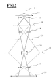
- the imaging properties described above between the objective lens (8) and the first projective lens (18) are illustrated graphically in FIG. 2 on the basis of the beam paths.
- an electrostatic phase plate (16) is shown in plan view.
- the phase plate (16) has an outer electron impermeable carrier (21) with a round hole (26).
- an annular electrode (23) with a central annular opening (24) is arranged centrically to the optical axis (OA).
- the annular electrode (23) is connected via two or three thin holding webs (22, 27) to the carrier (21).
- the orientation of the diffraction image relative to the phase plate (16) can be changed by the image rotation effected by this lens.
- essential diffraction reflexes (25) which fall on the holding webs (22, 27) can be moved on a circular path indicated by the dashed circle and thus rotate into a region in which they are undisturbed by a holding web (22, FIG. 27) can pass the phase plate.
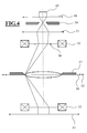
- the beam path in the case of generating a phase contrast with a conical illumination after US 6,797,956 shown.
- the zero beam in the object plane (49) is focused in the rear diffraction plane (50) of the objective (48) and imaged by the first diffraction lens (51) in the diffraction intermediate image plane (53).
- the first deflection system (52) near the intermediate image plane (56) annularly guides the beam over the phase shifting regions of an annular phase plate (57) in the diffraction imaging plane (53).
- the second diffraction lens (58) whose main plane lies in or near the diffraction intermediate image plane (53) then again generates an intermediate image of the object plane (49) in the input image plane of the first projective lens (54).
- the beam in the input image plane of the first projective lens (54) can be redirected back to the optical axis.
- phase plate arranged in the diffraction intermediate plane (53), a phase shift is imparted to the zero beam guided in a circular path, while the electrons which pass further away from the edge of the center opening of the phase plate and have been diffracted into higher diffraction orders in the object plane (49) the phase plate remain unaffected.
- the arrangement in FIG. 5 is essentially the same as the arrangement in FIG. 4. However, the arrangement in FIG. 5 has two phase plates.
- the first phase plate (58) is disposed in the rear diffraction plane (15) of the objective lens, and a second phase plate (57) is disposed in the conjugate image plane of the first diffraction lens (51) disposed in or near the main plane of the second diffraction lens (53 ) lies.
- the second diffractive lens forms the only real intermediate image of the object plane (49) between the first and second diffractive lenses (51, 53) into the input image plane of the projection system (54).
- the two phase plates (57, 58) are designed so that they each influence different, complementary to each other spatial areas of the diffraction patterns.
- the phase plate (58) arranged in the diffraction plane (15) of the objective produces a phase shift in the beam cone segment shown hatched in FIG. 5, while the second second phase plate (57) arranged in the diffraction intermediate image plane does not hatched beam cone segment generates a phase shift.
- the phase shift takes place here sequentially in the two diffraction images conjugated to one another, so that the desired phase shift between the zero beam and the diffracted beams results from the two contributions together. In principle, this way offers the possibility of realizing material-free and aberration-free electrostatic phase plates.
- both phase plates (57, 58) can each be formed so that any holding webs overall do not adversely affect the image formation. If only the scattered electrons with a half-plane phase plate experience a phase shift of ⁇ , then differential interference contrast can be produced.
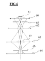
- FIG. 6 shows a somewhat different beam guidance with the embodiment already described with reference to FIGS. 1 and 2.
- the essential difference is that the objective lens (60) is excited so strongly that it already generates an intermediate image of the object plane (61) in or in the vicinity of the main plane of the first diffractive lens (62).
- the first diffraction lens (62) in turn forms the rear diffraction plane (65) of the objective lens (60) in or in the vicinity of the main plane of the second diffraction lens (63), so that there again Diffraction intermediate image plane arises.
- the phase-shifting element (67) is again arranged.
- the second diffraction lens (63) forms the intermediate image of the object plane (61) now formed in the main plane or in the vicinity of the main plane of the first diffraction lens into the input image plane (66) of the subsequent projection system (64).
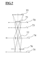
- FIG. 7 shows the beam path realized during operation of the system as a Lorenz microscope or at low magnification.
- the objective lens (70) When operating as Lorenzmikroskop the objective lens (70) is turned off, at low magnification (so-called low-Mag-mode), the objective lens is only slightly excited.
- the excitation of the first diffraction lens (73) is chosen so that its focal plane lies in the main plane of the second diffraction lens (74).
- the phase plate (77) is arranged in the main plane of the second diffraction lens.
- the second diffraction lens (74) generates in the input image plane (76) of the subsequent projective system (75) a real image of the virtual image (77) of the object plane (71) generated by the first diffraction lens (73).
- the projective (75) then generates an image magnified up to a factor of 10,000 of the object positioned in the object plane (71). This beam guidance thus allows a larger by about a factor of 5 maximum magnification over a conventional low
- the following can be estimated: at a focal length of the objective lens (8) of about 3 mm and a desired telescope magnification by a factor of 10 (since the objective lens (8) and the first diffraction lens (11) yes operated telescopically) results for the first diffraction lens (11) has a focal length of about 30 mm. It can be shown that in such a telescope system, the increase of the aperture error with respect to a system is negligible only with the objective lens.
- the first diffraction lens (11) must be spaced approximately 36 mm from the rear diffraction plane (10) of the objective lens (8) and between the first diffraction lens (11) and the second diffraction lens (15), a distance of 180 mm is required. Since the second diffraction lens (15) forms the intermediate image of the object plane (9) which arises in the rear focal plane (14) of the first diffractive lens (11) at a low magnification in the input image plane (17) of the projection system (18).
Landscapes
- Chemical & Material Sciences (AREA)
- Analytical Chemistry (AREA)
- Health & Medical Sciences (AREA)
- Nuclear Medicine, Radiotherapy & Molecular Imaging (AREA)
- Radiology & Medical Imaging (AREA)
- Physics & Mathematics (AREA)
- Life Sciences & Earth Sciences (AREA)
- Biochemistry (AREA)
- General Health & Medical Sciences (AREA)
- General Physics & Mathematics (AREA)
- Immunology (AREA)
- Pathology (AREA)
- Analysing Materials By The Use Of Radiation (AREA)
- Lenses (AREA)
Applications Claiming Priority (1)
| Application Number | Priority Date | Filing Date | Title |
|---|---|---|---|
| DE102006011615A DE102006011615A1 (de) | 2006-03-14 | 2006-03-14 | Phasenkontrast-Elektronenmikroskop |
Publications (4)
| Publication Number | Publication Date |
|---|---|
| EP1835523A2 true EP1835523A2 (fr) | 2007-09-19 |
| EP1835523A3 EP1835523A3 (fr) | 2008-03-05 |
| EP1835523B1 EP1835523B1 (fr) | 2016-06-29 |
| EP1835523B8 EP1835523B8 (fr) | 2016-09-28 |
Family
ID=38283520
Family Applications (1)
| Application Number | Title | Priority Date | Filing Date |
|---|---|---|---|
| EP07102803.9A Active EP1835523B8 (fr) | 2006-03-14 | 2007-02-21 | Microscope à électrons à contraste de phase |
Country Status (4)
| Country | Link |
|---|---|
| US (3) | US7741602B2 (fr) |
| EP (1) | EP1835523B8 (fr) |
| JP (1) | JP5116321B2 (fr) |
| DE (1) | DE102006011615A1 (fr) |
Families Citing this family (29)
| Publication number | Priority date | Publication date | Assignee | Title |
|---|---|---|---|---|
| DE102006055510B4 (de) * | 2006-11-24 | 2009-05-07 | Ceos Corrected Electron Optical Systems Gmbh | Phasenplatte, Bilderzeugungsverfahren und Elektronenmikroskop |
| DE102007007923A1 (de) * | 2007-02-14 | 2008-08-21 | Carl Zeiss Nts Gmbh | Phasenschiebendes Element und Teilchenstrahlgerät mit phasenschiebenden Element |
| EP2091062A1 (fr) * | 2008-02-13 | 2009-08-19 | FEI Company | TEM avec correcteur d'aberrations et lame de phase |
| EP2131385A1 (fr) * | 2008-06-05 | 2009-12-09 | FEI Company | Plaque de phase hybride |
| DE102008037698B4 (de) | 2008-08-14 | 2012-08-16 | Carl Zeiss Nts Gmbh | Elektronenmikroskop mit ringförmiger Beleuchtungsapertur |
| US7977633B2 (en) * | 2008-08-27 | 2011-07-12 | Max-Planck-Gesellschaft Zur Foerderung Der Wissenschaften E. V. | Phase plate, in particular for an electron microscope |
| DE102009001587A1 (de) * | 2009-01-06 | 2010-07-08 | Carl Zeiss Nts Gmbh | Verfahren zur Einstellung eines Betriebsparameters eines Teilchenstrahlgeräts sowie Probenhalter zur Durchführung des Verfahrens |
| DE102009010774A1 (de) * | 2009-02-26 | 2010-11-11 | Ceos Corrected Electron Optical Systems Gmbh | Verfahren und Vorrichtung zur Bildkontrasterzeugung durch Phasenschiebung |
| NL2004888A (en) * | 2009-06-29 | 2010-12-30 | Asml Netherlands Bv | Deposition method and apparatus. |
| WO2011071819A1 (fr) * | 2009-12-07 | 2011-06-16 | Regents Of The University Of California | Plaque de phase de cavité optique pour microscopie électronique à transmission |
| NL2006308C2 (en) | 2010-03-01 | 2013-05-27 | Zeiss Carl Nts Gmbh | Transmission electron microscope. |
| JP5564292B2 (ja) * | 2010-03-05 | 2014-07-30 | 株式会社日立製作所 | 位相板およびこれを用いた位相差電子顕微鏡 |
| WO2011163397A1 (fr) * | 2010-06-22 | 2011-12-29 | The Regents Of The University Of California | Ouverture de foucault passe-haut micro-usinée pour microscopie électronique |
| EP2413345B1 (fr) * | 2010-07-29 | 2013-02-20 | Carl Zeiss NTS GmbH | Système d'irradiation par particules chargées |
| US20120037815A1 (en) * | 2010-08-16 | 2012-02-16 | Yunn-Shin Shiue | Tem phase plate loading system |
| DE102011011751B4 (de) | 2011-02-18 | 2015-12-17 | Stiftung Caesar Center Of Advanced European Studies And Research | Halteanordnung zum Halten von Phasenkontrasteinheiten in einem Phasenkontrast-Elektronenmikroskop sowie Phasenkontrast-Elektronenmikroskop |
| DE102011014399B4 (de) | 2011-03-18 | 2017-08-03 | Stiftung Caesar Center Of Advanced European Studies And Research | Phasenplatte, Verfahren zum Herstellen einer Phasenplatte sowie Elektronenmikroskop |
| DE102011113645A1 (de) | 2011-09-19 | 2013-03-21 | Stiftung Caesar Center Of Advanced European Studies And Research | Verfahren zur Ausrichtung einer Phasenplatte in einem Elektronenmikroskop |
| JP6286270B2 (ja) | 2013-04-25 | 2018-02-28 | エフ イー アイ カンパニFei Company | 透過型電子顕微鏡内で位相版を用いる方法 |
| DE102013019297A1 (de) | 2013-11-19 | 2015-05-21 | Fei Company | Phasenplatte für ein Transmissionselektronenmikroskop |
| US10170274B2 (en) * | 2015-03-18 | 2019-01-01 | Battelle Memorial Institute | TEM phase contrast imaging with image plane phase grating |
| WO2016149676A1 (fr) | 2015-03-18 | 2016-09-22 | Battelle Memorial Institute | Masques à faisceau d'électrons pour des capteurs de compression |
| WO2017189212A1 (fr) | 2016-04-29 | 2017-11-02 | Battelle Memorial Institute | Spectroscopie à balayage comprimé |
| US10535497B2 (en) | 2016-08-22 | 2020-01-14 | Hitachi High-Technologies Corporation | Electron microscope and imaging method |
| US10295677B2 (en) | 2017-05-08 | 2019-05-21 | Battelle Memorial Institute | Systems and methods for data storage and retrieval |
| JP7193694B2 (ja) | 2018-07-26 | 2022-12-21 | 国立研究開発法人理化学研究所 | 電子顕微鏡およびそれを用いた試料観察方法 |
| JP7113399B2 (ja) * | 2019-03-05 | 2022-08-05 | N-Emラボラトリーズ株式会社 | 電子顕微鏡観察方法、透過型電子顕微鏡用絞り走査高速模倣装置、透過型電子顕微鏡及びデータ処理システム |
| US11237059B1 (en) * | 2020-12-14 | 2022-02-01 | Gerchberg Ophthalmic Dispensing, PLLC | Totagraphy: Coherent diffractive/digital information reconstruction by iterative phase recovery using special masks |
| EP4184136B1 (fr) * | 2021-11-18 | 2024-03-13 | Universität Stuttgart | Dispositif d'imagerie pour l'imagerie multispectrale ou hyperspectrale d'un objet |
Family Cites Families (23)
| Publication number | Priority date | Publication date | Assignee | Title |
|---|---|---|---|---|
| DE1049988B (fr) * | 1953-09-04 | |||
| US3493287A (en) * | 1966-04-26 | 1970-02-03 | Ibm | Optical detour phase system |
| US3566109A (en) * | 1968-02-15 | 1971-02-23 | Bell Telephone Labor Inc | Electron microscope method and apparatus for improving image phase contrast |
| DE1810818A1 (de) * | 1968-04-16 | 1969-10-23 | Prof Dr Walter Hoppe | Korpuskularstrahlgeraet mit einer Abbildungslinse und einer dieser zugeordneten phasenschiebenden Folie |
| CH678663A5 (fr) * | 1988-06-09 | 1991-10-15 | Zeiss Carl Fa | |
| DE3825103A1 (de) * | 1988-07-23 | 1990-01-25 | Zeiss Carl Fa | Verfahren zum beleuchten eines objektes in einem transmissions-elektronenmikroskop |
| DE4432811B4 (de) * | 1993-09-15 | 2006-04-13 | Carl Zeiss | Phasenkontrast-Röntgenmikroskop |
| JP3400541B2 (ja) * | 1994-06-14 | 2003-04-28 | 株式会社日立製作所 | 走査電子線を用いた磁性顕微方法及び走査型透過電子顕微鏡 |
| US5814815A (en) * | 1995-12-27 | 1998-09-29 | Hitachi, Ltd. | Phase-contrast electron microscope and phase plate therefor |
| JPH09237603A (ja) * | 1995-12-27 | 1997-09-09 | Hitachi Ltd | 位相差電子顕微鏡およびその位相板 |
| JPH11250850A (ja) * | 1998-03-02 | 1999-09-17 | Hitachi Ltd | 走査電子顕微鏡及び顕微方法並びに対話型入力装置 |
| JP4069545B2 (ja) * | 1999-05-19 | 2008-04-02 | 株式会社日立製作所 | 電子顕微方法及びそれを用いた電子顕微鏡並び生体試料検査方法及び生体検査装置 |
| DE19945344A1 (de) * | 1999-09-22 | 2001-03-29 | Leo Elektronenmikroskopie Gmbh | Teilchenoptisches Beleuchtungs- und Abbildungssystem mit einer Kondensor-Objektiv-Einfeldlinse |
| US6720558B2 (en) * | 2000-02-02 | 2004-04-13 | Jeol Ltd. | Transmission electron microscope equipped with energy filter |
| JP3544914B2 (ja) * | 2000-03-17 | 2004-07-21 | 住友化学工業株式会社 | 光学顕微鏡装置および顕微鏡観察方法。 |
| JP3773389B2 (ja) * | 2000-03-27 | 2006-05-10 | 日本電子株式会社 | 位相差電子顕微鏡用薄膜位相板並びに位相差電子顕微鏡及び位相板帯電防止法 |
| JP3942363B2 (ja) * | 2001-02-09 | 2007-07-11 | 日本電子株式会社 | 透過電子顕微鏡の位相板用レンズシステム、および透過電子顕微鏡 |
| JP3867524B2 (ja) * | 2001-07-05 | 2007-01-10 | 株式会社日立製作所 | 電子線を用いた観察装置及び観察方法 |
| JP4328044B2 (ja) * | 2001-09-25 | 2009-09-09 | 日本電子株式会社 | 差分コントラスト電子顕微鏡および電子顕微鏡像のデータ処理方法 |
| DE10200645A1 (de) * | 2002-01-10 | 2003-07-24 | Leo Elektronenmikroskopie Gmbh | Elektronenmikroskop mit ringförmiger Beleuchtungsapertur |
| US7601956B2 (en) * | 2003-09-02 | 2009-10-13 | Avilov Anatoly Sergeevich | Method for measuring diffraction patterns from a transmission electron microscopy to determine crystal structures and a device therefor |
| DE102007007923A1 (de) * | 2007-02-14 | 2008-08-21 | Carl Zeiss Nts Gmbh | Phasenschiebendes Element und Teilchenstrahlgerät mit phasenschiebenden Element |
| EP2091062A1 (fr) | 2008-02-13 | 2009-08-19 | FEI Company | TEM avec correcteur d'aberrations et lame de phase |
-
2006
- 2006-03-14 DE DE102006011615A patent/DE102006011615A1/de not_active Withdrawn
-
2007
- 2007-02-21 EP EP07102803.9A patent/EP1835523B8/fr active Active
- 2007-03-09 JP JP2007060060A patent/JP5116321B2/ja not_active Expired - Fee Related
- 2007-03-13 US US11/717,201 patent/US7741602B2/en active Active
-
2010
- 2010-03-19 US US12/659,751 patent/US8039796B2/en active Active
-
2011
- 2011-10-14 US US13/274,066 patent/US8330105B2/en not_active Expired - Fee Related
Also Published As
| Publication number | Publication date |
|---|---|
| DE102006011615A1 (de) | 2007-09-20 |
| US7741602B2 (en) | 2010-06-22 |
| JP5116321B2 (ja) | 2013-01-09 |
| EP1835523B8 (fr) | 2016-09-28 |
| EP1835523B1 (fr) | 2016-06-29 |
| US8039796B2 (en) | 2011-10-18 |
| US20070284528A1 (en) | 2007-12-13 |
| US8330105B2 (en) | 2012-12-11 |
| US20120049062A1 (en) | 2012-03-01 |
| US20100181481A1 (en) | 2010-07-22 |
| EP1835523A3 (fr) | 2008-03-05 |
| JP2007250541A (ja) | 2007-09-27 |
Similar Documents
| Publication | Publication Date | Title |
|---|---|---|
| EP1835523B1 (fr) | Microscope à électrons à contraste de phase | |
| EP1959475B1 (fr) | Elément à décalage de phase et appareil de rayonnement à particules doté d'un élément de à décalage de phase | |
| EP1329936B1 (fr) | Microscope électronique à contraste de phase avec ouverture d'illumination annulaire | |
| DE69432098T2 (de) | Elektronenstrahl-Lithographie-System | |
| EP2461346B1 (fr) | Appareil à faisceau de particules doté d'un système de déviation | |
| DE102008037698B4 (de) | Elektronenmikroskop mit ringförmiger Beleuchtungsapertur | |
| EP3712924B1 (fr) | Dispositif et procédé de transfert d'électrons d'un échantillon à un analyseur d'énergie et dispositif spectromètre d'électrons | |
| EP3811394A2 (fr) | Système à faisceau de particules | |
| DE102020123567B4 (de) | Vielzahl-Teilchenstrahl-System mit Kontrast-Korrektur-Linsen-System | |
| DE4129403A1 (de) | Abbildungssystem fuer strahlung geladener teilchen mit spiegelkorrektor | |
| DE112011104595B4 (de) | Vorrichtung mit einem geladenen Teilchenstrahl sowie Verfahren zur Steuerung | |
| EP2159818B1 (fr) | Microscope à électrons avec une lame de phase | |
| EP0899771B1 (fr) | Filtre en énergie, en particulier pour microscope électronique | |
| EP0967630A2 (fr) | Microscope électronique avec filtre magnétique pour l'obtention d'images | |
| DE102009016861A1 (de) | Teilchenstrahlmikroskop | |
| EP0911860B1 (fr) | Appareil à faisceau de particules chargées avec filtre en énergie | |
| DE102015210893B4 (de) | Analyseeinrichtung zur Analyse der Energie geladener Teilchen und Teilchenstrahlgerät mit einer Analyseeinrichtung | |
| EP1006556B1 (fr) | APPAREIL D'OPTIQUE PARTICULAIRE pour la fabrication de microstructures | |
| DE10235981B4 (de) | Teilchenoptische Vorrichtung und Elektronenmikroskop | |
| DE2742264C3 (de) | Verfahren zur Abbildung eines Objektes mit geringer Vergrößerung mittels eines Korpuskularstrahlgeräts, insbesondere eines Elektronen-Mikroskops und Korpuskularstrahlgerät zur Durchführung des Verfahrens | |
| DE2043749C3 (de) | Raster-Korpuskularstrahlmikroskop | |
| DE60037071T2 (de) | Magentischer Energiefilter | |
| EP1087420A2 (fr) | Dispositif d'optique corpusculaire pour l'illumination et l'imagerie comprenant une lentille condenseur-objectif à champ unique | |
| DE102014019408B4 (de) | Abbildende Energiefiltervorrichtung und Verfahren zu deren Betrieb | |
| EP0847075A2 (fr) | Source de positrons |
Legal Events
| Date | Code | Title | Description |
|---|---|---|---|
| PUAI | Public reference made under article 153(3) epc to a published international application that has entered the european phase |
Free format text: ORIGINAL CODE: 0009012 |
|
| AK | Designated contracting states |
Kind code of ref document: A2 Designated state(s): AT BE BG CH CY CZ DE DK EE ES FI FR GB GR HU IE IS IT LI LT LU LV MC NL PL PT RO SE SI SK TR |
|
| AX | Request for extension of the european patent |
Extension state: AL BA HR MK YU |
|
| PUAL | Search report despatched |
Free format text: ORIGINAL CODE: 0009013 |
|
| AK | Designated contracting states |
Kind code of ref document: A3 Designated state(s): AT BE BG CH CY CZ DE DK EE ES FI FR GB GR HU IE IS IT LI LT LU LV MC NL PL PT RO SE SI SK TR |
|
| AX | Request for extension of the european patent |
Extension state: AL BA HR MK YU |
|
| 17P | Request for examination filed |
Effective date: 20080424 |
|
| 17Q | First examination report despatched |
Effective date: 20080716 |
|
| AKX | Designation fees paid |
Designated state(s): CZ DE GB NL |
|
| REG | Reference to a national code |
Ref country code: DE Ref legal event code: R079 Ref document number: 502007014907 Country of ref document: DE Free format text: PREVIOUS MAIN CLASS: H01J0037260000 Ipc: G01N0023040000 |
|
| RIC1 | Information provided on ipc code assigned before grant |
Ipc: H01J 37/26 20060101ALI20151012BHEP Ipc: G01N 23/04 20060101AFI20151012BHEP Ipc: H01J 37/04 20060101ALI20151012BHEP |
|
| GRAP | Despatch of communication of intention to grant a patent |
Free format text: ORIGINAL CODE: EPIDOSNIGR1 |
|
| INTG | Intention to grant announced |
Effective date: 20160302 |
|
| GRAS | Grant fee paid |
Free format text: ORIGINAL CODE: EPIDOSNIGR3 |
|
| GRAA | (expected) grant |
Free format text: ORIGINAL CODE: 0009210 |
|
| AK | Designated contracting states |
Kind code of ref document: B1 Designated state(s): CZ DE GB NL |
|
| REG | Reference to a national code |
Ref country code: GB Ref legal event code: FG4D Free format text: NOT ENGLISH |
|
| GRAT | Correction requested after decision to grant or after decision to maintain patent in amended form |
Free format text: ORIGINAL CODE: EPIDOSNCDEC |
|
| REG | Reference to a national code |
Ref country code: DE Ref legal event code: R096 Ref document number: 502007014907 Country of ref document: DE |
|
| RAP2 | Party data changed (patent owner data changed or rights of a patent transferred) |
Owner name: CARL ZEISS MICROSCOPY GMBH |
|
| REG | Reference to a national code |
Ref country code: NL Ref legal event code: FP |
|
| REG | Reference to a national code |
Ref country code: DE Ref legal event code: R097 Ref document number: 502007014907 Country of ref document: DE |
|
| PLBE | No opposition filed within time limit |
Free format text: ORIGINAL CODE: 0009261 |
|
| STAA | Information on the status of an ep patent application or granted ep patent |
Free format text: STATUS: NO OPPOSITION FILED WITHIN TIME LIMIT |
|
| 26N | No opposition filed |
Effective date: 20170330 |
|
| GBPC | Gb: european patent ceased through non-payment of renewal fee |
Effective date: 20170221 |
|
| PG25 | Lapsed in a contracting state [announced via postgrant information from national office to epo] |
Ref country code: GB Free format text: LAPSE BECAUSE OF NON-PAYMENT OF DUE FEES Effective date: 20170221 |
|
| PGFP | Annual fee paid to national office [announced via postgrant information from national office to epo] |
Ref country code: NL Payment date: 20250218 Year of fee payment: 19 |
|
| PGFP | Annual fee paid to national office [announced via postgrant information from national office to epo] |
Ref country code: DE Payment date: 20250218 Year of fee payment: 19 |
|
| PGFP | Annual fee paid to national office [announced via postgrant information from national office to epo] |
Ref country code: CZ Payment date: 20250213 Year of fee payment: 19 |