EP0847085A2 - Procédé et appareil pour le serrage mécanique et électrostatique d'un substrat - Google Patents
Procédé et appareil pour le serrage mécanique et électrostatique d'un substrat Download PDFInfo
- Publication number
- EP0847085A2 EP0847085A2 EP97309775A EP97309775A EP0847085A2 EP 0847085 A2 EP0847085 A2 EP 0847085A2 EP 97309775 A EP97309775 A EP 97309775A EP 97309775 A EP97309775 A EP 97309775A EP 0847085 A2 EP0847085 A2 EP 0847085A2
- Authority
- EP
- European Patent Office
- Prior art keywords
- pedestal
- workpiece
- wafer
- center
- clamping
- Prior art date
- Legal status (The legal status is an assumption and is not a legal conclusion. Google has not performed a legal analysis and makes no representation as to the accuracy of the status listed.)
- Withdrawn
Links
Images


Classifications
-
- H—ELECTRICITY
- H10—SEMICONDUCTOR DEVICES; ELECTRIC SOLID-STATE DEVICES NOT OTHERWISE PROVIDED FOR
- H10P—GENERIC PROCESSES OR APPARATUS FOR THE MANUFACTURE OR TREATMENT OF DEVICES COVERED BY CLASS H10
- H10P72/00—Handling or holding of wafers, substrates or devices during manufacture or treatment thereof
- H10P72/70—Handling or holding of wafers, substrates or devices during manufacture or treatment thereof for supporting or gripping
- H10P72/76—Handling or holding of wafers, substrates or devices during manufacture or treatment thereof for supporting or gripping using mechanical means, e.g. clamps or pinches
-
- H—ELECTRICITY
- H10—SEMICONDUCTOR DEVICES; ELECTRIC SOLID-STATE DEVICES NOT OTHERWISE PROVIDED FOR
- H10P—GENERIC PROCESSES OR APPARATUS FOR THE MANUFACTURE OR TREATMENT OF DEVICES COVERED BY CLASS H10
- H10P72/00—Handling or holding of wafers, substrates or devices during manufacture or treatment thereof
- H10P72/70—Handling or holding of wafers, substrates or devices during manufacture or treatment thereof for supporting or gripping
- H10P72/72—Handling or holding of wafers, substrates or devices during manufacture or treatment thereof for supporting or gripping using electrostatic chucks
- H10P72/722—Details of electrostatic chucks
Definitions
- the invention relates generally to chucks for holding a wafer and, more specifically, to an improved chuck for clamping large diameter (300mm or more) wafers containing a mechanical clamp for clamping the periphery of the wafer and an electrostatic clamp for clamping the center of the wafer.
- Chucks either mechanical or electrostatic, are used for holding a workpiece in various applications ranging from holding a sheet of paper in a computer graphics plotter to holding a wafer within a semiconductor wafer process chamber.
- Mechanical chucks typically secure a workpiece, i.e., semiconductor wafer, to the chuck by applying a physical holding force to a clamping ring or calipers located at the periphery of the wafer. The wafer is held in place until the physical force is reversed and the clamping ring or calipers retract.
- Electrostatic chucks perform this task by creating an electrostatic attractive force between the wafer and the chuck. A voltage is applied to one or more electrodes in the chuck so as to induce opposite polarity charges in the wafer and electrodes, respectively. The opposite charges pull the wafer against the chuck, thereby retaining the wafer.
- a diameter of 200mm is an accepted industry standard for semiconductor wafer size.
- semiconductor wafer processing equipment either type of chuck (mechanical or electrostatic) is used for clamping 200mm wafers to a pedestal during processing.
- a 200mm wafer is mechanically clamped to the pedestal to ensure that the wafer is stationary during processing.
- the pedestal is heated to heat the wafer to an appropriate temperature to facilitate efficient processing.
- Increased demand for 200mm wafers led to improvements in chuck construction and features for processing this size substrate. This resulted in higher yields, better temperature control and an overall better quality product.
- FIG. 1 depicts a conventional PVD chamber 100 for processing 300mm semiconductor wafers.
- the wafer 102 rests on support surface 105 of a pedestal 104.
- the pedestal 104 is supported by a pedestal base 106 which contains the necessary wiring to conduct power from a remote power source (not shown) to the heating elements (not shown) within the pedestal 104.
- the wafer 102 is mechanically clamped to the pedestal 104 by a peripheral clamping ring 108.
- Lift pins 110 mounted on a platform 112 connected to a vertical shaft 114 serve to lift the wafer 102 off the pedestal surface 105 after processing.
- a heat transfer gas is pumped into the region 113 between the wafer 102 and support surface 105 until an optimal pressure for heat transfer is reached.
- the bowing of the wafer resulting from the backside gas pressure is seen in the circled portion of FIG. 1.
- This condition causes a loss of contact area between the wafer and the pedestal as well as non-uniform distribution of heat transfer gas.
- This in turn contributes to a non-uniform temperature profile across the wafer and may also lead to stress fractures in the substrate material. Maintaining a uniform temperature across the wafer is necessary and important to ensure high performance and yield of the end product. Consequently, processing a 300mm wafer under these conditions may lead to process irregularities and wafer damage.
- the disadvantages heretofore associated with the prior art are overcome by an improved chuck for retaining a wafer in a semiconductor wafer processing system.
- the inventive chuck combines both mechanical and electrostatic chucking techniques to secure a large diameter wafer to a pedestal.
- the inventive apparatus consists of a pedestal for supporting a wafer, a mechanical clamping portion for mechanically clamping the wafer at its periphery and an electrostatic clamping portion for electrostatically clamping the wafer at its center.
- the mechanical clamping portion can be a clamping ring located above the periphery of the pedestal or some other apparatus for mechanically clamping the peripheral edge of the wafer.
- the electrostatic clamping portion contains one or more electrodes encased in a dielectric material and positioned proximate the center of the pedestal surface.
- the pedestal surface contains a centrally located recess within which the electrostatic clamping portion is located.
- the "mini" electrostatic chuck is secured to the recess by an annular clamping ring bolted to the pedestal. A region of the bottom of the electrode(s) is exposed to facilitate electrical connection to the electrode(s).
- the apparatus also contains grooves for heat transfer gas distribution. These grooves are located about the periphery of the chuck and extend radially inward, stopping at the electrostatic clamping portion. The grooves are supplied heat transfer gas via conduits extending through the pedestal.
- a wafer is positioned upon the pedestal surface using a conventional robotic wafer transport assembly.
- the wafer is first mechanically clamped at its periphery to the pedestal and then electrostatically clamped to the pedestal at its center. Once clamped, the invention applies a heat transfer gas between the wafer and the pedestal.
- This invention fulfills the long felt need for a method and apparatus that can effectively clamp a large (300mm diameter) wafer to a chuck and provide heat transfer characteristics similar to those found in semiconductor wafer processing systems that process smaller diameter wafers.
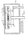
- FIG. 2 depicts a cross-sectional view of the inventive chuck adapted to both mechanically and electrostatically clamp a wafer 202 to a pedestal 204 within a process chamber 200 of a semiconductor wafer processing system, e.g., a PVD system.
- a semiconductor wafer processing system e.g., a PVD system.
- the pedestal 204 is constructed from a heat conductive metal, i.e., stainless steel or copper.
- the pedestal 204 is provided with a bipolar electrostatic chuck assembly 216 located at the center of the pedestal 204.
- the electrostatic chuck assembly has a wafer support surface that is positioned substantially flush with a pedestal surface 205 (a wafer support surface).
- the electrostatic chuck assembly 216 creates an electric field at the center of the pedestal 204 which draws the center of a 300mm wafer toward the pedestal surface 205 to eliminate wafer bowing.
- the electrostatic chuck assembly 216 contains two electrodes 402 (generally a pair of half-moon shaped, coplanar conductors) encased in a circular slab of dielectric material 404.
- the dielectric material is preferably ceramic.
- the electrostatic chuck assembly 216 rests inside a recessed portion 405 of the pedestal surface 205.
- the pedestal 204 is provided with two electric leads 406 that contact the bottom of each of the bipolar electrodes 402.
- the electric leads conduct a voltage from a remote voltage source (not shown) through the pedestal base 206 to the bipolar electrodes 402. To facilitate clamping, a positive voltage is applied to one electrode and a negative voltage is applied to the other electrode.
- an annular clamp 408 is provided to engage a lip 410 of the electrostatic chuck assembly 216.
- a localized electric field is established at the center of the pedestal 204. Specifically, an electric field is produced between the electrodes and couples to the underside of the wafer. As charges accumulate on the underside of the wafer, the electric field draws the wafer 202 toward the pedestal surface 205 for increased contact with the surface. Such wafer-to-pedestal contact results in increased heat conduction between the wafer and pedestal.
- a heat transfer gas is pumped into the interstitial spaces between the wafer 202 and the pedestal surface 205.
- the gas is pumped beneath the wafer via inlet ports 409.
- Gas distribution grooves 218 are formed in the pedestal surface and connected to the inlet ports. Although various groove patterns could be used, illustratively, the grooves extend radially outwards from the clamp 408 at four evenly spaced locations.
- a gas distribution groove is also provided at the periphery of the pedestal 204 to interconnect each radially extending groove.
- the electrostatic chuck assembly could be of any form of electrostatic chuck.
- the electrostatic chuck assembly could be unipolar, e.g., having a single electrode.
- the electrostatic chuck assembly does not have to reside within a recessed area of the pedestal.
- the electrostatic chuck could be a flex circuit type chuck having one or more electrodes sandwiched between a pair of dielectric layers (e.g., polyimide layers). The flexible assembly is then adhered to the surface of the pedestal near the center thereof using an adhesive.
- FIG. 4 shows a top view of the preferred embodiment of the pedestal 204.
- the electrostatic chuck assembly 216 is circular, with a corresponding annular clamp 408 circumscribing its periphery.
- the clamp is secured at four points by bolts 412 communicating with threaded bores (not shown) in the pedestal surface 205.
- the gas distribution grooves 218 do not totally extend to the center of the pedestal. As such, a lower volume of gas is introduced to the center which will also reduce the wafer's tendency to bow.
- the device is extremely effective, in that it reduces bowing at precisely the point where additional clamping is required the most, namely, the center of the wafer. Additionally, the simplicity in its design make it cost-effective to manufacture and incorporate into existing pedestal designs.
Landscapes
- Container, Conveyance, Adherence, Positioning, Of Wafer (AREA)
- Drying Of Semiconductors (AREA)
- Jigs For Machine Tools (AREA)
Applications Claiming Priority (2)
| Application Number | Priority Date | Filing Date | Title |
|---|---|---|---|
| US08/758,829 US5885428A (en) | 1996-12-04 | 1996-12-04 | Method and apparatus for both mechanically and electrostatically clamping a wafer to a pedestal within a semiconductor wafer processing system |
| US758829 | 1996-12-04 |
Publications (2)
| Publication Number | Publication Date |
|---|---|
| EP0847085A2 true EP0847085A2 (fr) | 1998-06-10 |
| EP0847085A3 EP0847085A3 (fr) | 2000-01-05 |
Family
ID=25053274
Family Applications (1)
| Application Number | Title | Priority Date | Filing Date |
|---|---|---|---|
| EP97309775A Withdrawn EP0847085A3 (fr) | 1996-12-04 | 1997-12-04 | Procédé et appareil pour le serrage mécanique et électrostatique d'un substrat |
Country Status (6)
| Country | Link |
|---|---|
| US (1) | US5885428A (fr) |
| EP (1) | EP0847085A3 (fr) |
| JP (1) | JPH10313044A (fr) |
| KR (1) | KR19980063620A (fr) |
| SG (1) | SG105448A1 (fr) |
| TW (1) | TW343370B (fr) |
Cited By (5)
| Publication number | Priority date | Publication date | Assignee | Title |
|---|---|---|---|---|
| WO2000019492A3 (fr) * | 1998-09-30 | 2000-11-16 | Applied Materials Inc | Ensemble cathodes contenant un mandrin electrostatique destine a retenir une plaquette dans un systeme de traitement de plaquettes a semi-conducteur |
| WO2004038766A3 (fr) * | 2002-10-23 | 2004-07-22 | Axcelis Tech Inc | Structure de support de tranche comprenant un support electrostatique et plaque superieure assurant une protection laterale et une evacuation des gaz |
| US20110299217A1 (en) * | 2010-06-08 | 2011-12-08 | Axcelis Technologies, Inc. | Heated electrostatic chuck including mechanical clamp capability at high temperature |
| WO2011155986A1 (fr) * | 2010-06-08 | 2011-12-15 | Axcelis Technologies Inc. | Support électrostatique chauffé comprenant une capacité de serrage mécanique à haute température |
| EP4423790A4 (fr) * | 2021-10-26 | 2026-02-11 | Applied Materials Inc | Mandrin pour le traitement de pièces semi-conductrices à des températures élevées |
Families Citing this family (35)
| Publication number | Priority date | Publication date | Assignee | Title |
|---|---|---|---|---|
| KR100308209B1 (ko) * | 1998-06-20 | 2001-11-30 | 윤종용 | 리플로우공정을 위한 히터 어셈블리의 클램프 |
| US6123804A (en) * | 1999-02-22 | 2000-09-26 | Applied Materials, Inc. | Sectional clamp ring |
| US6165276A (en) * | 1999-09-17 | 2000-12-26 | United Microelectronics Corp. | Apparatus for preventing plasma etching of a wafer clamp in semiconductor fabrication processes |
| JP2002270346A (ja) * | 2001-03-09 | 2002-09-20 | Mitsubishi Heavy Ind Ltd | 加熱装置及びその製造方法並びに被膜形成装置 |
| KR20030026387A (ko) * | 2001-09-12 | 2003-04-03 | 주식회사 아이앤에스 | 반도체 웨이퍼의 화학기상증착공정중에 사용되는받침히터와 그 제조방법 |
| KR100504426B1 (ko) * | 2002-05-13 | 2005-07-28 | 최성문 | 이동식 교량 점검 장치 |
| US7506593B2 (en) * | 2002-10-23 | 2009-03-24 | Kinetics Systems, Inc. | Microfabrication tool pedestal and method of use |
| US7910218B2 (en) | 2003-10-22 | 2011-03-22 | Applied Materials, Inc. | Cleaning and refurbishing chamber components having metal coatings |
| US7102871B2 (en) * | 2003-10-29 | 2006-09-05 | Taiwan Semiconductor Manufacturing Co,, Ltd. | Electrostatic chuck assembly having disassembling device |
| US20060096857A1 (en) * | 2004-11-08 | 2006-05-11 | Ilya Lavitsky | Physical vapor deposition chamber having a rotatable substrate pedestal |
| US20060096851A1 (en) * | 2004-11-08 | 2006-05-11 | Ilya Lavitsky | Physical vapor deposition chamber having an adjustable target |
| JP4869610B2 (ja) * | 2005-03-17 | 2012-02-08 | 東京エレクトロン株式会社 | 基板保持部材及び基板処理装置 |
| US8617672B2 (en) | 2005-07-13 | 2013-12-31 | Applied Materials, Inc. | Localized surface annealing of components for substrate processing chambers |
| US7762114B2 (en) | 2005-09-09 | 2010-07-27 | Applied Materials, Inc. | Flow-formed chamber component having a textured surface |
| US20070181420A1 (en) * | 2006-02-07 | 2007-08-09 | Ming-Tung Wang | Wafer stage having an encapsulated central pedestal plate |
| US7718045B2 (en) * | 2006-06-27 | 2010-05-18 | Applied Materials, Inc. | Ground shield with reentrant feature |
| JP4642789B2 (ja) * | 2006-07-14 | 2011-03-02 | セイコーエプソン株式会社 | 成膜装置及び成膜方法 |
| US7981262B2 (en) | 2007-01-29 | 2011-07-19 | Applied Materials, Inc. | Process kit for substrate processing chamber |
| US7942969B2 (en) * | 2007-05-30 | 2011-05-17 | Applied Materials, Inc. | Substrate cleaning chamber and components |
| US20090084317A1 (en) * | 2007-09-28 | 2009-04-02 | Applied Materials, Inc. | Atomic layer deposition chamber and components |
| US9478428B2 (en) | 2010-10-05 | 2016-10-25 | Skyworks Solutions, Inc. | Apparatus and methods for shielding a plasma etcher electrode |
| US20120083129A1 (en) | 2010-10-05 | 2012-04-05 | Skyworks Solutions, Inc. | Apparatus and methods for focusing plasma |
| US9768052B2 (en) | 2013-03-14 | 2017-09-19 | Applied Materials, Inc. | Minimal contact edge ring for rapid thermal processing |
| US10546768B2 (en) | 2015-02-25 | 2020-01-28 | Corning Incorporated | Apparatus and method to electrostatically chuck substrates to a moving carrier |
| CN108369922B (zh) | 2016-01-26 | 2023-03-21 | 应用材料公司 | 晶片边缘环升降解决方案 |
| CN116110846A (zh) | 2016-01-26 | 2023-05-12 | 应用材料公司 | 晶片边缘环升降解决方案 |
| US10553404B2 (en) | 2017-02-01 | 2020-02-04 | Applied Materials, Inc. | Adjustable extended electrode for edge uniformity control |
| US11075105B2 (en) | 2017-09-21 | 2021-07-27 | Applied Materials, Inc. | In-situ apparatus for semiconductor process module |
| US11043400B2 (en) * | 2017-12-21 | 2021-06-22 | Applied Materials, Inc. | Movable and removable process kit |
| US20190244787A1 (en) * | 2018-02-02 | 2019-08-08 | Wei-Chuan Chou | Plasma etching reaction chamber |
| US11201037B2 (en) | 2018-05-28 | 2021-12-14 | Applied Materials, Inc. | Process kit with adjustable tuning ring for edge uniformity control |
| US11935773B2 (en) | 2018-06-14 | 2024-03-19 | Applied Materials, Inc. | Calibration jig and calibration method |
| US11289310B2 (en) | 2018-11-21 | 2022-03-29 | Applied Materials, Inc. | Circuits for edge ring control in shaped DC pulsed plasma process device |
| WO2020214327A1 (fr) | 2019-04-19 | 2020-10-22 | Applied Materials, Inc. | Retrait d'anneau d'une chambre de traitement |
| US12009236B2 (en) | 2019-04-22 | 2024-06-11 | Applied Materials, Inc. | Sensors and system for in-situ edge ring erosion monitor |
Family Cites Families (7)
| Publication number | Priority date | Publication date | Assignee | Title |
|---|---|---|---|---|
| US4412133A (en) * | 1982-01-05 | 1983-10-25 | The Perkin-Elmer Corp. | Electrostatic cassette |
| JPS6060060A (ja) * | 1983-09-12 | 1985-04-06 | 株式会社日立製作所 | 鉄道車両の扉開閉装置 |
| US4692836A (en) * | 1983-10-31 | 1987-09-08 | Toshiba Kikai Kabushiki Kaisha | Electrostatic chucks |
| JPH0730468B2 (ja) * | 1988-06-09 | 1995-04-05 | 日電アネルバ株式会社 | ドライエッチング装置 |
| JP2748127B2 (ja) * | 1988-09-02 | 1998-05-06 | キヤノン株式会社 | ウエハ保持方法 |
| US5350479A (en) * | 1992-12-02 | 1994-09-27 | Applied Materials, Inc. | Electrostatic chuck for high power plasma processing |
| US5591269A (en) * | 1993-06-24 | 1997-01-07 | Tokyo Electron Limited | Vacuum processing apparatus |
-
1996
- 1996-12-04 US US08/758,829 patent/US5885428A/en not_active Expired - Lifetime
-
1997
- 1997-11-26 SG SG9704148A patent/SG105448A1/en unknown
- 1997-11-27 KR KR1019970063305A patent/KR19980063620A/ko not_active Withdrawn
- 1997-11-28 TW TW086117960A patent/TW343370B/zh active
- 1997-12-04 EP EP97309775A patent/EP0847085A3/fr not_active Withdrawn
- 1997-12-04 JP JP9366563A patent/JPH10313044A/ja not_active Withdrawn
Cited By (10)
| Publication number | Priority date | Publication date | Assignee | Title |
|---|---|---|---|---|
| WO2000019492A3 (fr) * | 1998-09-30 | 2000-11-16 | Applied Materials Inc | Ensemble cathodes contenant un mandrin electrostatique destine a retenir une plaquette dans un systeme de traitement de plaquettes a semi-conducteur |
| US6219219B1 (en) * | 1998-09-30 | 2001-04-17 | Applied Materials, Inc. | Cathode assembly containing an electrostatic chuck for retaining a wafer in a semiconductor wafer processing system |
| WO2004038766A3 (fr) * | 2002-10-23 | 2004-07-22 | Axcelis Tech Inc | Structure de support de tranche comprenant un support electrostatique et plaque superieure assurant une protection laterale et une evacuation des gaz |
| US20110299217A1 (en) * | 2010-06-08 | 2011-12-08 | Axcelis Technologies, Inc. | Heated electrostatic chuck including mechanical clamp capability at high temperature |
| WO2011155986A1 (fr) * | 2010-06-08 | 2011-12-15 | Axcelis Technologies Inc. | Support électrostatique chauffé comprenant une capacité de serrage mécanique à haute température |
| CN102934218A (zh) * | 2010-06-08 | 2013-02-13 | 艾克塞利斯科技公司 | 高温下具有机械夹持能力的受热静电夹头 |
| US8797706B2 (en) | 2010-06-08 | 2014-08-05 | Axcelis Technologies, Inc. | Heated annulus chuck |
| US8941968B2 (en) * | 2010-06-08 | 2015-01-27 | Axcelis Technologies, Inc. | Heated electrostatic chuck including mechanical clamp capability at high temperature |
| CN102934218B (zh) * | 2010-06-08 | 2016-05-04 | 艾克塞利斯科技公司 | 高温下具有机械夹持能力的受热静电夹头 |
| EP4423790A4 (fr) * | 2021-10-26 | 2026-02-11 | Applied Materials Inc | Mandrin pour le traitement de pièces semi-conductrices à des températures élevées |
Also Published As
| Publication number | Publication date |
|---|---|
| TW343370B (en) | 1998-10-21 |
| EP0847085A3 (fr) | 2000-01-05 |
| SG105448A1 (en) | 2004-08-27 |
| KR19980063620A (ko) | 1998-10-07 |
| JPH10313044A (ja) | 1998-11-24 |
| US5885428A (en) | 1999-03-23 |
Similar Documents
| Publication | Publication Date | Title |
|---|---|---|
| US5885428A (en) | Method and apparatus for both mechanically and electrostatically clamping a wafer to a pedestal within a semiconductor wafer processing system | |
| US10867832B2 (en) | Apparatus for holding semiconductor wafers | |
| JP3943188B2 (ja) | ワークピースを保持する装置および方法 | |
| US11742781B2 (en) | Electrostatic chuck with charge dissipation coating | |
| JP5464655B2 (ja) | 環状固定及び背面冷却を行う静電クランプ | |
| US5880923A (en) | Method and apparatus for improved retention of a semiconductor wafer within a semiconductor wafer processing system | |
| US6117246A (en) | Conductive polymer pad for supporting a workpiece upon a workpiece support surface of an electrostatic chuck | |
| KR100369106B1 (ko) | 다층의정전식척및그제조방법 | |
| US5885469A (en) | Topographical structure of an electrostatic chuck and method of fabricating same | |
| US6034863A (en) | Apparatus for retaining a workpiece in a process chamber within a semiconductor wafer processing system | |
| US5745332A (en) | Monopolar electrostatic chuck having an electrode in contact with a workpiece | |
| JP2662106B2 (ja) | ウェーハを処理する装置 | |
| KR20170124620A (ko) | 인-시츄 제거 가능한 정전 척 | |
| KR20050092749A (ko) | 기판 처리용 장치 | |
| JP2024541352A (ja) | Pvdチャンバ用高温着脱式超高周波(vhf)静電チャック(esc) | |
| KR100714667B1 (ko) | 웨이퍼 연마 헤드 및 연마 방법 | |
| KR20140007422A (ko) | 마찰전기 전하 제어 정전기 클램프 | |
| JPH11111830A (ja) | 静電吸着装置および静電吸着方法、ならびにそれを用いた処理装置および処理方法 | |
| EP0460954B1 (fr) | Serrage de la pièce à usiner | |
| US20240096594A1 (en) | System for etching with a plasma | |
| KR20240121531A (ko) | 기판 처리 장치 및 이를 이용한 기판 처리 방법 |
Legal Events
| Date | Code | Title | Description |
|---|---|---|---|
| PUAI | Public reference made under article 153(3) epc to a published international application that has entered the european phase |
Free format text: ORIGINAL CODE: 0009012 |
|
| AK | Designated contracting states |
Kind code of ref document: A2 Designated state(s): AT BE CH DE DK ES FI FR GB GR IE IT LI LU MC NL PT SE |
|
| AX | Request for extension of the european patent |
Free format text: AL;LT;LV;MK;RO;SI |
|
| PUAL | Search report despatched |
Free format text: ORIGINAL CODE: 0009013 |
|
| RIC1 | Information provided on ipc code assigned before grant |
Free format text: 6H 01L 21/68 A, 6H 01L 21/00 B |
|
| AK | Designated contracting states |
Kind code of ref document: A3 Designated state(s): AT BE CH DE DK ES FI FR GB GR IE IT LI LU MC NL PT SE |
|
| AX | Request for extension of the european patent |
Free format text: AL;LT;LV;MK;RO;SI |
|
| AKX | Designation fees paid | ||
| REG | Reference to a national code |
Ref country code: DE Ref legal event code: 8566 |
|
| STAA | Information on the status of an ep patent application or granted ep patent |
Free format text: STATUS: THE APPLICATION IS DEEMED TO BE WITHDRAWN |
|
| 18D | Application deemed to be withdrawn |
Effective date: 20000706 |