EP0849601B1 - Appareil et procédé pour déterminer le signe d'un décalage de phase entre deux signaux électriques - Google Patents
Appareil et procédé pour déterminer le signe d'un décalage de phase entre deux signaux électriques Download PDFInfo
- Publication number
- EP0849601B1 EP0849601B1 EP97120612A EP97120612A EP0849601B1 EP 0849601 B1 EP0849601 B1 EP 0849601B1 EP 97120612 A EP97120612 A EP 97120612A EP 97120612 A EP97120612 A EP 97120612A EP 0849601 B1 EP0849601 B1 EP 0849601B1
- Authority
- EP
- European Patent Office
- Prior art keywords
- signal
- sign
- receiving
- comparator
- trigger
- Prior art date
- Legal status (The legal status is an assumption and is not a legal conclusion. Google has not performed a legal analysis and makes no representation as to the accuracy of the status listed.)
- Expired - Lifetime
Links
- 230000010363 phase shift Effects 0.000 title claims description 36
- 238000000034 method Methods 0.000 title description 3
- 239000004020 conductor Substances 0.000 claims description 49
- 230000002123 temporal effect Effects 0.000 claims description 26
- 238000010079 rubber tapping Methods 0.000 claims description 10
- 238000012545 processing Methods 0.000 claims description 8
- 230000000737 periodic effect Effects 0.000 claims description 4
- 238000011161 development Methods 0.000 description 9
- 230000018109 developmental process Effects 0.000 description 9
- 230000000630 rising effect Effects 0.000 description 8
- 238000005259 measurement Methods 0.000 description 5
- 238000010586 diagram Methods 0.000 description 4
- 238000012544 monitoring process Methods 0.000 description 2
- 230000004044 response Effects 0.000 description 2
- 239000000523 sample Substances 0.000 description 2
- 239000003990 capacitor Substances 0.000 description 1
- 238000010276 construction Methods 0.000 description 1
- 230000008878 coupling Effects 0.000 description 1
- 238000010168 coupling process Methods 0.000 description 1
- 238000005859 coupling reaction Methods 0.000 description 1
- 230000001419 dependent effect Effects 0.000 description 1
- 230000006870 function Effects 0.000 description 1
- 238000004377 microelectronic Methods 0.000 description 1
- 238000000819 phase cycle Methods 0.000 description 1
- 238000012360 testing method Methods 0.000 description 1
Images


Classifications
-
- G—PHYSICS
- G01—MEASURING; TESTING
- G01R—MEASURING ELECTRIC VARIABLES; MEASURING MAGNETIC VARIABLES
- G01R29/00—Arrangements for measuring or indicating electric quantities not covered by groups G01R19/00 - G01R27/00
- G01R29/18—Indicating phase sequence; Indicating synchronism
Definitions
- the present invention relates to a device for determining the sign of a phase shift of a first and second substantially identical periodic electrical signal on a corresponding first and second electrical conductor, in particular for determining the rotational field direction in a three-phase network, according to the features of the preamble of claim 1.
- Such a device is e.g. from US-A-4,246,497.
- the prior art discloses a whole series of different rotating field direction determination devices and corresponding methods for three-phase networks.
- Rotary field direction determination devices are always used when the three sinusoidal signals of a three-phase network or three-phase network, each shifted by 120 °, can not be clearly assigned to the existing conductors.
- three-phase generators such as three-phase motors, For this reason, the phase sequence must be correct at all connections in order for the unit to function properly.
- a measuring device is known with which the sum of the voltages of two phases is measured via a ground contact to ground.
- a measuring device without grounding contact which has a arranged in a handle Ableitfahne which is connectable to a reference potential.
- the Ableitfahne runs parallel to the handle of one of two probes and acts in the measuring operation together with the hand gripping the hand of a user as a capacitor to ground.
- Earthing contacts and drain lances are problematic because they require firm contact by the user. Furthermore, the length or the spatial arrangement of a connecting line of ground contacts or Ableitfahen can make difficulties, since they can be influenced by the used to determine the direction of rotation capacitive currents such that they are not sufficient in size to carry out the measurement.
- a circuit arrangement for monitoring a symmetrical three-phase current is known. This has for each conductor of the three-phase system to a zero crossing detector, which generates a corresponding pulse at a respective zero crossing. These pulses are applied to a rotating field monitoring circuit which determines whether a zero-crossing pulse of the third phase occurs between two zero-cross pulses associated with two consecutively connected phases. If this is the case, then there is a wrong assignment. A determination of the rotating field direction is not possible with this known circuit arrangement, since it only determines by means of a logic device whether there is even a zero crossing of the third phase.
- Particularly advantageous in the device according to the invention is their safe operation, which does not depend on a particular ground contact or a Ableitfahne.
- the measurement result can be specified simply and clearly.
- the construction is simple and easy to implement and can be essentially based on two test probes, microelectronics, e.g. a microprocessor, and two lights, e.g. LEDs, restrict.
- the rotating field direction in a three-phase network by a measurement Determine on any two of the three existing outer conductor, because the phase angle of the third outer conductor results automatically.
- the triggering device is designed such that it has a predetermined, e.g. specifies a rising, zero crossing of the first signal as a time reference point.
- the determination device is designed such that it determines the sign of the phase shift from the sign of the second signal at the temporal reference point.
- the triggering means comprises a first comparator means for receiving the first signal and comparing it with a predetermined reference potential and a differentiating means for differentiating the output signal of the first comparator means.
- the determining device has a second comparator device for receiving the second signal and comparing it with the predetermined reference potential, and a memory device for receiving the output signal of the second comparator device and the output signal of the differentiator device.
- the memory device is designed such that it stores the sign of the output signal of the second comparator device for each output signal of the differentiating device with a predetermined sign.
- the memory device has a flip-flop device.
- the trigger device is designed such that it has a predetermined, eg rising, zero crossing of the first Signal determines the following half signal period of the first signal as a temporal reference window.
- the determining means is arranged to detect the sign of the phase shift by determining whether the second signal within the temporal reference window has a predetermined, e.g. has a falling, zero crossing determined.
- the triggering means comprises first comparator means for receiving the first signal and comparing it with a predetermined reference potential and differentiating means for differentiating the output signal of the first comparator means, and time window generating means for receiving the output signal of the differentiator means and generating a time window signal each output pulse of the differentiating device with a predetermined sign.
- the determining means comprises second comparator means for receiving the second signal and comparing it with the predetermined reference potential, and memory means for receiving the time window signal of the time window generating means and the output signal of the second comparator means.
- the memory device is designed such that it stores the occurrence of the predetermined zero crossing of the second signal within the temporal reference window.
- the memory device preferably has a Schmitt trigger device.
- the triggering device is designed such that it has a predetermined, e.g. determines positive, half-wave of the first signal as a temporal reference window.
- the determination device is preferably designed such that it at least the digitizes and stores the second signal and determines the sign of the phase shift by determining whether the digitized second signal within the temporal reference window has a predetermined, eg, a falling, edge.
- the trigger means comprises first comparator means for receiving the first signal and comparing it with a predetermined reference potential.
- the determining means comprises second comparator means for receiving the second signal and comparing it with the predetermined reference potential, and logic processing means for receiving the output signal of the first comparator means and the second comparator means.
- the logic processing means is designed such that it determines the sign of the phase shift by determining whether the second signal has a predetermined edge when the output signal of the first comparator device assumes a predetermined state.
- a display device which is connected to the determination device, is provided for displaying the specific sign of the phase shift.
- the display device is a luminaire, e.g. an LED.
- the tapping device is designed such that only resistive components are provided for tapping the first and second signals. Thus, reactances can exert no influence on the measurement.
- the first and second electrical conductors are connected to a common circuit point which is at a certain potential.
- the coupling of the common circuit point to the reference potential can be carried out in almost any manner.
- the common circuit point can be connected to the ground potential during the determination of the sign of the phase shift.
- a galvanic connection device is provided for connecting the common circuit point to the ground potential.
- a resistive connecting device extending over a contact electrode and the human body is provided for connecting the common circuit point to the ground potential.
- a capacitive connection device extending over the human body is provided for connecting the common circuit point to the ground potential.
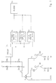
- Fig. 1 shows a schematic overview of three preferred embodiments of the device according to the present invention.
- reference numerals L1 and L2 denote a first and second electrical conductor, which a first and second im lead substantially identical sinusoidal electrical signal, wherein the two signals have a certain phase shift to each other.
- This phase shift is in the range between -180 ° and + 180 ° (- ⁇ and + ⁇ ).
- the device according to the invention serves to determine which sign has the phase shift, ie which of the two signals precedes or follows the other.
- the two electrical conductors have internal or externally inserted resistors 20a, 20b, 20c and 20d and are connected to each other at a common node K, which is at a predetermined potential and is connected via another such resistor 21 to a connection point V.
- connection point V a connection of the common circuit point K to the ground potential PEN can take place via three different types of connection device 11, 12 and 13.
- Reference numeral 11 denotes a connection means for connecting the common node K to the ground potential PEN via a galvanic connection line.
- Reference numeral 12 denotes a connection means for connecting the common node K to the ground potential PEN via a resistive connecting line passing through a touch electrode and the human body 100.
- R and 101 denote a respective resistor and 102 a capacitance.
- Numeral 13 denotes a connection means for connecting the common node K to the ground potential PEN via a capacitive connection line passing through the human body 100.
- C and 102 denote a respective capacitance and 101 a resistor.
- Reference numeral 25 denotes a triggering device for receiving the tapped first signal of the first conductor L1.
- the trigger device sets a temporal reference point and / or a temporal reference window within the signal period of the first signal and outputs a corresponding trigger signal.
- the triggering device 25 generates an arbitrarily definable but constant phase position of the first signal, e.g. certain zero crossing or maximum or minimum or certain slope, a timing pulse.
- This timing pulse is passed to a determination device 31, which detects the polarity of the second signal at the time of the timing pulse and determines therefrom the sign of the phase shift, that is, performs a time analysis.
- the trigger device 25 generates an arbitrarily definable but constant phase position of the first signal, e.g. certain zero crossing or maximum or minimum or certain slope, a time window pulse for the duration of half a signal period of the first signal.
- This time window pulse is passed to a determination device 32, which detects whether the second signal has a predetermined zero crossing during the duration of the time window pulse, and from this determines the sign of the phase shift, that is, performs a time window analysis.
- the trigger device 25 also generates a time window pulse for the duration of half a signal period of the first signal, this one with a certain sign of the first signal coincides.
- This time window pulse is passed to a determination device 33, which is also supplied with the second signal in digitized form.
- This determination device 33 detects whether the second signal has a predetermined edge during the time window pulse, and from this determines the sign of the phase shift, thus carrying out a logic analysis.
- a display 50 e.g. a screen or LCD display.
- Fig. 2 shows a schematic representation of the first preferred embodiment of the device according to the present invention.
- the trigger device has a first comparator 301 for receiving the first signal and comparing it with a predetermined reference potential, preferably earth potential, and a differentiator 41 for differentiating the output signal of the first comparator 301.
- the determining means comprises, in the first embodiment, a second comparator 311 for receiving the second signal and comparing it with the predetermined reference potential, and a memory means 42 for receiving the output of the differentiator 41 at an input E1 and the output of the second comparator 311 at an input E2 ,
- the memory device 42 is designed such that it is at each output pulse of the differentiator 41 with a positive Sign stores the sign of the output signal of the second comparator 311.
- the memory device 42 expediently comprises a flip-flop device for this purpose.
- the memory device 42 has two outputs A1 and A2, which are connected to the display 50.
- the first output A1 activates a "right" display 501, 502 for indicating a rightward shift of the second signal from the first signal, i. a negative sign of the phase shift.
- the second output A2 activates a "left" display 511, 512 for indicating a left shift of the second signal from the first signal, i. a positive sign of the phase shift.
- the display 50 consists in each case of a driver 501, 511 and a luminaire 502, 512 controlled by it.
- FIG. 3 shows diagrams of the phase-shifted signals of the two electrical conductors L1, L2 for explaining the first embodiment according to FIG. 2.
- the time is plotted on the abscissa and the respective signal amplitude is plotted on the ordinate.
- Fig. 3.1 shows the case where the first signal on the first conductor L1 precedes the second signal on the second conductor L2.
- the differentiator 41 outputs a positive pulse each time a rising zero crossing of the first signal, because always then the signal of the comparator 301 changes with rising edge.
- the second signal is always at the time of the positive pulse which is detected by the memory device 42 from the output signal of the second comparator 311, stored and brought via the output A2 to the display 50, in which consequently the left lamp 512 lights up.
- Fig. 3.2 shows the case where the second signal on the second conductor L2 precedes the first signal on the first conductor L1.
- the second signal is always negative at the time of the positive pulse, which is indicated by highlighted points in the waveform of the first signal, which is detected by the memory device 42 from the output of the second comparator 311, stored and via the output A1 is brought to the display 50, in which consequently the right lamp 502 lights up.
- Fig. 4 shows a schematic representation of the second preferred embodiment of the device according to the present invention.
- the triggering means in the second embodiment also has a first comparator 301 for receiving the first signal and comparing it with a predetermined reference potential, preferably ground potential, and a differentiator 41 for differentiating the output signal of the first comparator.
- the trigger means comprises a time window generator 44, suitably a monoflop, for receiving the output signal of the differentiator 41 and generating a time window signal at each output pulse of the differentiator 41 with a positive sign.
- the time window may also be generated in response to an output pulse of the differentiator 41 having a negative sign.
- the determining means in the second embodiment also has a second comparator 311 for receiving the second signal and comparing it with the predetermined reference potential, and memory means 46 for receiving the output of the time-slot generating means 44 at a first input E1 and the output of the second comparator at one second input E2 on.
- the memory device 46 is configured to store the occurrence of a falling zero crossing of the second signal within the temporal reference window.
- the memory device 46 expediently comprises a Schmitt trigger device for this purpose. Of course, it could also store the occurrence of a rising zero crossing.
- FIG. 5 shows diagrams of the phase-shifted signals of the two electrical conductors L1, L2 for explaining the second embodiment according to FIG. 4.
- the time is plotted on the abscissa and the respective signal amplitude is plotted on the ordinate.
- Fig. 5.1 shows the case where the first signal on the first conductor L1 precedes the second signal on the second conductor L2.
- the differentiator 41 each time at a rising zero crossing of the first signal outputs a positive pulse, because always the signal of the comparator 301 changes with rising edge.
- the time-window generator 44 In response thereto, as indicated in FIG. 5.1 by a dashed time window of half the signal period T / 2 of the first signal following the highlighted points, the time-window generator 44 generates a time-window signal with the length T / 2 and applies this to the input E1 of the memory device 46.
- Fig. 5.2 shows the case where the second signal on the second conductor L2 precedes the first signal on the first conductor L1.
- Fig. 6 shows a schematic representation of the third preferred embodiment of the device according to the present invention.
- the trigger means in the third embodiment also has a first comparator 301 for receiving the first signal and comparing it with a predetermined reference potential, preferably ground potential.
- the determining means in the third embodiment has a second comparator 311 for receiving the second signal and comparing it with the predetermined reference potential, and a logic processing means 48 for receiving the output of the first comparator 301 at a first input E1 and the second comparator 311 to a second input E2.
- the logic processing means 48 is arranged to determine the sign of the phase shift by determining whether the second signal has a falling edge when the output of the first comparator 301 goes high.
- the presence of a rising edge can also be detected, and the L state of the output signal of the first comparator 301 can also be used as the trigger signal.
- FIG. 7 shows diagrams of the phase-shifted signals of the two electrical conductors L1, L2 for explaining the second embodiment according to FIG. 6.
- the time is plotted on the abscissa and the respective signal amplitude is plotted on the ordinate.
- Fig. 7.1 shows the case where the first signal on the first conductor L1 precedes the second signal on the second conductor L2.
- X1 denotes the digitized form of the first signal of the first conductor L1 corresponding to the output of the first comparator 301 and X2 the digitized form of the second signal of the second conductor L2 corresponding to the output of the second comparator 311.
- the second digitized signal X2 always has a falling edge during the H state of the first digitized signal X1 due to the positive sign of the phase shift. This is detected by the logic processing device 48, stored and brought to the display 50 via the output A2, whereupon the left lamp 512 lights up.
- Fig. 7.2 shows the case where the second signal on the second conductor L2 precedes the first signal on the first conductor L1.
- the second digitized signal X2 has no falling edge during the H state of the first digitized signal X1 due to the negative sign of the phase shift. This is detected by the logic processing device 48, stored and brought to the display 50 via the output A2, whereupon the right lamp 502 lights up.
- first to third embodiments have been discussed individually, they are of course freely combinable. Also, several consecutive events, i. Measurements in successive signal periods, e.g. averaged. This is particularly important in the case of very noisy signals.
Landscapes
- Physics & Mathematics (AREA)
- General Physics & Mathematics (AREA)
- Measuring Phase Differences (AREA)
- Control Of Eletrric Generators (AREA)
Claims (16)
- Dispositif de détermination du signe d'un décalage de phase entre des premier et deuxième signaux électriques périodiques pour l'essentiel identiques (21, 22) sur un premier et un deuxième conducteur électrique correspondants, en particulier pour la détermination du sens du champ tournant dans un réseau triphasé, comprenant :- un dispositif de détection (20a-20d) pour détecter le premier signal (21) du premier conducteur et le deuxième signal (22) du deuxième conducteur ;- un dispositif de déclenchement (25) pour recevoir le premier signal détecté (21) et déterminer un instant de référence ou un intervalle de temps de référence à l'intérieur de la période de signal du premier signal (21) et émettre un signal de déclenchement correspondant ; et- un dispositif de détermination (31 ; 32 ; 33) pour recevoir le signal de déclenchement et le deuxième signal détecté (22) et déterminer le signe du décalage de phase en prenant en compte au moins la valeur du deuxième signal (22) à l'instant de référence ou le tracé du deuxième signal à l'intérieur de l'intervalle de temps de référence,caractérisé en ce que
le dispositif de déclenchement (25) présente un premier dispositif comparateur (301) pour recevoir le premier signal (21) et le comparer à un potentiel de référence prédéterminé et un dispositif de différenciation (41) pour différencier le signal de sortie du premier dispositif comparateur (301) ; et
le dispositif de détermination (31) présente un deuxième dispositif comparateur (311) pour recevoir le deuxième signal (22) et le comparer au potentiel de référence prédéterminé et un dispositif de mémoire (42) pour recevoir le signal de sortie du deuxième dispositif comparateur (311) et le signal de sortie du dispositif de différenciation (41),
le dispositif de mémoire (42) étant conçu pour qu'à chaque signal de sortie du dispositif de différenciation (41) ayant un signe prédéterminé, il mémorise le signe du signal de sortie du deuxième dispositif comparateur (311). - Dispositif selon la revendication 1,
caractérisé en ce que
le dispositif de mémoire (42) présente un dispositif à bascule bistable. - Dispositif selon la revendication 1,
caractérisé en ce que
le dispositif de déclenchement (25) détermine, en tant qu'intervalle de temps de référence, une demi-période de signal du premier signal (21) suivant un passage au point zéro prédéterminé du premier signal (21). - Dispositif selon la revendication 3,
caractérisé en ce que
le dispositif de détermination (32) détermine le signe du décalage de phase en déterminant si le deuxième signal (22) présente un passage au point zéro prédéterminé à l'intérieur de l'intervalle de temps de référence. - Dispositif de détermination du signe d'un décalage de phase entre des premier et deuxième signaux électriques périodiques pour l'essentiel identiques (21, 22) sur un premier et un deuxième conducteur électrique correspondants, en particulier pour la détermination du sens du champ tournant dans un réseau triphasé, comprenant :- un dispositif de détection (20a-20d) pour détecter le premier signal (21) du premier conducteur et le deuxième signal (22) du deuxième conducteur;- un dispositif de déclenchement (25) pour recevoir le premier signal détecté (21) et déterminer un instant de référence ou un intervalle de temps de référence à l'intérieur de la période de signal du premier signal (21) et émettre un signal de déclenchement correspondant ; et- un dispositif de détermination (31 ; 32 ; 33) pour recevoir le signal de déclenchement et le deuxième signal détecté (22) et déterminer le signe du décalage de phase en prenant en compte au moins la valeur du deuxième signal (22) à l'instant de référence ou le tracé du deuxième signal à l'intérieur de l'intervalle de temps de référence,caractérisé en ce que
le dispositif de déclenchement (25) présente un premier dispositif comparateur (301) pour recevoir le premier signal (21) et le comparer à un potentiel de référence prédéterminé et un dispositif de différenciation (41) pour différencier le signal de sortie du premier dispositif comparateur (301), ainsi qu'un dispositif de génération d'intervalle de temps (44) pour recevoir le signal de sortie du dispositif de différenciation et générer un signal d'intervalle de temps à chaque signal de sortie du dispositif de différenciation (41) ayant un signe prédéterminé ; et
le dispositif de détermination (32) présente un deuxième dispositif comparateur (311) pour recevoir le deuxième signal (22) et le comparer au potentiel de référence prédéterminé et un dispositif de mémoire (46) pour recevoir le signal d'intervalle de temps du dispositif de génération d'intervalle de temps (44) et le signal de sortie du deuxième dispositif comparateur (311),
le dispositif de mémoire (46) étant conçu pour mémoriser l'apparition d'un passage au point zéro prédéterminé du deuxième signal (22) à l'intérieur de l'intervalle de temps de référence. - Dispositif selon la revendication 5,
caractérisé en ce que
le dispositif de mémoire (46) présente un dispositif à bascule de Schmitt. - Dispositif selon la revendication 1,
caractérisé en ce que
le dispositif de déclenchement (25) détermine un demi-seuil prédéterminé du premier signal en tant qu'intervalle de temps de référence. - Dispositif selon la revendication 7,
caractérisé en ce que
le dispositif de détermination (33) numérise et mémorise au moins le deuxième signal (22), et détermine le signe du décalage de phase en déterminant si le deuxième signal numérisé (22) présente une pente prédéterminée à l'intérieur de l'intervalle de temps de référence. - Dispositif de détermination du signe d'un décalage de phase entre des premier et deuxième signaux électriques périodiques pour l'essentiel identiques (21, 22) sur un premier et un deuxième conducteur électrique correspondants, en particulier pour la détermination du sens du champ tournant dans un réseau triphasé, comprenant :- un dispositif de détection (20a-20d) pour détecter le premier signal (21) du premier conducteur et le deuxième signal (22) du deuxième conducteur ;- un dispositif de déclenchement (25) pour recevoir le premier signal détecté (21) et déterminer un instant de référence ou un intervalle de temps de référence à l'intérieur de la période de signal du premier signal (21) et émettre un signal de déclenchement correspondant ; et- un dispositif de détermination (31 ; 32 ; 33) pour recevoir le signal de déclenchement et le deuxième signal détecté (22) et déterminer le signe du décalage de phase en prenant en compte au moins la valeur du deuxième signal (22) à l'instant de référence ou le tracé du deuxième signal à l'intérieur de l'intervalle de temps de référence,caractérisé en ce que
le dispositif de déclenchement (25) présente un premier dispositif comparateur (301) pour recevoir le premier signal (21) et le comparer à un potentiel de référence prédéterminé ; et
le dispositif de détermination (33) présente un deuxième dispositif comparateur (311) pour recevoir le deuxième signal (22) et le comparer au potentiel de référence prédéterminé et un dispositif de traitement logique (48) pour recevoir le signal de sortie du premier dispositif comparateur (301) et du deuxième dispositif comparateur (311),
le dispositif de traitement logique (48) étant conçu pour déterminer le signe du décalage de phase en déterminant si le deuxième signal (22) présente une pente prédéterminée lorsque le signal de sortie du premier dispositif comparateur (301) adopte un état prédéterminé. - Dispositif selon l'une des revendications précédentes,
caractérisé par
un dispositif d'affichage (50) relié au dispositif de détermination (31; 32 ; 33), pour afficher le signe déterminé du décalage de phase. - Dispositif selon l'une des revendications précédentes,
caractérisé en ce que
le dispositif de détection (20a-20d) est conçu pour uniquement des composants résistifs pour la détection du premier (21) et du deuxième (22) signaux. - Dispositif selon l'une des revendications précédentes,
caractérisé en ce que
le premier et le deuxième conducteur électrique sont reliés à un point de circuit commun (K) situé sur un potentiel déterminé. - Dispositif selon la revendication 12,
caractérisé en ce que
le point de circuit commun peut être relié à la masse. - Dispositif selon la revendication 13,
caractérisé par
un dispositif de connexion galvanique (11) pour relier le point de circuit commun à la masse. - Dispositif selon la revendication 13,
caractérisé en ce que
pour relier le point de circuit commun à la masse, un dispositif de connexion résistif (12) est relié à une électrode de contact qui, lorsqu'on la touche, permet la connexion à la masse via le corps de la personne qui la touche. - Dispositif selon la revendication 13,
caractérisé en ce que
pour relier le point de circuit commun à la masse, un dispositif de connexion capacitif (13) est relié à une électrode de contact qui, lorsqu'on la touche, permet la connexion à la masse via le corps de la personne qui la touche.
Applications Claiming Priority (2)
| Application Number | Priority Date | Filing Date | Title |
|---|---|---|---|
| DE19653323A DE19653323C2 (de) | 1996-12-20 | 1996-12-20 | Vorrichtung zur Bestimmung des Vorzeichens einer Phasenverschiebung zweier elektrischer Signale |
| DE19653323 | 1996-12-20 |
Publications (4)
| Publication Number | Publication Date |
|---|---|
| EP0849601A2 EP0849601A2 (fr) | 1998-06-24 |
| EP0849601A3 EP0849601A3 (fr) | 1999-07-28 |
| EP0849601B1 true EP0849601B1 (fr) | 2007-01-10 |
| EP0849601B9 EP0849601B9 (fr) | 2008-04-30 |
Family
ID=7815553
Family Applications (1)
| Application Number | Title | Priority Date | Filing Date |
|---|---|---|---|
| EP97120612A Expired - Lifetime EP0849601B9 (fr) | 1996-12-20 | 1997-11-25 | Appareil et procédé pour déterminer le signe d'un décalage de phase entre deux signaux électriques |
Country Status (5)
| Country | Link |
|---|---|
| US (1) | US6144925A (fr) |
| EP (1) | EP0849601B9 (fr) |
| DE (2) | DE19653323C2 (fr) |
| DK (1) | DK0849601T3 (fr) |
| ES (1) | ES2276415T3 (fr) |
Families Citing this family (7)
| Publication number | Priority date | Publication date | Assignee | Title |
|---|---|---|---|---|
| FI102699B1 (fi) * | 1997-08-27 | 1999-01-29 | Ensto Sekko Oy | Menetelmä ja laite kolmivaihejärjestelmän vaihejärjestyksen ja kiertosuunnan mittaamiseksi |
| DE19915968A1 (de) * | 1999-04-09 | 2000-10-12 | Philips Corp Intellectual Pty | Anordnung zum Offsetabgleich zweier orthogonaler Sensorsignale |
| US6690151B2 (en) * | 2002-03-12 | 2004-02-10 | And Yet, Inc. | Phase detection circuit |
| EP1491904B1 (fr) * | 2003-06-24 | 2007-08-15 | Chauvin Arnoux | Procédé et dispositif d'identification du sens de rotation de deux phases d'un système de tension triphasé |
| DE102006009360B3 (de) * | 2006-03-01 | 2007-07-12 | Wupper, Horst, Prof. Dr. Ing. | Schaltungsanordnung zur elektronischen Bestimmung der Phasenfolge in Drehstromnetzen |
| KR101510653B1 (ko) * | 2007-11-14 | 2015-04-10 | 가부시키가이샤 한도오따이 에네루기 켄큐쇼 | 액정 표시 장치 |
| CN116449122B (zh) * | 2023-06-16 | 2023-08-18 | 创辉科技有限公司 | 供电系统故障检测电路 |
Family Cites Families (13)
| Publication number | Priority date | Publication date | Assignee | Title |
|---|---|---|---|---|
| US3652933A (en) * | 1969-12-23 | 1972-03-28 | Westinghouse Electric Corp | Apparatus for producing a signal when a selected phase relationship exists between two alternating current voltages of different frequencies |
| US4246497A (en) * | 1978-09-29 | 1981-01-20 | Neil Brown Instruments Systems, Inc. | Phase measuring circuit |
| GB2059078A (en) * | 1979-09-13 | 1981-04-15 | Plessey Co Ltd | Improvements in or relating to phase sequence indicators |
| DE3117284A1 (de) * | 1981-04-30 | 1982-11-25 | Siemens AG, 1000 Berlin und 8000 München | Schaltungsanordnung zur ueberwachung eines symmetrischen dreiphasen-wechselstromes |
| US4710703A (en) * | 1986-01-15 | 1987-12-01 | Westinghouse Electric Corp. | Direction sensing system for an AC power supply and AC motor drive with such direction sensing system |
| US4901005A (en) * | 1988-12-05 | 1990-02-13 | International Business Machines Corporation | Zero voltage crossover detector for polyphase systems |
| DE4002603C2 (de) * | 1990-01-30 | 1994-02-03 | Benning Elektrotechnik | Spannungsprüfer |
| US5212407A (en) * | 1990-10-04 | 1993-05-18 | International Business Machines Corporation | Digital phase match discriminator for three-phase power |
| US5103162A (en) * | 1991-03-21 | 1992-04-07 | Westinghouse Electric Corp. | Apparatus for determining when a preselected phase relationship exists between two periodic waveforms |
| DE9206307U1 (de) * | 1992-05-11 | 1992-07-23 | Ch. Beha GmbH Technische Neuentwicklungen, 7804 Glottertal | Drehfeldrichtungs-Meßgerät |
| US5378979A (en) * | 1992-11-25 | 1995-01-03 | Allen-Bradley Company, Inc. | Method and apparatus for efficiently computing symmetric sequence signals in a three phase power system |
| EP0715723B1 (fr) * | 1993-08-23 | 2003-06-11 | Echelon Corporation | Mesure de l'intervalle de temps d'une forme d'onde en salve/sinusoidale |
| DE19631807C1 (de) * | 1996-08-07 | 1997-08-28 | Beha C Gmbh | Verfahren zur Bestimmung der Drehfeldrichtung in einem Dreiphasennetz (Drehstromnetz) |
-
1996
- 1996-12-20 DE DE19653323A patent/DE19653323C2/de not_active Expired - Fee Related
-
1997
- 1997-11-25 EP EP97120612A patent/EP0849601B9/fr not_active Expired - Lifetime
- 1997-11-25 ES ES97120612T patent/ES2276415T3/es not_active Expired - Lifetime
- 1997-11-25 DK DK97120612T patent/DK0849601T3/da active
- 1997-11-25 DE DE59712798T patent/DE59712798D1/de not_active Expired - Lifetime
- 1997-12-18 US US08/993,522 patent/US6144925A/en not_active Expired - Lifetime
Also Published As
| Publication number | Publication date |
|---|---|
| DE19653323C2 (de) | 2001-07-12 |
| DE19653323A1 (de) | 1998-07-02 |
| ES2276415T3 (es) | 2007-06-16 |
| US6144925A (en) | 2000-11-07 |
| DE59712798D1 (de) | 2007-02-22 |
| EP0849601A3 (fr) | 1999-07-28 |
| EP0849601B9 (fr) | 2008-04-30 |
| EP0849601A2 (fr) | 1998-06-24 |
| DK0849601T3 (da) | 2007-05-21 |
Similar Documents
| Publication | Publication Date | Title |
|---|---|---|
| EP2482089B1 (fr) | Procédé et système de localisation d'une erreur sur un câble | |
| CH648934A5 (de) | Verfahren zur messung elektrischer leistung. | |
| WO2018046465A1 (fr) | Procédé et dispositif de mesure pour vérifier un harnais de câbles | |
| EP1070939A2 (fr) | Dispositif et méhode de localisation d'un conducteur métallique | |
| DE69726301T2 (de) | Schaltung zur vervielfachung der auflösung und bestimmung der richtung der lageveränderung | |
| EP0849601B1 (fr) | Appareil et procédé pour déterminer le signe d'un décalage de phase entre deux signaux électriques | |
| EP0497994B1 (fr) | Méthode et circuit pour la surveillance d'une chaîne de mesure d'ions ou d'un potentiel redox | |
| DE69113968T2 (de) | Messbrücke für Referenzspannung für Gerät zur Überwachung und Messung der Isolation eines elektrischen Gleichspannungsnetzes. | |
| DE2545325C3 (de) | Schaltungsanordnung zur Messung des Isolationswiderstandes erdfreier Starkstromschaltungen | |
| DE19538163C1 (de) | Vorrichtung zur Drehzahl- und Drehrichtungserkennung mittels magnetfeldabhängiger Widerstandselemente | |
| DE19631807C1 (de) | Verfahren zur Bestimmung der Drehfeldrichtung in einem Dreiphasennetz (Drehstromnetz) | |
| DE19632457C1 (de) | Schaltungsanordnung zur Überwachung eines Sensors | |
| DE102009032095B4 (de) | Anordnung und Verfahren zur Bestimmung einer Winkelstellung | |
| EP0990162B1 (fr) | Procede de detection du sens de rotation dans des reseaux a courant triphase | |
| DE4224858C2 (de) | Verfahren zur Bestimmung der Prüflingsstörschwelle und Bewertung von EMV-Maßnahmen am Prüfling | |
| EP0185255A1 (fr) | Procédé pour déterminer la polarité de composants électroniques et dispositif mettant en oeuvre ce procédé | |
| DE4424059C1 (de) | Verfahren und Meßanordnung in digitalen Systemen zum Messen von Wechselspannung, Wechselstrom und Phasenwinkel eines Meßsignals | |
| DE29815829U1 (de) | Vorrichtung zur handbetätigten Messung elektrischer Signale | |
| DE102016210982A1 (de) | Kapazitiver Grenzstandschalter | |
| DE102013005178B4 (de) | Impedanz-Scanner | |
| EP0706054B1 (fr) | Comparateur de phase | |
| DE19653460C2 (de) | Verfahren zur sensorlosen Schritterkennung bei Schrittmotoren | |
| DE3817659C2 (fr) | ||
| EP0692099A1 (fr) | Appareil de controle de phases | |
| DE2532356C2 (de) | Einrichtung zur Messung und Grenzwertüberwachung der Phasenbeziehung zwischen Strom und Spannung einer an eine Drehstromleitung angeschlossenen Drehstrommaschine |
Legal Events
| Date | Code | Title | Description |
|---|---|---|---|
| PUAI | Public reference made under article 153(3) epc to a published international application that has entered the european phase |
Free format text: ORIGINAL CODE: 0009012 |
|
| AK | Designated contracting states |
Kind code of ref document: A2 Designated state(s): AT BE CH DE DK ES FI FR GB IT LI NL SE |
|
| AX | Request for extension of the european patent |
Free format text: AL;LT;LV;MK;RO;SI |
|
| PUAL | Search report despatched |
Free format text: ORIGINAL CODE: 0009013 |
|
| AK | Designated contracting states |
Kind code of ref document: A3 Designated state(s): AT BE CH DE DK ES FI FR GB GR IE IT LI LU MC NL PT SE |
|
| AX | Request for extension of the european patent |
Free format text: AL;LT;LV;MK;RO;SI |
|
| 17P | Request for examination filed |
Effective date: 19991221 |
|
| AKX | Designation fees paid |
Free format text: AT BE CH DE DK ES FI FR GB IT LI NL SE |
|
| 17Q | First examination report despatched |
Effective date: 20041022 |
|
| GRAP | Despatch of communication of intention to grant a patent |
Free format text: ORIGINAL CODE: EPIDOSNIGR1 |
|
| RTI1 | Title (correction) |
Free format text: DEVICE AND PROCEDURE FOR DETERMINING THE SIGN OF A PHASE SHIFT BETWEEN TWO ELECTRICAL SIGNALS |
|
| GRAS | Grant fee paid |
Free format text: ORIGINAL CODE: EPIDOSNIGR3 |
|
| GRAA | (expected) grant |
Free format text: ORIGINAL CODE: 0009210 |
|
| AK | Designated contracting states |
Kind code of ref document: B1 Designated state(s): AT BE CH DE DK ES FI FR GB IT LI NL SE |
|
| REG | Reference to a national code |
Ref country code: GB Ref legal event code: FG4D Free format text: NOT ENGLISH |
|
| GBT | Gb: translation of ep patent filed (gb section 77(6)(a)/1977) |
Effective date: 20070110 |
|
| REF | Corresponds to: |
Ref document number: 59712798 Country of ref document: DE Date of ref document: 20070222 Kind code of ref document: P |
|
| REG | Reference to a national code |
Ref country code: SE Ref legal event code: TRGR |
|
| REG | Reference to a national code |
Ref country code: CH Ref legal event code: NV Representative=s name: R. A. EGLI & CO. PATENTANWAELTE |
|
| REG | Reference to a national code |
Ref country code: DK Ref legal event code: T3 |
|
| REG | Reference to a national code |
Ref country code: ES Ref legal event code: FG2A Ref document number: 2276415 Country of ref document: ES Kind code of ref document: T3 |
|
| ET | Fr: translation filed | ||
| PLBE | No opposition filed within time limit |
Free format text: ORIGINAL CODE: 0009261 |
|
| STAA | Information on the status of an ep patent application or granted ep patent |
Free format text: STATUS: NO OPPOSITION FILED WITHIN TIME LIMIT |
|
| 26N | No opposition filed |
Effective date: 20071011 |
|
| PGFP | Annual fee paid to national office [announced via postgrant information from national office to epo] |
Ref country code: DK Payment date: 20141124 Year of fee payment: 18 |
|
| PGFP | Annual fee paid to national office [announced via postgrant information from national office to epo] |
Ref country code: SE Payment date: 20141120 Year of fee payment: 18 Ref country code: CH Payment date: 20141120 Year of fee payment: 18 Ref country code: GB Payment date: 20141120 Year of fee payment: 18 Ref country code: ES Payment date: 20141120 Year of fee payment: 18 Ref country code: FI Payment date: 20141119 Year of fee payment: 18 |
|
| PGFP | Annual fee paid to national office [announced via postgrant information from national office to epo] |
Ref country code: AT Payment date: 20141119 Year of fee payment: 18 Ref country code: FR Payment date: 20141118 Year of fee payment: 18 Ref country code: NL Payment date: 20141120 Year of fee payment: 18 |
|
| PGFP | Annual fee paid to national office [announced via postgrant information from national office to epo] |
Ref country code: IT Payment date: 20141125 Year of fee payment: 18 |
|
| PGFP | Annual fee paid to national office [announced via postgrant information from national office to epo] |
Ref country code: BE Payment date: 20141125 Year of fee payment: 18 Ref country code: DE Payment date: 20141218 Year of fee payment: 18 |
|
| REG | Reference to a national code |
Ref country code: DE Ref legal event code: R119 Ref document number: 59712798 Country of ref document: DE |
|
| REG | Reference to a national code |
Ref country code: DK Ref legal event code: EBP Effective date: 20151130 |
|
| REG | Reference to a national code |
Ref country code: CH Ref legal event code: PL |
|
| REG | Reference to a national code |
Ref country code: AT Ref legal event code: MM01 Ref document number: 351368 Country of ref document: AT Kind code of ref document: T Effective date: 20151125 |
|
| GBPC | Gb: european patent ceased through non-payment of renewal fee |
Effective date: 20151125 |
|
| PG25 | Lapsed in a contracting state [announced via postgrant information from national office to epo] |
Ref country code: CH Free format text: LAPSE BECAUSE OF NON-PAYMENT OF DUE FEES Effective date: 20151130 Ref country code: IT Free format text: LAPSE BECAUSE OF NON-PAYMENT OF DUE FEES Effective date: 20151125 Ref country code: LI Free format text: LAPSE BECAUSE OF NON-PAYMENT OF DUE FEES Effective date: 20151130 |
|
| REG | Reference to a national code |
Ref country code: NL Ref legal event code: MM Effective date: 20151201 |
|
| REG | Reference to a national code |
Ref country code: FR Ref legal event code: ST Effective date: 20160729 |
|
| PG25 | Lapsed in a contracting state [announced via postgrant information from national office to epo] |
Ref country code: AT Free format text: LAPSE BECAUSE OF NON-PAYMENT OF DUE FEES Effective date: 20151125 Ref country code: SE Free format text: LAPSE BECAUSE OF NON-PAYMENT OF DUE FEES Effective date: 20151126 |
|
| PG25 | Lapsed in a contracting state [announced via postgrant information from national office to epo] |
Ref country code: NL Free format text: LAPSE BECAUSE OF NON-PAYMENT OF DUE FEES Effective date: 20151201 |
|
| PG25 | Lapsed in a contracting state [announced via postgrant information from national office to epo] |
Ref country code: DE Free format text: LAPSE BECAUSE OF NON-PAYMENT OF DUE FEES Effective date: 20160601 Ref country code: DK Free format text: LAPSE BECAUSE OF NON-PAYMENT OF DUE FEES Effective date: 20151130 Ref country code: GB Free format text: LAPSE BECAUSE OF NON-PAYMENT OF DUE FEES Effective date: 20151125 |
|
| PG25 | Lapsed in a contracting state [announced via postgrant information from national office to epo] |
Ref country code: FR Free format text: LAPSE BECAUSE OF NON-PAYMENT OF DUE FEES Effective date: 20151130 |
|
| REG | Reference to a national code |
Ref country code: ES Ref legal event code: FD2A Effective date: 20161228 |
|
| PG25 | Lapsed in a contracting state [announced via postgrant information from national office to epo] |
Ref country code: ES Free format text: LAPSE BECAUSE OF NON-PAYMENT OF DUE FEES Effective date: 20151126 |
|
| PG25 | Lapsed in a contracting state [announced via postgrant information from national office to epo] |
Ref country code: BE Free format text: LAPSE BECAUSE OF NON-PAYMENT OF DUE FEES Effective date: 20151130 Ref country code: FI Free format text: LAPSE BECAUSE OF NON-PAYMENT OF DUE FEES Effective date: 20151125 |