EP0849738A2 - Améliorations à ou relatives à des systèmes électroniques - Google Patents
Améliorations à ou relatives à des systèmes électroniques Download PDFInfo
- Publication number
- EP0849738A2 EP0849738A2 EP97310338A EP97310338A EP0849738A2 EP 0849738 A2 EP0849738 A2 EP 0849738A2 EP 97310338 A EP97310338 A EP 97310338A EP 97310338 A EP97310338 A EP 97310338A EP 0849738 A2 EP0849738 A2 EP 0849738A2
- Authority
- EP
- European Patent Office
- Prior art keywords
- board
- memory module
- interface
- memory
- operable
- Prior art date
- Legal status (The legal status is an assumption and is not a legal conclusion. Google has not performed a legal analysis and makes no representation as to the accuracy of the status listed.)
- Ceased
Links
Images

Classifications
-
- G—PHYSICS
- G06—COMPUTING OR CALCULATING; COUNTING
- G06F—ELECTRIC DIGITAL DATA PROCESSING
- G06F12/00—Accessing, addressing or allocating within memory systems or architectures
- G06F12/02—Addressing or allocation; Relocation
-
- H—ELECTRICITY
- H10—SEMICONDUCTOR DEVICES; ELECTRIC SOLID-STATE DEVICES NOT OTHERWISE PROVIDED FOR
- H10W—GENERIC PACKAGES, INTERCONNECTIONS, CONNECTORS OR OTHER CONSTRUCTIONAL DETAILS OF DEVICES COVERED BY CLASS H10
- H10W90/00—Package configurations
Definitions
- This invention relates in general to the field of electronic systems, and more particularly to a memory module for high speed and high density systems.
- Computer and other electronic systems have increasingly large demands for system memory. This is especially true for high performance processors and parallel processing system architectures. Electronic systems are contemplated to include in excess of several gigabytes of main memory, such as DRAM memory, to support their processors and software applications. Providing the required memory space for such systems creates problems with addressing speed, density, power dissipation, power distribution, interconnection, interface and physical space. Some conventional methods for addressing problems produced by large memory space include RAMBUS, which is a single bus architecture providing communication between large numbers of memory devices. However, the RAMBUS scheme is limited in bandwidth and has a high overhead which renders RAMBUS unable to use the peak available bus data transfer rate.
- a memory module for high speed and high density systems is provided that substantially reduces or eliminates problems and disadvantages of prior memory modules.
- a memory module that has an outer shield forming an outer perimeter of the memory module.
- a board is positioned inside the outer shield and is coextensive with the outer shield to define an outer portion and an inner portion of the memory module.
- a plurality of memory devices are connected to the board and are positioned in the outer portion between the outer shield and the board. The board is operable to communicate information to and from the memory devices.
- An interface connection is positioned in the inner portion and is operable to communicate information to and from the memory module.
- a first interface driver is connected between the interface connection and the board to communicate information from the interface connection to the board.
- a second interface driver is connected between the interface connection and the board to communicate information from the board to the interface connection.
- a power distribution strip is positioned in the inner portion and connected to the board to provide power to the board. According to one aspect of the present invention, a plurality of these memory modules can be stacked to form a memory tower.
- a technical advantage of the present invention is the provision of a memory module subsystem that supplies data at high bandwidth needed by high performance systems with low physical latency.
- FIGURE 1 is a block diagram of a memory module, indicated generally at 10.
- Memory module 10 includes an outer shield 12 and a flex board 14 which form a container for a plurality of memory devices 16. Outer shield 12 can also form a boundary for a cooling container in which air or fluid is passed between memory devices 16.
- a plurality of memory devices 16 are connected to flex board 14 which is in turn connected to an interface (I/F) driver 18 and an interface driver 20.
- Interface driver 18 and interface driver 20 are connected to an interface connection 22.
- interface connection 22 comprises an optical fiber for carrying information to and from memory module 10.
- Interface driver 18 operates to communicate information from interface connection 22 to flex board 14 and to appropriate memory devices 16.
- interface driver 20 operates to communicate information from memory devices 16 through flex board 14 and to interface connection 22.
- Memory module 10 further includes power distribution strips 24 which provide power to flex board 14.
- memory module 10 provides an interface to memory devices 16 through flex board 14, interface driver 18, interface driver 20 and interface connection 22.
- the distribution of signals and clocks to the various memory devices 16 can utilize a phase locked loop or other suitable synchronization scheme.
- the memory devices are mounted around an interface driver using a flexible optical cable.
- the base shift between the memory devices can be less than around 400 picoseconds, so no need for clock or data shifts exist.
- a phase locked loop clock distribution can be used.
- the data for example, can be multiplexed at the interface driver.
- GaAs gallium arsenic
- SCI small computer interface
- the memory modules can then be stacked in a tower, as shown in FIGURE 4, similar to three-dimensional packaging concepts. These stacks can be a number of memory modules deep.
- the memory modules can be mounted, for example, end-to-end with the last memory module in a tower having a terminator where the terminator simply redirects the optical path through a second fiber passing through the memory modules.
- the memory modules can have laminated flat power buses along the interior of the memory module that also act as part of the power dissipation surface.
- the memory towers can also be enclosed to facilitate forced air or liquid cooling.
- the memory towers may be coupled together either in series or in parallel with a single or separate controller.
- FIGURE 2 is a block diagram of another embodiment of a memory module, indicated generally at 26.
- memory module 26 is similar to that of FIGURE 1 and includes outer shield 12, flex board 14, and a plurality of memory devices 16.
- Memory module 26 also includes interface driver 18, interface driver 20 and interface connections 22.
- memory module 26 includes power distribution strips 24. These pieces operate to provide access to memory devices 16 in the same manner as the embodiment of FIGURE 1.
- the difference between memory module 26 at FIGURE 2 and memory module 10 at FIGURE 1 is that memory module 26 has a larger number of memory devices 16. It should be understood, however, that memory modules can be constructed that have varied numbers of memory devices 16 as are suitable for the desired application.
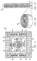
- FIGURE 3 is a block diagram of a further embodiment of a memory module, indicated generally at 30.
- Memory module 30 has a substantially square shape which, in some circumstances, can be produced at lower cost than the circular shapes shown in FIGURE 1 and FIGURE 2.
- Memory module 30 includes an outer shield 32 which, in part, defines a plurality of cooling regions at the corners of the memory module 30.
- a board 36 defines an inner surface to which a plurality of memory devices 38 are connected. Similar to the embodiments described above, air or other fluids can be passed between memory devices 38 and through cooling regions 34 in order to dissipate heat within the structure.
- An interface driver 40 and an interface driver 42 are connected to board 36 and are also connected to an interface connection 44. It is preferred that interface connection 44 comprises an optical fiber for communicating information to and from memory module 30.
- Interface driver 40 provides communication of information from interface connection 44 to board 36 and to appropriate memory devices 38.
- Interface driver 42 provides communication of information from memory devices 38 and memory board 36 to interface connection 44.
- Memory module 30 further includes power distribution strips
- FIGURES 4A and 4B show a block diagram of an embodiment of a tower assembly of memory modules, indicated generally at 50.
- Memory tower assembly 50 includes a plurality of separate memory modules 52 stacked upon and connected to each other. Each memory module 52 is constructed having a unidirectional internal memory communication interface with optical fiber. The optical fiber then runs through all of memory modules 52 and is terminated by returning the signal back down through memory modules 52. Memory modules 52 then communicate along a memory bus with remaining portions of the computer system.
- This memory tower module assembly 50 allows a relatively small physical area to contain a large amount of main memory. For example an area of 22 inches by 22 inches by 4 inches could contain 512 gigabytes of main memory.
Landscapes
- Engineering & Computer Science (AREA)
- Theoretical Computer Science (AREA)
- Physics & Mathematics (AREA)
- General Engineering & Computer Science (AREA)
- General Physics & Mathematics (AREA)
- Shielding Devices Or Components To Electric Or Magnetic Fields (AREA)
- Semiconductor Memories (AREA)
- Memory System (AREA)
Applications Claiming Priority (2)
| Application Number | Priority Date | Filing Date | Title |
|---|---|---|---|
| US3351096P | 1996-12-19 | 1996-12-19 | |
| US33510P | 1996-12-19 |
Publications (2)
| Publication Number | Publication Date |
|---|---|
| EP0849738A2 true EP0849738A2 (fr) | 1998-06-24 |
| EP0849738A3 EP0849738A3 (fr) | 1999-04-21 |
Family
ID=21870811
Family Applications (1)
| Application Number | Title | Priority Date | Filing Date |
|---|---|---|---|
| EP97310338A Ceased EP0849738A3 (fr) | 1996-12-19 | 1997-12-19 | Améliorations à ou relatives à des systèmes électroniques |
Country Status (4)
| Country | Link |
|---|---|
| EP (1) | EP0849738A3 (fr) |
| JP (1) | JPH10247380A (fr) |
| KR (1) | KR19980064369A (fr) |
| TW (1) | TW386199B (fr) |
Cited By (2)
| Publication number | Priority date | Publication date | Assignee | Title |
|---|---|---|---|---|
| DE102006000715B4 (de) * | 2005-01-06 | 2008-07-03 | Samsung Electronics Co., Ltd., Suwon | Speichersystem |
| GB2503807B (en) * | 2012-07-06 | 2015-07-08 | Nvidia Corp | Alternative 3D stacking scheme for DRAMs atop GPUs |
Family Cites Families (2)
| Publication number | Priority date | Publication date | Assignee | Title |
|---|---|---|---|---|
| US3908155A (en) * | 1974-04-19 | 1975-09-23 | Ibm | Wafer circuit package |
| KR960012649B1 (en) * | 1987-04-22 | 1996-09-23 | Hitachi Ltd | Wafer scale or full wafer memory system, package, method thereof and wafer processing method employed therein |
-
1997
- 1997-12-19 KR KR1019970070642A patent/KR19980064369A/ko not_active Withdrawn
- 1997-12-19 EP EP97310338A patent/EP0849738A3/fr not_active Ceased
- 1997-12-19 JP JP9351068A patent/JPH10247380A/ja active Pending
-
1998
- 1998-02-09 TW TW086119244A patent/TW386199B/zh not_active IP Right Cessation
Cited By (4)
| Publication number | Priority date | Publication date | Assignee | Title |
|---|---|---|---|---|
| DE102006000715B4 (de) * | 2005-01-06 | 2008-07-03 | Samsung Electronics Co., Ltd., Suwon | Speichersystem |
| US7583509B2 (en) | 2005-01-06 | 2009-09-01 | Samsung Electronics Co., Ltd. | Memory module and memory system having the same |
| GB2503807B (en) * | 2012-07-06 | 2015-07-08 | Nvidia Corp | Alternative 3D stacking scheme for DRAMs atop GPUs |
| US9343449B2 (en) | 2012-07-06 | 2016-05-17 | Nvidia Corporation | Alternative 3D stacking scheme for DRAMs atop GPUs |
Also Published As
| Publication number | Publication date |
|---|---|
| EP0849738A3 (fr) | 1999-04-21 |
| JPH10247380A (ja) | 1998-09-14 |
| KR19980064369A (ko) | 1998-10-07 |
| TW386199B (en) | 2000-04-01 |
Similar Documents
| Publication | Publication Date | Title |
|---|---|---|
| US5150279A (en) | High performance computer system with platters and unidirectional storage modules therebetween | |
| US5699853A (en) | Combined heat sink and sink plate | |
| US5986882A (en) | Electronic apparatus having removable processor/heat pipe cooling device modules therein | |
| KR101089445B1 (ko) | 스택 외부 측 상에 고전력 칩을 갖는 칩 스택 | |
| US6466441B1 (en) | Cooling device of electronic part having high and low heat generating elements | |
| US5317477A (en) | High density interconnection assembly | |
| US5049982A (en) | Article comprising a stacked array of electronic subassemblies | |
| US20060050496A1 (en) | Thin module system and method | |
| CA1319204C (fr) | Module universel de circuits integres | |
| US6504743B2 (en) | Die architecture accommodating high-speed semiconductor devices | |
| EP4294138A1 (fr) | Unité de commande électronique | |
| KR20150016605A (ko) | 칩 간 메모리 인터페이스 구조 | |
| US20020184328A1 (en) | Chip multiprocessor with multiple operating systems | |
| EP0849738A2 (fr) | Améliorations à ou relatives à des systèmes électroniques | |
| EP4626142A1 (fr) | Ensemble carte de circuit imprimé, module informatique central et véhicule | |
| US4955131A (en) | Method of building a variety of complex high performance IC devices | |
| US12443248B2 (en) | Graphics card expansion device and mobile terminal | |
| US20040109283A1 (en) | Integrated circuit chip package with formable intermediate 3D wiring structure | |
| EP0849168A1 (fr) | Méthode pour ajuster la rigidité et les propriétés acoustiques d'un module d'équipement d'engine spatial permettant un assemblage externe | |
| US11310941B2 (en) | Electronic device and heat sink | |
| US10068886B2 (en) | Implementing inverted master-slave 3D semiconductor stack | |
| CN210112376U (zh) | 一种电路板及电子设备 | |
| JP2776551B2 (ja) | バスライン方式半導体記憶装置 | |
| EP0506224A2 (fr) | Boîtier de système d'ordinateur | |
| US12422903B2 (en) | Independent graphics card system, computer host and computer |
Legal Events
| Date | Code | Title | Description |
|---|---|---|---|
| PUAI | Public reference made under article 153(3) epc to a published international application that has entered the european phase |
Free format text: ORIGINAL CODE: 0009012 |
|
| AK | Designated contracting states |
Kind code of ref document: A2 Designated state(s): DE FR GB IT NL |
|
| AX | Request for extension of the european patent |
Free format text: AL;LT;LV;MK;RO;SI |
|
| PUAL | Search report despatched |
Free format text: ORIGINAL CODE: 0009013 |
|
| AK | Designated contracting states |
Kind code of ref document: A3 Designated state(s): AT BE CH DE DK ES FI FR GB GR IE IT LI LU MC NL PT SE |
|
| 17P | Request for examination filed |
Effective date: 19990929 |
|
| AKX | Designation fees paid |
Free format text: DE FR GB IT NL |
|
| GRAG | Despatch of communication of intention to grant |
Free format text: ORIGINAL CODE: EPIDOS AGRA |
|
| 17Q | First examination report despatched |
Effective date: 20020517 |
|
| STAA | Information on the status of an ep patent application or granted ep patent |
Free format text: STATUS: THE APPLICATION HAS BEEN REFUSED |
|
| 18R | Application refused |
Effective date: 20021121 |