EP0849784A2 - System zum Verbinden eines Leiterrahmens mit einer Halbleitervorrichtung und Trägermechanismus für das Bonden des Leiterrahmens - Google Patents
System zum Verbinden eines Leiterrahmens mit einer Halbleitervorrichtung und Trägermechanismus für das Bonden des Leiterrahmens Download PDFInfo
- Publication number
- EP0849784A2 EP0849784A2 EP97310291A EP97310291A EP0849784A2 EP 0849784 A2 EP0849784 A2 EP 0849784A2 EP 97310291 A EP97310291 A EP 97310291A EP 97310291 A EP97310291 A EP 97310291A EP 0849784 A2 EP0849784 A2 EP 0849784A2
- Authority
- EP
- European Patent Office
- Prior art keywords
- lead
- bonding
- support mechanism
- leads
- leadframe
- Prior art date
- Legal status (The legal status is an assumption and is not a legal conclusion. Google has not performed a legal analysis and makes no representation as to the accuracy of the status listed.)
- Withdrawn
Links
Images



Classifications
-
- H—ELECTRICITY
- H10—SEMICONDUCTOR DEVICES; ELECTRIC SOLID-STATE DEVICES NOT OTHERWISE PROVIDED FOR
- H10W—GENERIC PACKAGES, INTERCONNECTIONS, CONNECTORS OR OTHER CONSTRUCTIONAL DETAILS OF DEVICES COVERED BY CLASS H10
- H10W72/00—Interconnections or connectors in packages
- H10W72/071—Connecting or disconnecting
- H10W72/075—Connecting or disconnecting of bond wires
-
- B—PERFORMING OPERATIONS; TRANSPORTING
- B23—MACHINE TOOLS; METAL-WORKING NOT OTHERWISE PROVIDED FOR
- B23K—SOLDERING OR UNSOLDERING; WELDING; CLADDING OR PLATING BY SOLDERING OR WELDING; CUTTING BY APPLYING HEAT LOCALLY, e.g. FLAME CUTTING; WORKING BY LASER BEAM
- B23K20/00—Non-electric welding by applying impact or other pressure, with or without the application of heat, e.g. cladding or plating
- B23K20/002—Non-electric welding by applying impact or other pressure, with or without the application of heat, e.g. cladding or plating specially adapted for particular articles or work
-
- H—ELECTRICITY
- H10—SEMICONDUCTOR DEVICES; ELECTRIC SOLID-STATE DEVICES NOT OTHERWISE PROVIDED FOR
- H10W—GENERIC PACKAGES, INTERCONNECTIONS, CONNECTORS OR OTHER CONSTRUCTIONAL DETAILS OF DEVICES COVERED BY CLASS H10
- H10W70/00—Package substrates; Interposers; Redistribution layers [RDL]
- H10W70/40—Leadframes
- H10W70/421—Shapes or dispositions
- H10W70/424—Cross-sectional shapes
- H10W70/427—Bent parts
-
- H—ELECTRICITY
- H10—SEMICONDUCTOR DEVICES; ELECTRIC SOLID-STATE DEVICES NOT OTHERWISE PROVIDED FOR
- H10W—GENERIC PACKAGES, INTERCONNECTIONS, CONNECTORS OR OTHER CONSTRUCTIONAL DETAILS OF DEVICES COVERED BY CLASS H10
- H10W70/00—Package substrates; Interposers; Redistribution layers [RDL]
- H10W70/40—Leadframes
- H10W70/421—Shapes or dispositions
- H10W70/435—Shapes or dispositions of insulating layers on leadframes, e.g. bridging members
-
- H—ELECTRICITY
- H10—SEMICONDUCTOR DEVICES; ELECTRIC SOLID-STATE DEVICES NOT OTHERWISE PROVIDED FOR
- H10W—GENERIC PACKAGES, INTERCONNECTIONS, CONNECTORS OR OTHER CONSTRUCTIONAL DETAILS OF DEVICES COVERED BY CLASS H10
- H10W72/00—Interconnections or connectors in packages
- H10W72/50—Bond wires
-
- B—PERFORMING OPERATIONS; TRANSPORTING
- B23—MACHINE TOOLS; METAL-WORKING NOT OTHERWISE PROVIDED FOR
- B23K—SOLDERING OR UNSOLDERING; WELDING; CLADDING OR PLATING BY SOLDERING OR WELDING; CUTTING BY APPLYING HEAT LOCALLY, e.g. FLAME CUTTING; WORKING BY LASER BEAM
- B23K2101/00—Articles made by soldering, welding or cutting
- B23K2101/36—Electric or electronic devices
- B23K2101/40—Semiconductor devices
-
- H—ELECTRICITY
- H10—SEMICONDUCTOR DEVICES; ELECTRIC SOLID-STATE DEVICES NOT OTHERWISE PROVIDED FOR
- H10W—GENERIC PACKAGES, INTERCONNECTIONS, CONNECTORS OR OTHER CONSTRUCTIONAL DETAILS OF DEVICES COVERED BY CLASS H10
- H10W70/00—Package substrates; Interposers; Redistribution layers [RDL]
- H10W70/60—Insulating or insulated package substrates; Interposers; Redistribution layers
- H10W70/67—Insulating or insulated package substrates; Interposers; Redistribution layers characterised by their insulating layers or insulating parts
- H10W70/68—Shapes or dispositions thereof
- H10W70/682—Shapes or dispositions thereof comprising holes having chips therein
-
- H—ELECTRICITY
- H10—SEMICONDUCTOR DEVICES; ELECTRIC SOLID-STATE DEVICES NOT OTHERWISE PROVIDED FOR
- H10W—GENERIC PACKAGES, INTERCONNECTIONS, CONNECTORS OR OTHER CONSTRUCTIONAL DETAILS OF DEVICES COVERED BY CLASS H10
- H10W72/00—Interconnections or connectors in packages
- H10W72/071—Connecting or disconnecting
- H10W72/075—Connecting or disconnecting of bond wires
- H10W72/07531—Techniques
- H10W72/07532—Compression bonding, e.g. thermocompression bonding
-
- H—ELECTRICITY
- H10—SEMICONDUCTOR DEVICES; ELECTRIC SOLID-STATE DEVICES NOT OTHERWISE PROVIDED FOR
- H10W—GENERIC PACKAGES, INTERCONNECTIONS, CONNECTORS OR OTHER CONSTRUCTIONAL DETAILS OF DEVICES COVERED BY CLASS H10
- H10W72/00—Interconnections or connectors in packages
- H10W72/071—Connecting or disconnecting
- H10W72/075—Connecting or disconnecting of bond wires
- H10W72/07551—Connecting or disconnecting of bond wires characterised by changes in properties of the bond wires during the connecting
- H10W72/07554—Connecting or disconnecting of bond wires characterised by changes in properties of the bond wires during the connecting changes in dispositions
-
- H—ELECTRICITY
- H10—SEMICONDUCTOR DEVICES; ELECTRIC SOLID-STATE DEVICES NOT OTHERWISE PROVIDED FOR
- H10W—GENERIC PACKAGES, INTERCONNECTIONS, CONNECTORS OR OTHER CONSTRUCTIONAL DETAILS OF DEVICES COVERED BY CLASS H10
- H10W72/00—Interconnections or connectors in packages
- H10W72/50—Bond wires
- H10W72/531—Shapes of wire connectors
- H10W72/536—Shapes of wire connectors the connected ends being ball-shaped
-
- H—ELECTRICITY
- H10—SEMICONDUCTOR DEVICES; ELECTRIC SOLID-STATE DEVICES NOT OTHERWISE PROVIDED FOR
- H10W—GENERIC PACKAGES, INTERCONNECTIONS, CONNECTORS OR OTHER CONSTRUCTIONAL DETAILS OF DEVICES COVERED BY CLASS H10
- H10W72/00—Interconnections or connectors in packages
- H10W72/50—Bond wires
- H10W72/531—Shapes of wire connectors
- H10W72/5363—Shapes of wire connectors the connected ends being wedge-shaped
-
- H—ELECTRICITY
- H10—SEMICONDUCTOR DEVICES; ELECTRIC SOLID-STATE DEVICES NOT OTHERWISE PROVIDED FOR
- H10W—GENERIC PACKAGES, INTERCONNECTIONS, CONNECTORS OR OTHER CONSTRUCTIONAL DETAILS OF DEVICES COVERED BY CLASS H10
- H10W72/00—Interconnections or connectors in packages
- H10W72/50—Bond wires
- H10W72/541—Dispositions of bond wires
- H10W72/5449—Dispositions of bond wires not being orthogonal to a side surface of the chip, e.g. fan-out arrangements
-
- H—ELECTRICITY
- H10—SEMICONDUCTOR DEVICES; ELECTRIC SOLID-STATE DEVICES NOT OTHERWISE PROVIDED FOR
- H10W—GENERIC PACKAGES, INTERCONNECTIONS, CONNECTORS OR OTHER CONSTRUCTIONAL DETAILS OF DEVICES COVERED BY CLASS H10
- H10W72/00—Interconnections or connectors in packages
- H10W72/50—Bond wires
- H10W72/541—Dispositions of bond wires
- H10W72/547—Dispositions of multiple bond wires
-
- H—ELECTRICITY
- H10—SEMICONDUCTOR DEVICES; ELECTRIC SOLID-STATE DEVICES NOT OTHERWISE PROVIDED FOR
- H10W—GENERIC PACKAGES, INTERCONNECTIONS, CONNECTORS OR OTHER CONSTRUCTIONAL DETAILS OF DEVICES COVERED BY CLASS H10
- H10W72/00—Interconnections or connectors in packages
- H10W72/90—Bond pads, in general
- H10W72/931—Shapes of bond pads
- H10W72/932—Plan-view shape, i.e. in top view
-
- H—ELECTRICITY
- H10—SEMICONDUCTOR DEVICES; ELECTRIC SOLID-STATE DEVICES NOT OTHERWISE PROVIDED FOR
- H10W—GENERIC PACKAGES, INTERCONNECTIONS, CONNECTORS OR OTHER CONSTRUCTIONAL DETAILS OF DEVICES COVERED BY CLASS H10
- H10W90/00—Package configurations
- H10W90/701—Package configurations characterised by the relative positions of pads or connectors relative to package parts
- H10W90/751—Package configurations characterised by the relative positions of pads or connectors relative to package parts of bond wires
- H10W90/756—Package configurations characterised by the relative positions of pads or connectors relative to package parts of bond wires between a chip and a stacked lead frame, conducting package substrate or heat sink
Definitions
- This invention relates generally to the field of integrated circuits, and more particularly to a system, apparatus, and method for connecting a semiconductor chip to a three-dimensional leadframe.
- a leadframe may be electrically coupled to an integrated circuit during the fabrication of an electronic component.
- Methods for coupling the leadframe to the integrated circuit include wire bonding such as ball bonding or wedge bonding.
- the leadframe, integrated circuit, and bond wire may be encapsulated by a plastic molding process to form a package.
- Bonding with bonding wire entails securing a bonding wire between a contact or a bond pad on an integrated circuit and a bonding site or target on a lead tip of a lead or lead finger on a leadframe. As the distances between bond pads on integrated circuits are reduced, the size of the integrated circuit die can be reduced while producing substantially equal performance and using less silicon.
- Three-dimensional leads have also been utilized in an effort to minimize wire crossing and shorting during the fill process of packaging a semiconductor chip.
- United States Patent 5,530,281 entitled Wire Bond Lead System with Improved Wire Separation, discloses a leadframe with three-dimensional leads for this purpose.
- the '281 Patent does not, however, disclose an efficient method for making leads or for bonding to such leads.
- a heating block may be used.
- United States Patent 5,558,267 entitled Moat For Die Pad Cavity in Bond Station Heater Block, shows, a heating block to assist with bonding.
- the heating block may be heated by a heater as is known in the art.
- a system, apparatus and method for connecting a semiconductor chip to a leadframe are provided that address the shortcomings of prior devices and techniques.
- the system for connecting a semiconductor chip to a leadframe may include a three-dimensional leadframe and a bonding support mechanism having a trough.
- the leadframe may have a first lead having a first base portion, a first lead tip, and a first longitudinal axis, a second lead having a second base portion, a second lead tip, and a second longitudinal axis, the first and second leads formed substantially adjacent to each other, and the second lead having a stepped portion such that the lead tips of the first and second leads are separated in a Z-direction and in a Y-direction (where the Y-direction is parallel to the longitudinal axis of the leads and an X-direction intersects adjacent leads) .
- the bonding support mechanism may include a support body, with the trough formed on the support body, and the trough having a first surface at a first elevation, the first surface for supporting the second lead tip, and the bonding support mechanism may include a second surface, which is for supporting the first lead tip formed on the support body at a second elevation and substantially adjacent to the first surface.
- a bonding support mechanism may have an angled surface to accommodate a stepped portion of a downset lead of a leadframe.
- a method for connecting a semiconductor chip to a leadframe may include the steps of forming a three-dimensional leadframe with a first lead having a first base portion, a first lead tip, and a first longitudinal axis; forming a second lead having a second base portion, a second lead tip, and a second longitudinal axis, and with the first and second leads formed substantially adjacent to each other; forming a stepped portion on the second lead; and bonding lead wires to the plurality of leads by placing the first lead tip of the first lead on a first surface of a ridge of a bonding support mechanism and placing the second lead tip of the second lead on a second surface formed as part of a trough of a bonding support mechanism, and applying bonding wires between the chip and the first lead tip and second lead tip.
- a technical advantage of the present invention is that three-dimensional leads may be efficiently manufactured and bonded to a semiconductor chip. Another technical advantage is that the trough of the bonding support mechanism facilitates positioning of the leads with respect to the bonding support mechanism. Another technical advantage is that a bonding support mechanism is provided that is relatively easy to manufacture.
- FIGURES 1 through 9 of the drawings like numerals being used for like and corresponding parts of the various drawings.
- Leadframe 12 has a number of basic leadframe features 14 including leads 16, which will allow the final package to be electrically coupled to electronic systems.
- Leadframe 12 is formed with a plurality of leads 18.
- Die pad 20 is supported by a plurality of securing leads or straps 24.
- Semiconductor chip 22 has a plurality of bonding pads 26 on a surface.
- Bond pads 26 may be electrically coupled to leadframe 12 by the application of bonding wires 28 between the plurality of leads 18 and the bonding pads 26.
- the connections involving bonding wire 28 may be made by any of a number of techniques such as ball bonding or wedge bonding.
- the leads 18 are supported during bonding by a bonding support mechanism as will be described in connection with FIGURES 6-9.
- FIGURE 2 a perspective view of a portion of leadframe 12 is shown, and in particular, three leads from the plurality of leads 18 (FIGURE 1) are shown. Three leads are shown for illustration purposes, but it is to be understood that the description of the three leads may apply analogously to all of the plurality of leads 18.
- a first lead 30, second lead 32, and third lead 34 are shown.
- First lead 30 has a bond tip or lead tip 36, a step or stepped portion 38, and a lead base portion 40.
- Second lead 32 has a lead tip 42 and a lead base portion 44.
- third lead 34 has a lead tip 46, a step or stepped portion 48, and a lead base portion 50.
- Stepped portions 38 and 48 may be formed by any number of techniques such as adding creases, bending, arching or otherwise causing the leads 30 and 34 to have portions in different planes with respect to the Z-axis for the axis orientation shown at reference numeral 52.
- the end portion of each lead 30, 32, and 34 where the lead tips 36, 42, and 46 are found may be referred to as the terminus portion of each and referenced 54, 56, and 58, respectively.
- An insulating material or tape such as a polyimide tape 60 may be applied on the base portion 40, 44, and 50 of the leads 30, 32, and 34. Tape 60, among other things, provides mechanical stability to the leads 30, 32, and 34.
- the base portions 40, 44, and 50 may be substantially coplanar in the area where polyimide tape 60 is applied.
- Bonding wire 28 may be attached to the lead tips 36, 42, and 46, as shown.
- the leads e.g. leads 30 and 34
- the lead tips e.g., 36, 42, and 46
- the lead tips e.g., 36, 42, and 46
- the lead tips it is possible to place the lead tips, (e.g., 36, 42, and 46), in close proximity in the X-Y plane for the axis orientation shown at 52, while providing adequate clearance between bonding sites or lead tips 36, 42 and 46. Because of the clearance in the Z-direction (for the axis orientation shown at 52), it allows a fine pitched leadframe 12 having leads 18 relatively close to the plurality bond pads 26 on chip 22, and this, among other things, allows shorter bonding wires 28.
- FIGURES 3, 4, and 5 show a plan view, side elevational view, and end elevational view respectively for the portion of leads 18 of FIGURE 2. It should be noted that a pattern of offsetting every other lead with a step, (e.g., 38 and 48), is suggested, but other patterns of offsetting leads 18 may be used.
- a coiled metal material for the leadframe strip may be etched or stamped to form leadframe features, e.g. 14 in FIGURE 1).
- the leadframe can then go through a plating process.
- the leadframe may be cut and offset.
- the leadframe may be cut to an appropriate length for its application, and the die pad, (e.g. 20 in FIGURE 1), may be offset by displacing securing leads 24 in a Z-direction to account for a device, (e.g. device 22).
- a number of the leads may be then downset or offset, (e.g. a number of the plurality of leads 18 in FIGURE 1), to produce a higher density of leads by utilizing separation in the Z-direction for the orientation 52 shown in FIGURE 2.
- Stamping processes may be used to form leads having an offset.
- Two process additions - line punching and offsetting - may be added to the leadframe fabrication process.
- Punching may involve separating material and not actually removing material.
- the offsetting step involve downsetting alternate adjacent leads in the Z-axis either during the stamping process or during the die pad offset process. A chemical etch could be used for some of the separation if desired.
- the leads 30, 32, and 34 may be formed by using a blanking process to separate portions of the leadframe to form leads 30, 32, and 34 from about the external lead portion 16 (FIGURE 1) through the base portion 40, 44, and 50, where for leads 30 and 34 the steps 38 and 48 begin.
- the portion of the leadframes 30, 32, and 34 going from the start of the steps 38 and 48, which is proximate the base portions 40 and 50, to the lead tips 36, 42, and 46 may be formed by using a shearing or lancing process.
- the shears may be used to both cut and to displace leads 30 and 34 relative to lead 32 with respect to the Z-direction for axis orientation 52. Note that while FIGURE 2 shows distinct bending points forming steps 38 and 48, a more gradual bend or displacement may be used and may result from the shearing process.
- System 270 may include leads 130 and 132 and bonding support mechanism 202.
- the bonding support mechanism or heating block 202 may be used to assist and provide support during bonding of leads, for example leads 130 and 132.
- Support mechanism 202 includes support body 215 formed with surfaces that will be described below.
- Lead 130 has a bonding or a lead tip 136, and lead 132 has lead tip 142.
- Leads 130 and 132 have base portions 140 and 144, respectively.
- Lead 130 has a stepped portion 138.
- Insulating material or tape 160 (e.g., polyimide tape), is applied on the base portions 140 and 144 of leads 130 and 132.
- Bonding wire 128 may be coupled to the lead tips 142 and 136 while the leads 130 and 132 are supported by mechanism 202. It will be appreciated that leads 130 and 132 are analogous to those shown in FIGURES 1-4.
- Electrodes 130 and 132 are shown held in place against support 202 by a clamping mechanism 200.
- Clamping mechanism 200 may be positioned just outboard of tape 160.
- Clamping mechanism 200 may securely hold leads 130 and 132 on a bonding support mechanism 202 during bonding.
- Bonding support mechanism 202 is formed from a support body 215 that accommodates the separation in a Z-direction of adjacent leads 130 and 132.
- Lead tip 136 of lead 130 rests upon a first support surface 204 of bonding support mechanism 202.
- Surface 204 is at a first elevation, which refers to a Z-axis location for the same axis orientation 52 of FIGURE 2.
- Lead tip 142 of lead 132 may rest upon a second support surface 206, which is formed on a ridge 251 of bonding support mechanism 202.
- Second support surface 206 is at a second elevation.
- An angled support surface 210 may be angled to match the bend or curvature of stepped portion 138.
- a base support surface 111 may be formed on body 215 for supporting the base portions 140 and 144 of leads 130 and 132.
- Support surfaces 204 and 206 of bonding support mechanism 202 will provide support for lead tips 136 and 142 during the bonding process to resist forces that may be developed by a capillary of a bonding tool.
- a third surface on body 215 may be provided to support the chip paddle as shown in FIGURES 7 and 8.
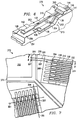
- System 370 may include leads, such as leads 330, 332 and 334, involving a separation in a Z-direction (for orientation 52 in FIGURE 2) and a bonding support mechanism 202.
- leads such as leads 330, 332 and 334, involving a separation in a Z-direction (for orientation 52 in FIGURE 2) and a bonding support mechanism 202.
- bonding wire 328 is shown connecting bonding pad 326 on chip 322 to first lead 330
- bonding wire 329 is shown connecting a pad 327 on chip 322 to a second lead 332.
- Other bonding pads on chip 322 are not shown.
- Chip 322 is shown on a die paddle 372 with a die-attach adhesive 374 between chip 322 and die paddle 372.
- Supporting mechanism 302 may be formed with a support body 315 having features as will be discussed below.
- Bond support mechanism 302 has a trough 303 with a first surface 304 for receiving and supporting the downwardly displaced leads such as lead 330.
- trough 303 has a longitudinal axis 301 substantially perpendicular to a longitudinal axis of the leads, such as axis 305 of lead 309.
- First surface 304 is formed at a first elevation, which refers to a location with respect to the Z-axis for the same axes orientation 52 shown in FIGURE 2.
- Adjacent to first surface 304 is an angled surface 310 that is shaped to accommodate the bend or curvature of stepped portion 338 of the downwardly displaced leads, such as lead 330.
- Support mechanism 302 has a second surface 306 for supporting the straight or planar leads, such as lead 332. The second surface 306 is formed at a second elevation.
- Adjacent to second surface 306 is a third surface 376 for supporting die paddle 372 with chip 322.
- the third surface is formed at a third elevation.
- the leads, such as leads 330, 332, and 334, may be securely held against surfaces 304, 306, and 310, by a clamping mechanism, such as clamping mechanism 200 of FIGURE 6.
- FIGURES 7 and 8 only show a portion of chip 322, the leads associated with chip 322, and support mechanism 302, but it is to be understood that support mechanism 302 would be extended and mirrored to accommodate all the leads associated with chip 322.
- System 370 allows for the chip 322 and paddle 372, along with leads such as leads 330, 332 and 334, to be placed on top of support mechanism 302 which, because of the aligning of surfaces such as step 338 with surface 310, allows for easy positioning of chip 322 and leads 330, 332 and 334 with respect to support mechanism 302 and provides appropriate bonding support. Once bonding is complete with bonding wires 329 and 328, the chip paddle 372, chip 322, and lead fingers 330, 332 and 334 may be removed from the support mechanism 302. Support mechanism 302 provides for quick aligning and full support during the bonding process.
- continuous trough 303 is made possible by the lead tip of the downwardly displaced leads, such as lead tip 336 of lead 304, being pulled back away from the lead tips of the planar leads, such as lead tip 342 of lead 332.
- Manufacturing the leads, e.g. 330, 332, 334, with this feature allows for their placement in mechanism 302 as shown in FIGURES 7 and 8. If a displacement is not as complete, a comb-like approach may be used as shown in FIGURE 9.
- a lead 432 that is substantially planar is shown adjacent to downset lead 430.
- Lead 430 is downset with a stepped portion 438.
- Leads 430 and 432 are shown in use with bonding support system 470 that includes a bonding support mechanism or heating block 402.
- Bonding support mechanism 402 has a first surface 404 for supporting first lead tip 436 of lead 430.
- Bonding support mechanism 402 also includes a second support surface 406 for supporting lead tip 442 of lead 432.
- Surface 406 may be sized and configured to be smaller than lead tip 442.
- a clamping mechanism 499 is shown holding leads 430 and 432 against support mechanism 402 with the clamping positioned just outboard of tape 460. With the support provided by surfaces 404 and 406, bonding wires 428 and 429 may be readily attached.
- FIGURE 9 only shows two leads, it is to be understood that the bonding support mechanism 402 may be duplicated to accommodate all of the leads necessary for a chip, such as chip 322 of FIGURE 7.
Landscapes
- Engineering & Computer Science (AREA)
- Mechanical Engineering (AREA)
- Wire Bonding (AREA)
- Lead Frames For Integrated Circuits (AREA)
- Die Bonding (AREA)
Applications Claiming Priority (2)
| Application Number | Priority Date | Filing Date | Title |
|---|---|---|---|
| US3340796P | 1996-12-18 | 1996-12-18 | |
| US33407P | 1996-12-18 |
Publications (2)
| Publication Number | Publication Date |
|---|---|
| EP0849784A2 true EP0849784A2 (de) | 1998-06-24 |
| EP0849784A3 EP0849784A3 (de) | 1999-02-17 |
Family
ID=21870241
Family Applications (1)
| Application Number | Title | Priority Date | Filing Date |
|---|---|---|---|
| EP97310291A Withdrawn EP0849784A3 (de) | 1996-12-18 | 1997-12-18 | System zum Verbinden eines Leiterrahmens mit einer Halbleitervorrichtung und Trägermechanismus für das Bonden des Leiterrahmens |
Country Status (5)
| Country | Link |
|---|---|
| US (1) | US6068180A (de) |
| EP (1) | EP0849784A3 (de) |
| JP (1) | JPH10189642A (de) |
| KR (1) | KR19980064178A (de) |
| TW (1) | TW404031B (de) |
Cited By (1)
| Publication number | Priority date | Publication date | Assignee | Title |
|---|---|---|---|---|
| US6459130B1 (en) * | 1995-09-29 | 2002-10-01 | Siemens Aktiengesellschaft | Optoelectronic semiconductor component |
Families Citing this family (11)
| Publication number | Priority date | Publication date | Assignee | Title |
|---|---|---|---|---|
| JP3741184B2 (ja) * | 1998-07-27 | 2006-02-01 | 日本テキサス・インスツルメンツ株式会社 | 半導体装置 |
| US6977214B2 (en) * | 1998-12-11 | 2005-12-20 | Micron Technology, Inc. | Die paddle clamping method for wire bond enhancement |
| US6700210B1 (en) * | 1999-12-06 | 2004-03-02 | Micron Technology, Inc. | Electronic assemblies containing bow resistant semiconductor packages |
| US6384487B1 (en) | 1999-12-06 | 2002-05-07 | Micron Technology, Inc. | Bow resistant plastic semiconductor package and method of fabrication |
| US6229202B1 (en) | 2000-01-10 | 2001-05-08 | Micron Technology, Inc. | Semiconductor package having downset leadframe for reducing package bow |
| DE10047897B4 (de) * | 2000-09-26 | 2008-04-24 | Patent-Treuhand-Gesellschaft für elektrische Glühlampen mbH | Elektronische Baueinheit mit einer als Leadframe ausgebildeten Montageplatte und darauf befestigten SMD-Bauteilen |
| JP2004510301A (ja) * | 2000-09-26 | 2004-04-02 | パテント−トロイハント−ゲゼルシヤフト フユア エレクトリツシエ グリユーランペン ミツト ベシユレンクテル ハフツング | 電子ユニットを備えたランプ口金 |
| JP4027135B2 (ja) * | 2002-03-25 | 2007-12-26 | キヤノン株式会社 | インクジェット記録装置 |
| KR100960030B1 (ko) * | 2004-03-12 | 2010-05-28 | 배트 홀딩 아게 | 진공 게이트 밸브 |
| US7777353B2 (en) * | 2006-08-15 | 2010-08-17 | Yamaha Corporation | Semiconductor device and wire bonding method therefor |
| US8796826B2 (en) * | 2011-12-22 | 2014-08-05 | Stmicroelectronics Pte Ltd | Window clamp top plate for integrated circuit packaging |
Family Cites Families (22)
| Publication number | Priority date | Publication date | Assignee | Title |
|---|---|---|---|---|
| US3995845A (en) * | 1972-12-26 | 1976-12-07 | Rca Corporation | Ultrasonic wire bonding chuck |
| US4309849A (en) * | 1978-02-06 | 1982-01-12 | Teledyne Industries, Inc. | Workpiece holder |
| US4378902A (en) * | 1981-02-17 | 1983-04-05 | The Jade Corporation | Apparatus for preventing wire sag in the wire bonding process for producing semiconductor devices |
| US4496965A (en) * | 1981-05-18 | 1985-01-29 | Texas Instruments Incorporated | Stacked interdigitated lead frame assembly |
| JPS6042613B2 (ja) * | 1983-08-08 | 1985-09-24 | 日本電気株式会社 | 半導体装置の製造方法 |
| GB2146935B (en) * | 1983-08-18 | 1986-10-22 | Plessey Co Plc | Jigs for locating electrical components |
| JPS60195945A (ja) * | 1984-03-19 | 1985-10-04 | Hitachi Ltd | ワイヤボンデイング装置 |
| US4891687A (en) * | 1987-01-12 | 1990-01-02 | Intel Corporation | Multi-layer molded plastic IC package |
| US4796078A (en) * | 1987-06-15 | 1989-01-03 | International Business Machines Corporation | Peripheral/area wire bonding technique |
| US4987473A (en) * | 1989-08-03 | 1991-01-22 | Vlsi Technology, Inc. | Leadframe system with multi-tier leads |
| US5054193A (en) * | 1989-08-28 | 1991-10-08 | Hewlett-Packard Company | Printed circuit board fixture and a method of assembling a printed circuit board |
| US5107935A (en) * | 1990-06-08 | 1992-04-28 | Marvin Richard Teaby | Stake setting accessory for jack hammer |
| JPH05144992A (ja) * | 1991-11-18 | 1993-06-11 | Mitsubishi Electric Corp | 半導体装置およびその製造方法ならびにその製造に使用されるリードフレームおよびその製造方法 |
| US5332463A (en) * | 1992-01-15 | 1994-07-26 | Cray Research, Inc. | Self-aligned sealing fixture for use in assembly of microelectronic packages |
| JPH05218283A (ja) * | 1992-02-03 | 1993-08-27 | Nec Corp | 半導体装置 |
| JPH0653277A (ja) * | 1992-06-04 | 1994-02-25 | Lsi Logic Corp | 半導体装置アセンブリおよびその組立方法 |
| JPH06349880A (ja) * | 1993-06-03 | 1994-12-22 | Seiko Epson Corp | ワイヤーボンダー |
| JPH07283265A (ja) * | 1994-04-08 | 1995-10-27 | Toshiba Corp | ボンディング用加熱装置 |
| US5530281A (en) * | 1994-12-21 | 1996-06-25 | Vlsi Technology, Inc. | Wirebond lead system with improved wire separation |
| US5593083A (en) * | 1995-02-14 | 1997-01-14 | International Business Machines Corporation | Castellated nozzle and method of use therof |
| US5558267A (en) * | 1995-03-31 | 1996-09-24 | Texas Instruments Incorporated | Moat for die pad cavity in bond station heater block |
| US5647528A (en) * | 1996-02-06 | 1997-07-15 | Micron Technology, Inc. | Bondhead lead clamp apparatus and method |
-
1997
- 1997-12-16 US US08/991,168 patent/US6068180A/en not_active Expired - Lifetime
- 1997-12-16 KR KR1019970069159A patent/KR19980064178A/ko not_active Withdrawn
- 1997-12-18 JP JP9349710A patent/JPH10189642A/ja active Pending
- 1997-12-18 EP EP97310291A patent/EP0849784A3/de not_active Withdrawn
-
1998
- 1998-03-05 TW TW086119141A patent/TW404031B/zh not_active IP Right Cessation
Cited By (4)
| Publication number | Priority date | Publication date | Assignee | Title |
|---|---|---|---|---|
| US6459130B1 (en) * | 1995-09-29 | 2002-10-01 | Siemens Aktiengesellschaft | Optoelectronic semiconductor component |
| US6927469B2 (en) * | 1995-09-29 | 2005-08-09 | Osram Gmbh | Surface mountable light emitting or receiving device |
| US6975011B2 (en) | 1995-09-29 | 2005-12-13 | Osram Gmbh | Optoelectronic semiconductor component having multiple external connections |
| US7199454B2 (en) | 1995-09-29 | 2007-04-03 | Osram Gmbh | Optoelectronic semiconductor component |
Also Published As
| Publication number | Publication date |
|---|---|
| TW404031B (en) | 2000-09-01 |
| US6068180A (en) | 2000-05-30 |
| EP0849784A3 (de) | 1999-02-17 |
| JPH10189642A (ja) | 1998-07-21 |
| KR19980064178A (ko) | 1998-10-07 |
Similar Documents
| Publication | Publication Date | Title |
|---|---|---|
| US6372625B1 (en) | Semiconductor device having bonding wire spaced from semiconductor chip | |
| US7986047B2 (en) | Wire bond interconnection | |
| US6068180A (en) | System, apparatus, and method for connecting a semiconductor chip to a three-dimensional leadframe | |
| US20010019905A1 (en) | Lead configurations | |
| US20030209815A1 (en) | Semiconductor device and its manufacturing method | |
| JP2954110B2 (ja) | Csp型半導体装置及びその製造方法 | |
| US6625885B1 (en) | Method of making an electrical contact device | |
| US4743956A (en) | Offset bending of curvaceously planar radiating leadframe leads in semiconductor chip packaging | |
| JPS58171839A (ja) | 半導体装置のパツケ−ジ及び実装方法 | |
| US11817374B2 (en) | Electronic device with exposed tie bar | |
| US12489080B2 (en) | Flexible clip with aligner structure | |
| US6006981A (en) | Wirefilm bonding for electronic component interconnection | |
| JPH08148623A (ja) | 半導体装置 | |
| EP0847087A2 (de) | Leiterrahmen | |
| JP2003086621A (ja) | 半導体装置およびその製造方法 | |
| JP3425531B2 (ja) | 電子回路装置及びその製造方法 | |
| JPH11297729A (ja) | 半導体パッケ―ジおよびその形成方法 | |
| JP2006527916A (ja) | リードフレーム、リードフレームを備えた半導体装置及びリードフレームを備えた半導体装置の製造方法 | |
| JP2000216188A (ja) | ワイヤボンディング方法、半導体装置、回路基板、電子機器及びワイヤボンディング装置 | |
| EP0242962A1 (de) | Leiterrahmen für Halbleiter mit asymmetrisch gelegener Insel | |
| JPH05283473A (ja) | フィルムキャリア半導体装置とその製造方法 | |
| JPH09213859A (ja) | 半導体装置の製造方法 | |
| JPH0590320A (ja) | ボール式ワイヤーボンデイング方法 | |
| EP0901164A2 (de) | Verfahren zum Verpacken einer integrierten Schaltung, Verpackungsvorrichtung und Verpackung | |
| JPH0766357A (ja) | リ−ドフレ−ムとその製造方法、及び、このリ−ドフレ−ムを用いた半導体装置 |
Legal Events
| Date | Code | Title | Description |
|---|---|---|---|
| PUAI | Public reference made under article 153(3) epc to a published international application that has entered the european phase |
Free format text: ORIGINAL CODE: 0009012 |
|
| AK | Designated contracting states |
Kind code of ref document: A2 Designated state(s): DE FR GB IT NL |
|
| AX | Request for extension of the european patent |
Free format text: AL;LT;LV;MK;RO;SI |
|
| PUAL | Search report despatched |
Free format text: ORIGINAL CODE: 0009013 |
|
| AK | Designated contracting states |
Kind code of ref document: A3 Designated state(s): AT BE CH DE DK ES FI FR GB GR IE IT LI LU MC NL PT SE |
|
| AX | Request for extension of the european patent |
Free format text: AL;LT;LV;MK;RO;SI |
|
| 17P | Request for examination filed |
Effective date: 19990802 |
|
| AKX | Designation fees paid |
Free format text: DE FR GB IT NL |
|
| 17Q | First examination report despatched |
Effective date: 20020805 |
|
| STAA | Information on the status of an ep patent application or granted ep patent |
Free format text: STATUS: THE APPLICATION IS DEEMED TO BE WITHDRAWN |
|
| 18D | Application deemed to be withdrawn |
Effective date: 20021217 |