EP0849788A2 - Procédé de fabrication d'un article semiconducteur utilisant un substrat ayant une couche d'un semiconducteur poreux - Google Patents
Procédé de fabrication d'un article semiconducteur utilisant un substrat ayant une couche d'un semiconducteur poreux Download PDFInfo
- Publication number
- EP0849788A2 EP0849788A2 EP97310240A EP97310240A EP0849788A2 EP 0849788 A2 EP0849788 A2 EP 0849788A2 EP 97310240 A EP97310240 A EP 97310240A EP 97310240 A EP97310240 A EP 97310240A EP 0849788 A2 EP0849788 A2 EP 0849788A2
- Authority
- EP
- European Patent Office
- Prior art keywords
- layer
- substrate
- semiconductor
- film
- producing
- Prior art date
- Legal status (The legal status is an assumption and is not a legal conclusion. Google has not performed a legal analysis and makes no representation as to the accuracy of the status listed.)
- Granted
Links
Images






Classifications
-
- H—ELECTRICITY
- H10—SEMICONDUCTOR DEVICES; ELECTRIC SOLID-STATE DEVICES NOT OTHERWISE PROVIDED FOR
- H10P—GENERIC PROCESSES OR APPARATUS FOR THE MANUFACTURE OR TREATMENT OF DEVICES COVERED BY CLASS H10
- H10P90/00—Preparation of wafers not covered by a single main group of this subclass, e.g. wafer reinforcement
- H10P90/19—Preparing inhomogeneous wafers
- H10P90/1904—Preparing vertically inhomogeneous wafers
- H10P90/1906—Preparing SOI wafers
- H10P90/1924—Preparing SOI wafers with separation/delamination along a porous layer
-
- B—PERFORMING OPERATIONS; TRANSPORTING
- B28—WORKING CEMENT, CLAY, OR STONE
- B28D—WORKING STONE OR STONE-LIKE MATERIALS
- B28D5/00—Fine working of gems, jewels, crystals, e.g. of semiconductor material; apparatus or devices therefor
-
- H—ELECTRICITY
- H10—SEMICONDUCTOR DEVICES; ELECTRIC SOLID-STATE DEVICES NOT OTHERWISE PROVIDED FOR
- H10F—INORGANIC SEMICONDUCTOR DEVICES SENSITIVE TO INFRARED RADIATION, LIGHT, ELECTROMAGNETIC RADIATION OF SHORTER WAVELENGTH OR CORPUSCULAR RADIATION
- H10F10/00—Individual photovoltaic cells, e.g. solar cells
- H10F10/10—Individual photovoltaic cells, e.g. solar cells having potential barriers
- H10F10/14—Photovoltaic cells having only PN homojunction potential barriers
-
- H—ELECTRICITY
- H10—SEMICONDUCTOR DEVICES; ELECTRIC SOLID-STATE DEVICES NOT OTHERWISE PROVIDED FOR
- H10F—INORGANIC SEMICONDUCTOR DEVICES SENSITIVE TO INFRARED RADIATION, LIGHT, ELECTROMAGNETIC RADIATION OF SHORTER WAVELENGTH OR CORPUSCULAR RADIATION
- H10F71/00—Manufacture or treatment of devices covered by this subclass
- H10F71/121—The active layers comprising only Group IV materials
-
- H—ELECTRICITY
- H10—SEMICONDUCTOR DEVICES; ELECTRIC SOLID-STATE DEVICES NOT OTHERWISE PROVIDED FOR
- H10F—INORGANIC SEMICONDUCTOR DEVICES SENSITIVE TO INFRARED RADIATION, LIGHT, ELECTROMAGNETIC RADIATION OF SHORTER WAVELENGTH OR CORPUSCULAR RADIATION
- H10F71/00—Manufacture or treatment of devices covered by this subclass
- H10F71/139—Manufacture or treatment of devices covered by this subclass using temporary substrates
-
- H—ELECTRICITY
- H10—SEMICONDUCTOR DEVICES; ELECTRIC SOLID-STATE DEVICES NOT OTHERWISE PROVIDED FOR
- H10P—GENERIC PROCESSES OR APPARATUS FOR THE MANUFACTURE OR TREATMENT OF DEVICES COVERED BY CLASS H10
- H10P10/00—Bonding of wafers, substrates or parts of devices
- H10P10/12—Bonding of semiconductor wafers or semiconductor substrates to semiconductor wafers or semiconductor substrates
- H10P10/128—Bonding of semiconductor wafers or semiconductor substrates to semiconductor wafers or semiconductor substrates by direct semiconductor to semiconductor bonding
-
- H—ELECTRICITY
- H10—SEMICONDUCTOR DEVICES; ELECTRIC SOLID-STATE DEVICES NOT OTHERWISE PROVIDED FOR
- H10P—GENERIC PROCESSES OR APPARATUS FOR THE MANUFACTURE OR TREATMENT OF DEVICES COVERED BY CLASS H10
- H10P52/00—Grinding, lapping or polishing of wafers, substrates or parts of devices
-
- H—ELECTRICITY
- H10—SEMICONDUCTOR DEVICES; ELECTRIC SOLID-STATE DEVICES NOT OTHERWISE PROVIDED FOR
- H10P—GENERIC PROCESSES OR APPARATUS FOR THE MANUFACTURE OR TREATMENT OF DEVICES COVERED BY CLASS H10
- H10P74/00—Testing or measuring during manufacture or treatment of wafers, substrates or devices
-
- H—ELECTRICITY
- H10—SEMICONDUCTOR DEVICES; ELECTRIC SOLID-STATE DEVICES NOT OTHERWISE PROVIDED FOR
- H10P—GENERIC PROCESSES OR APPARATUS FOR THE MANUFACTURE OR TREATMENT OF DEVICES COVERED BY CLASS H10
- H10P90/00—Preparation of wafers not covered by a single main group of this subclass, e.g. wafer reinforcement
- H10P90/19—Preparing inhomogeneous wafers
- H10P90/1904—Preparing vertically inhomogeneous wafers
- H10P90/1906—Preparing SOI wafers
- H10P90/1914—Preparing SOI wafers using bonding
-
- H—ELECTRICITY
- H10—SEMICONDUCTOR DEVICES; ELECTRIC SOLID-STATE DEVICES NOT OTHERWISE PROVIDED FOR
- H10P—GENERIC PROCESSES OR APPARATUS FOR THE MANUFACTURE OR TREATMENT OF DEVICES COVERED BY CLASS H10
- H10P90/00—Preparation of wafers not covered by a single main group of this subclass, e.g. wafer reinforcement
- H10P90/19—Preparing inhomogeneous wafers
- H10P90/1904—Preparing vertically inhomogeneous wafers
- H10P90/1906—Preparing SOI wafers
- H10P90/1914—Preparing SOI wafers using bonding
- H10P90/1916—Preparing SOI wafers using bonding with separation or delamination along an ion implanted layer, e.g. Smart-cut
-
- H—ELECTRICITY
- H10—SEMICONDUCTOR DEVICES; ELECTRIC SOLID-STATE DEVICES NOT OTHERWISE PROVIDED FOR
- H10W—GENERIC PACKAGES, INTERCONNECTIONS, CONNECTORS OR OTHER CONSTRUCTIONAL DETAILS OF DEVICES COVERED BY CLASS H10
- H10W10/00—Isolation regions in semiconductor bodies between components of integrated devices
- H10W10/10—Isolation regions comprising dielectric materials
- H10W10/181—Semiconductor-on-insulator [SOI] isolation regions, e.g. buried oxide regions of SOI wafers
-
- G—PHYSICS
- G02—OPTICS
- G02F—OPTICAL DEVICES OR ARRANGEMENTS FOR THE CONTROL OF LIGHT BY MODIFICATION OF THE OPTICAL PROPERTIES OF THE MEDIA OF THE ELEMENTS INVOLVED THEREIN; NON-LINEAR OPTICS; FREQUENCY-CHANGING OF LIGHT; OPTICAL LOGIC ELEMENTS; OPTICAL ANALOGUE/DIGITAL CONVERTERS
- G02F1/00—Devices or arrangements for the control of the intensity, colour, phase, polarisation or direction of light arriving from an independent light source, e.g. switching, gating or modulating; Non-linear optics
- G02F1/01—Devices or arrangements for the control of the intensity, colour, phase, polarisation or direction of light arriving from an independent light source, e.g. switching, gating or modulating; Non-linear optics for the control of the intensity, phase, polarisation or colour
- G02F1/13—Devices or arrangements for the control of the intensity, colour, phase, polarisation or direction of light arriving from an independent light source, e.g. switching, gating or modulating; Non-linear optics for the control of the intensity, phase, polarisation or colour based on liquid crystals, e.g. single liquid crystal display cells
- G02F1/133—Constructional arrangements; Operation of liquid crystal cells; Circuit arrangements
- G02F1/136—Liquid crystal cells structurally associated with a semi-conducting layer or substrate, e.g. cells forming part of an integrated circuit
- G02F1/1362—Active matrix addressed cells
- G02F1/136277—Active matrix addressed cells formed on a semiconductor substrate, e.g. of silicon
-
- H—ELECTRICITY
- H10—SEMICONDUCTOR DEVICES; ELECTRIC SOLID-STATE DEVICES NOT OTHERWISE PROVIDED FOR
- H10P—GENERIC PROCESSES OR APPARATUS FOR THE MANUFACTURE OR TREATMENT OF DEVICES COVERED BY CLASS H10
- H10P72/00—Handling or holding of wafers, substrates or devices during manufacture or treatment thereof
- H10P72/70—Handling or holding of wafers, substrates or devices during manufacture or treatment thereof for supporting or gripping
- H10P72/74—Handling or holding of wafers, substrates or devices during manufacture or treatment thereof for supporting or gripping using temporarily an auxiliary support
- H10P72/7432—Handling or holding of wafers, substrates or devices during manufacture or treatment thereof for supporting or gripping using temporarily an auxiliary support used in a transfer process involving transfer directly from an origin substrate to a target substrate without use of an intermediate handle substrate
-
- H—ELECTRICITY
- H10—SEMICONDUCTOR DEVICES; ELECTRIC SOLID-STATE DEVICES NOT OTHERWISE PROVIDED FOR
- H10P—GENERIC PROCESSES OR APPARATUS FOR THE MANUFACTURE OR TREATMENT OF DEVICES COVERED BY CLASS H10
- H10P72/00—Handling or holding of wafers, substrates or devices during manufacture or treatment thereof
- H10P72/70—Handling or holding of wafers, substrates or devices during manufacture or treatment thereof for supporting or gripping
- H10P72/74—Handling or holding of wafers, substrates or devices during manufacture or treatment thereof for supporting or gripping using temporarily an auxiliary support
- H10P72/7434—Handling or holding of wafers, substrates or devices during manufacture or treatment thereof for supporting or gripping using temporarily an auxiliary support used in a transfer process involving at least two transfer steps, i.e. including an intermediate handle substrate
-
- Y—GENERAL TAGGING OF NEW TECHNOLOGICAL DEVELOPMENTS; GENERAL TAGGING OF CROSS-SECTIONAL TECHNOLOGIES SPANNING OVER SEVERAL SECTIONS OF THE IPC; TECHNICAL SUBJECTS COVERED BY FORMER USPC CROSS-REFERENCE ART COLLECTIONS [XRACs] AND DIGESTS
- Y02—TECHNOLOGIES OR APPLICATIONS FOR MITIGATION OR ADAPTATION AGAINST CLIMATE CHANGE
- Y02E—REDUCTION OF GREENHOUSE GAS [GHG] EMISSIONS, RELATED TO ENERGY GENERATION, TRANSMISSION OR DISTRIBUTION
- Y02E10/00—Energy generation through renewable energy sources
- Y02E10/50—Photovoltaic [PV] energy
- Y02E10/547—Monocrystalline silicon PV cells
-
- Y—GENERAL TAGGING OF NEW TECHNOLOGICAL DEVELOPMENTS; GENERAL TAGGING OF CROSS-SECTIONAL TECHNOLOGIES SPANNING OVER SEVERAL SECTIONS OF THE IPC; TECHNICAL SUBJECTS COVERED BY FORMER USPC CROSS-REFERENCE ART COLLECTIONS [XRACs] AND DIGESTS
- Y02—TECHNOLOGIES OR APPLICATIONS FOR MITIGATION OR ADAPTATION AGAINST CLIMATE CHANGE
- Y02P—CLIMATE CHANGE MITIGATION TECHNOLOGIES IN THE PRODUCTION OR PROCESSING OF GOODS
- Y02P70/00—Climate change mitigation technologies in the production process for final industrial or consumer products
- Y02P70/50—Manufacturing or production processes characterised by the final manufactured product
Definitions
- This invention relates to a process for producing a semiconductor article that can suitably be used for producing a semiconductor device such as a semiconductor integrated circuit, a solar cell, a semiconductor laser device or a light emitting diode. More particularly, it relates to a process for producing a semiconductor article having a step of separating a substrate.
- Semiconductor articles are popular in terms of semiconductor wafers, semiconductor substrates and various semiconductor devices and include those adapted for producing semiconductor devices by utilizing the semiconductor region thereof and those used as preforms for producing semiconductor devices.
- Some semiconductor articles of the type under consideration comprise a semiconductor layer arranged on an insulator.
- SOI silicon on insulator
- Vth threshold voltage
- a device formed on a compound semiconductor shows a remarkable level of performance that cannot be expected from silicon particularly in terms of high speed operation and light emission.
- Such devices are currently formed by means of epitaxial growth on a compound semiconductor substrate that may be made of GaAs or a similar compound.
- a compound semiconductor substrate is costly and mechanically not very strong so that it is not adapted to produce a large wafer.
- the FIPOS method comprises steps of forming an islanded N-type Si layer on a P-type single crystal Si substrate by proton/ion implantation (Imai et al., J. Crystal Growth, Vol.
- the oxygen ion implantation method is also referred to the SIMOX method, which was proposed by K. Izumi for the first time.
- SIMOX method oxygen ions are implanted into an Si wafer to a concentration level of 10 17 to 10 18 /cm 2 and then the latter is annealed at high temperature of about 1,320°C in an argon/oxygen atmosphere.
- the implanted oxygen ions are chemically combined with Si atoms to produce a silicon oxide layer that is centered at a depth corresponding to the projection range (Rp) of the implanted ions.
- Rp projection range
- the surface Si layer used to show a defect rate as high as 10 5 /cm 2 While the surface Si layer used to show a defect rate as high as 10 5 /cm 2 , a recent technological development has made it possible to reduce the defect rate down to about 10 2 /cm 2 by selecting a rate of oxygen implantation of about 4 ⁇ 10 17 /cm 2 .
- the allowable range of energy infusion and that of ion implantation are limited if the film quality of the Si oxide layer and the crystallinity of the surface Si layer are to be held to respective desired levels and hence the film thickness of the surface Si layer and that of the buried Si oxide (BOX; buried oxide) layer are allowed to take only limited values.
- a process of sacrifice oxidation or epitaxial growth is indispensable to realize a surface Si layer having a desired film thickness. Such a process by turn gives rise to a problem of uneven film thickness due to the intrinsic adverse effect of the process.
- SIMOX can produce defective Si oxide regions in the Si oxide layer that are referred to as pipes.
- One of the possible causes of the phenomenon may be foreign objects such as dust introduced into the layer at the time of ion implantation.
- the device produced in a pipe region can show degraded characteristics due to the leak current between the active layer and the underlying substrate.
- the SIMOX technique involves the use of a large volume of ions that is by far greater than the volume used in the ordinary semiconductor process and hence the ion implantation process may take a long time if a specifically designed apparatus is used for it. Since the ion implantation process is performed typically by means of raster scan of an ion beam showing a predetermined flow rate of electric current or by spreading an ion beam, a long time may be required for processing a large wafer. Additionally, when a large wafer is processed at high temperature, the slip problem due to an uneven temperature distribution within the wafer can become very serious.
- the mean deviation in the film thickness can be as large as tens of several percent to make the technique unfeasible when the film is thinned to an order of sub-micrometer. This problem will become more remarkable for wafers having a large diameter.
- the technique of (2) is typically used in combination with that of (1). More specifically, the film is thinned by means of the technique of (1) to about 1 to 3 ⁇ m and the distribution of film thickness is determined by observing the film thickness at a number of points. Then, the film is subjected to an etching operation where the film is scanned with plasma of SF 6 particles having a diameter of several millimeters, correcting the distribution of film thickness, until a desired film thickness is obtained.
- the distribution of film thickness can be confined within about ⁇ 10nm or less by means of this technique.
- this process is accompanied by a drawback that, if foreign objects are present on the substrate in the form of particles during the plasma etching, they operate as so many etching masks to produce projections on the substrate when the etching operation is over.
- the substrate shows a coarse surface immediately after the etching operation
- a touch-polishing operation has to be conducted on the surface after the end of the plasma etching and the operation is controlled only in terms of its duration. Then, again the problem of deviations in the film thickness due to polishing arises.
- a polishing agent typically containing colloidal silica is used for the polishing operation and hence the layer for making an active layer is directly scraped by the polishing agent so that a crushed and/or distorted layer may be produced.
- the throughput of the process can be significantly reduced when large wafers are treated because the duration of the plasma etching operation is prolonged as a function of the surface area of the wafer being processed.
- the technique of (3) involves the use of a film configuration for the substrate to be thinned that comprises one or more than one film layers adapted to selective etching.
- a P + -Si thin layer containing boron by more than 10 19 /cm 3 and a P-type Si thin layer are made to grow sequentially on a P-type substrate by means of epitaxial growth to produce a first substrate, which is then bonded to a second substrate with an insulation layer interposed therebetween, the insulation layer being typically an oxide film, and that the rear surface of the first substrate is made sufficiently thin in advance by scraping and polishing.
- the P + -layer is made to become exposed by selectively etching the overlying P-type layer and then the P-type substrate is made to become exposed by selectively etching the P + -layer to produce an SOI structure.
- Maszara W. P. Maszara, J. Electrochem. Soc., Vol. 138,341 (1991)).
- the inventors of the present invention proposed a novel method of manufacturing a semiconductor article in Japanese Patent Application Laid-Open No. 5-21338.
- the proposed method is characterized by comprising steps of forming an article by arranging a nonporous single crystal semiconductor region on a porous single crystal semiconductor region, bonding the surface of a material carrying an insulating material thereon to the corresponding surface of said porous single crystal semiconductor region and subsequently removing said porous single crystal semiconductor region by etching.
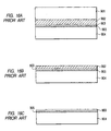
- the proposed method uses a porous layer 902 formed on a first Si substrate 901 as a layer to be selectively etched. After forming a nonporous single crystal Si layer 903 on the porous layer 902 by epitaxial growth, it is bonded to a second substrate 904 with an Si oxide layer 905 interposed therebetween (Fig. 16A). Then, the porous Si layer is made to become exposed over the entire surface area of the first substrate by scraping off the first substrate from the rear side (Fig. 16B). The exposed porous Si is then etched out by means of a selective etching solution typically containing KOH or HF+H 2 O 2 (Fig. 16C).
- the nonporous single crystal Si layer formed on the porous layer in advance can be transferred onto the second substrate to produce an SOI substrate without reducing the thickness of the nonporous single crystal Si layer.
- the uniformity of the film thickness of the SOI substrate is determined during the epitaxial growth step. According to a report by Sato et al., since a CVD system adapted to an ordinary semiconductor process can be used for the epitaxial growth, a degree of uniformity of the film thickness as high as 100nm ⁇ 2% can be realized. Additionally, the epitaxial Si layer shows an excellent crystallinity of about 3.5 ⁇ 10 2 /cm 2 .
- the selectivity of any conventional selective etching technique heavily depends on the concentration difference among the impurities contained in the substrate and the steepness of the concentration profile of the impurities along the depth of the substrate as described above, the temperature of the heat treatment (for bonding, epitaxial growth, oxidation and so on) is limited to as low as 800°C at most because the impurity concentration profile becomes flattened above that temperature limit.
- the etching rate of the proposed etching technique is mainly determined by the structural difference between the porous layer and the bulk layer so that the heat treatment is not subjected to such a rigorous limitation and temperature as high as 1,180°C can be used.
- a semiconductor substrate to be produced by way of a bonding process inevitably requires at least two wafers as starting materials, one of which is substantially wasted away in the course of polishing and etching to consume the limited natural resources almost for nothing.
- an SOI manufacturing process is required to realize low cost and economic feasibility in addition to an enhanced degree of process controllability and an improved uniformity of the film thickness.
- the requirements of a process for manufacturing a high quality SOI substrate include an excellent reproducibility, an enhanced level of resource saving capability through the repeated use of a same wafer and low manufacturing cost.
- a surface layer of a first Si substrate 1001 is made porous to form porous layer 1002, and thereon single crystal Si layer 1003 is formed.
- This single crystal Si layer on the first Si substrate is bonded to the main face of second Si substrate 1004 with interposition of insulation layer 1005 (Fig. 17A). Then the wafer is separated at the porous layer (Fig. 17B). The bared porous Si layer on the second substrate surface is removed selectively to form an SOI substrate (Fig. 17C).
- First substrate 1001 can be used again after removal of the porous layer.
- the substrates is separated by utilizing the brittleness of the porous silicon layer in comparison with the nonporous silicon layer, enabling reuse of the substrate once used for semiconductor substrate production process to lower the production cost.
- Japanese Patent Application Laid-Open No. 8-213645 discloses a process in which a semiconductor layer is formed, on a porous silicon layer, for photoelectric conversion portion of a solar cell and the semiconductor layer is later separated at the porous layer to reuse the substrate having the porous silicon layer.
- the semiconductor layer is bonded to a rigid jig with an adhesive, and the silicon substrate having the formed porous silicon layer is bonded to another rigid jig, and thereafter the jigs are pulled respectively in opposite directions to separate the semiconductor layer from the porous layer.
- the force is required for pulling the jigs to separate the entire face of the wafer in a stroke. Since the required pulling force is proportional to square of the wafer diameter, a larger wafer diameter requires a larger pulling force for the separation. Further, owing to the lower flexibility and to the difficulty in control of the force, the separation cannot easily be caused at the desired region.
- the substrate for the element is desirably inexpensive in view of the production cost.
- silicon is used as the semiconductor constituting the solar cell.
- single crystal silicon is most suitable from the standpoint of photoelectric conversion efficiency.
- amorphous silicon is advantageous for the larger cell area and the lower cell production cost.
- polycrystal silicon is being investigated for achieving a low production cost like the amorphous silicon, and a high energy-conversion efficiency like the single crystal silicon.
- the crystal mass is sliced into substrate plates, so that the thickness of the substrate is limited to not less than 0.3 mm. This thickness is much larger than that necessary for absorbing the luminous energy sufficiently. Therefore, the material is not effectively utilized. For the lower production cost, further decrease of the thickness is desired.
- a method of silicon sheet formation by spinning has been disclosed in which liquid droplets of molten silicon are introduced into a mold to form a sheet. In this method, the thickness of the obtained sheet is about 0.1 to 0.2 mm, which is still thicker than the necessary and sufficient thickness (20 ⁇ m to 50 ⁇ m).
- a thin epitaxial layer, grown on a single crystal silicon substrate and separated (peeled) from the substrate, is used for the solar cell to achieve a higher energy conversion efficiency and a lower production cost (Milnes, A.G. and Feucht D.L.: "Peeled Film Technology Solar Cells", IEEE Photovoltaic Specialist Conference, p.338, 1975).
- an intermediate layer of SiGe is formed between the single crystal silicon as the substrate and the grown epitaxial layer, and after the heteroepitaxial growth, the grown layer is peeled by selective melting of the interlayer.
- heteroepitaxial growth is generally not advantageous in production cost because of liability of causing defects in the growth interface owing to the difference of the lattice constants, and because of the use of different materials.
- USP 4,816,420 discloses a process for producing a thin crystal solar cell.
- a sheet-shaped crystal is formed through a mask, on a crystal substrate, by selective epitaxial growth and lateral growth, and the resulting sheet is separated from the substrate.
- the apertures of the mask is provided in lines, the crystal is grown by line seeding by selective epitaxial growth and lateral growth, and the crystal sheet is peeled mechanically by utilizing cleavage of the crystal. Therefore, at a size of the line seed larger than a certain limit, the larger contact area of the crystal sheet with the substrate tends to cause breakage of the crystal sheet during the peeling operation.
- this method cannot be applied practically even at the smallest aperture line width (practically about 1 ⁇ m) at the line length of several millimeters to several centimeters or more.
- Japanese Patent Application Laid-Open No. 6-45622 applied by the inventors of the present invention discloses a solar cell production process in which a porous silicon layer is formed by anodization on a surface of a silicon wafer, the porous silicon layer is peeled and is fixed onto a metal substrate, an epitaxial layer is formed on the porous layer to obtain a thin film crystal solar cell having excellent properties.
- this method is not satisfactory since the metal substrate is treated at a high temperature, and thereby the epitaxial layer can be contaminated with impurities.
- Japanese Patent Application Laid-Open No. 5-211128 discloses another process for separation of a substrate by use of a bubble layer which is different from the aforementioned porous layer but has a function similar thereto.
- a bubble layer is formed in a silicon substrate by ion implantation, crystal rearrangement and bubble coalescence are caused in the bubble layer by heat treatment, and the surface region of the silicon substrate (called a thin semiconductor film) is stripped off at the bubble layer.
- the thin semiconductor film in this disclosure means an outermost region of a bulk Si where no or few implanted ions are present.
- This process should be conducted at a temperature where the crystal rearrangement and the bubble coalescence occur effectively. It is not easy to establish the ion implantation conditions and to optimize the heat treatment of this process.
- the object of the present invention is to provide a process for producing a semiconductor article comprising a separation of a substrate where a part of the separated substrate is reused as the material for the semiconductor article.
- a process for producing a semiconductor article comprising bonding a film onto a substrate having a porous semiconductor layer, and separating the film from the substrate at the porous semiconductor layer by applying a force to the film in a peeling direction.
- a process for producing a semiconductor article comprising bonding a film onto a first substrate having a porous semiconductor layer and a nonporous semiconductor layer, and separating the nonporous semiconductor layer from the first substrate at the porous semiconductor layer by applying a force to the film in a peeling direction.
- a process for producing a semiconductor article comprising bonding a film onto a first substrate having a porous semiconductor layer and a nonporous semiconductor layer, separating the nonporous semiconductor layer from the first substrate at the porous semiconductor layer by applying a force to the film in a peeling direction, and bonding the separated nonporous semiconductor layer onto a second substrate.
- the substrate recovered by the separation of the nonporous semiconductor layer and removal of the remaining porous layer from the first substrate can be used again as the material for the first substrate in the present invention.
- the reuse of the substrate can also be possible in the embodiment in which the porous layer is separated from the substrate.
- the substrate is separated by utilizing the fragility of the porous semiconductor layer.
- the film is separated at the porous layer from the substrate by applying a force to the film in a direction of peeling the film from the substrate.
- the separation of the substrate can readily be conducted by peeling gradually the film from the edge of the substrate to concentrate the peeling force at the front of the peeling portion, whereas simple mechanical separation in a conventional method may cause breakage of the wafer. In the method of the present invention, the wafers are rarely broken.
- the separation is conducted by utilizing simply the fragility of the porous layer in the present invention, complicated physical phenomena such as coalescence of bubbles in the heat treatment need not be considered for process optimization. Therefore, the substrate can be separated effectively in a simple manner.
- a layer or layers on the substrate can be transferred from the substrate onto a film. This method can be applied to various uses.
- the process for producing a semiconductor article of the present invention reuses the substrate repeatedly for effective material utilization, providing semiconductor articles such as SOI substrates, and solar cells at a low cost.
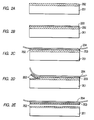
- Figs. 1A, 1B, 1C, and 1D are schematic sectional views for explaining the embodiment of the present invention.
- Figs. 2A, 2B, 2C, 2D, and 2E are schematic sectional views for explaining another embodiment of the present invention.
- Figs. 3A, 3B, 3C, and 3D are schematic sectional views for explaining still another embodiment of the present invention.
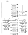
- Fig. 4 shows schematic sectional views for explaining the process of still another embodiment of the present invention.
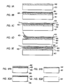
- Figs. 5A, 5B, 5C, 5D, 5E, 5FA, 5FB, 5GA, and 5GB are schematic sectional views for explaining still another embodiment of the present invention.
- Figs. 6A, 6B, 6C, 6D, 6EA, 6EB, 6FA, and 6FB are schematic sectional views for explaining still another embodiment of the present invention.
- Figs. 7A, 7B, 7C, 7D, 7E, 7FA, 7FB, 7GA, and 7GB are schematic sectional views for explaining still another embodiment of the present invention.
- Figs. 8A, 8B, 8C, 8D, 8E, 8FA, 8FB, 8GA, and 8GB are schematic sectional views for explaining still another embodiment of the present invention.
- Figs. 9A, 9B, 9CA, 9CB, 9CC, 9DA, 9DB, and 9DC are schematic sectional views for explaining still another embodiment of the present invention.
- Fig. 10 is a schematic sectional view showing a structure of a solar cell prepared by employing the process of semiconductor article of the present invention.
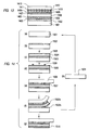
- Fig. 11 is a drawing for explaining a process for producing a solar cell according to the process of the present invention.
- Fig. 12 is a drawing for explaining another process for producing a solar cell according to the process of the present invention.
- Fig. 13 is a schematic sectional view showing the structure of the GaAs/AlGaAs thin film solar cell formed on the porous layer produced by the process explained by Fig. 12.
- Fig. 14 is a drawing for explaining a process for producing a solar cell according to the process of the present invention.
- Fig. 15 is a drawing for explaining another process for producing a solar cell according to the process of the present invention.
- Figs. 16A, 16B, and 16C are drawings for explaining a prior art process.
- Figs. 17A, 17B, and 17C are drawings for explaining another prior art process.
- Silicon (Si) is suitably used as the material for the porous semiconductor layer.
- Porous Si was firstly discovered in 1956 by Uhlir et al. who were studying a process of electropolishing a semiconductor material (A. Uhlir, Bell Syst. Tech. J., Vol. 35,333 (1956)). Porous Si can be prepared through anodization of an Si substrate in an HF solution. Unagami reports as a result of his study on the dissolutive reaction of Si in an Si anodization process that the existence of holes is required for anodization of Si and the reaction proceeds in a manner as described below (T. Unagami, J. Electrochem. Soc., Vol. 127,476 (1980)).
- N-type Si can be made porous under the existence of holes whereas N-type Si cannot be made porous, in reality, both N-type Si and P-type Si can be turned porous under certain conditions.
- single crystal porous Si can be formed through anodization of a single crystal Si substrate typically in an HF solution.
- a porous Si layer shows a spongy structure where pores with a diameter between 10 -1 and 10nm are arranged with intervals between 10 -1 and 10nm.
- the density of porous Si can be made to vary between 2.1 and 0.6g/cm 3 by varying the concentration of the HF solution between 50 and 20% and/or by varying the current density in contrast to the density of single crystal Si that is equal to 2.33g/cm 3 .
- the porosity of porous Si is variable. While porous Si can be made to show a density less than a half of that of single crystal Si, it maintains the properties as single crystal Si so that a single crystal Si layer can be formed by epitaxial growth on a porous Si layer.
- a porous Si layer has a density that is less than the density of a single crystal Si layer because it contains a large number of voids in the inside. Consequently, a porous Si layer shows a dramatically large surface area relative to the volume it occupies. This means that a porous Si layer can be etched at a rate by far greater than the rate at which an ordinary single crystal Si layer is normally etched.
- porous Si shows a mechanical strength that varies depending on its porosity, it is presumably lower than that of bulk Si. For instance, if a porous Si layer shows a porosity of 50%, it may be safe to assume that its mechanical strength is about a half of that of a comparable bulk Si layer. In other words, when a wafer formed by bonding a pair of substrates is subjected to compressive, tensile or shearing force, the porous Si layer arranged therebetween will be destroyed firstly. If the layer has a large porosity, it will be destroyed with little effort.
- the porous layer can be formed in layers of different porosities by varying the current density during the anodization. Otherwise, porous layer can be formed in a thickness larger than a high impurity concentration layer by forming a high impurity concentration layer on one face of the Si substrate and anodizing this face.
- micro-cavities having a diameter between several nanometers and tens of several namometers can be formed in a piece of bulk Si to a concentration of 10 16-17 /cm 3 by implanting helium or hydrogen ions and heat treating the piece particularly in the area where ions are implanted (see, inter alia, A. Van Veen, C. C. Griffioen and J. H. Evans, Mat. Res. Soc. Symp. Proc. 107 (1988, Material Res. Soc. Pittsburgh, Pennsylvania) p. 449).
- Recently, a number of researches are being conducted for utilizing a group of micro-cavities for a gettering site of a metal impurity.
- the thickness of the surface Si layer and that of the buried Si oxide layer are limited to respective ranges that allow both the formation of a micro-cavity group and relaxation of the stress generated by the increased volume at the time of oxidation and an operation of forming a groove is necessary for selective oxidation so that an SOI structure cannot be produced on the entire surface of the substrate.
- the porous semiconductor layer of the present invention includes such a layer having micro-cavities or micro-bubbles.
- the film employed in the present invention includes adhesive resin films such as polyimide films, electroconductive resin films, electroconductive metal films, films which change adhesiveness by action of optical energy, electronic rays, heat, or the like, and aluminum foil-containing glass cloth film, but is not limited thereto.
- adhesive resin films such as polyimide films, electroconductive resin films, electroconductive metal films, films which change adhesiveness by action of optical energy, electronic rays, heat, or the like, and aluminum foil-containing glass cloth film, but is not limited thereto.
- Specific examples are Tefzel films produced by DuPont Co., aluminum foil glass cloth tapes (No. 363) and heat-resistant aluminum foil tapes (No. 433) produced by Scotch Co., and release tapes (No. 3200A, No. 31RH, and BT-315) produced by Nitto Denko Co.
- an adhesive may be employed to supplement the adhesion force, if the adhesive force is not sufficient.
- the adhesive includes resin type adhesives like epoxy type adhesives, waxes, SOG (s
- the thickness of the film in the present invention is selected suitably depending on the material and properties of the film employed, and is in the range preferably from 5 ⁇ m to 3 cm, more preferably from 10 ⁇ m to 1 cm.
- a nonporous semiconductor layer can be formed preferably by using a material selected from single crystal Si, polycrystalline Si, noncrystalline Si and compound semiconductors including GaAs, InP, GaAsP, GaAlAs, InAs, AlGaSb, InGaAs, ZnS, CdSe, CdTe and SiGe.
- a nonporous semiconductor layer that can be used for the purpose of the present invention may substantially contain one or more than one FETs (field effect transistors).
- the first substrate may be prepared by forming a nonporous semiconductor layer on the porous silicon layer in the silicon substrate or by forming a porous silicon layer in part of a silicon substrate having therein a nonporous semiconductor substrate.
- the first substrate includes not only substrates comprised of a silicon substrate having an ion implantation layer generating Micro-bubbles formed therein and a nonporous semiconductor layer, but also substrates having additionally an insulation layer such as a nitride film and an oxide film, substrates having an epitaxial semiconductor layer and an insulation layer formed on a silicon substrate and an ion implantation layer formed by subsequent ion implantation into the silicon substrate, substrates having a nonporous semiconductor layer formed on the silicon substrate and an ion implantation layer formed by subsequent ion implantation, and the like substrates.
- substrates comprised of a silicon substrate having an ion implantation layer generating Micro-bubbles formed therein and a nonporous semiconductor layer, but also substrates having additionally an insulation layer such as a nitride film and an oxide film, substrates having an epitaxial semiconductor layer and an insulation layer formed on a silicon substrate and an ion implantation layer formed by subsequent ion implantation into the silicon substrate, substrates having a
- the epitaxial growth method for the silicon layer formation on the porous layer in the present invention includes thermal CVD, LPCVD, sputtering, plasma CVD, photo-assisted CVD, and liquid phase growth.
- the source gas typically includes silanes and halogenated silanes such as SiH 2 Cl 2 , SiCl 4 , SiHCl 3 , SiH 4 , Si 2 H 6 , SiH 2 F 2 , and Si 2 F 6 .
- silanes and halogenated silanes such as SiH 2 Cl 2 , SiCl 4 , SiHCl 3 , SiH 4 , Si 2 H 6 , SiH 2 F 2 , and Si 2 F 6 .
- hydrogen (H 2 ) is added as the carrier gas or for reducing atmosphere formation.
- the ratio of the source gas to the hydrogen gas is selected suitably depending on the layer formation method, the kind of the source gas, and the layer formation conditions, and is in the range preferably from 1:10 to 1:1000 (introduction flow rate ratio), more preferably from 1:20 to 1:800.
- silicon is dissolved in a solvent like Ga, In, Sb, Bi, and Sn under an H 2 or N 2 atmosphere, and the epitaxial growth is allowed to proceed by cooling gradually the solvent or causing temperature difference in the solvent.
- MOCVD Metal Organic Chemical Vapor deposition
- MBE liquid phase growth
- the source material for the crystal growth is selected suitably depending on the kind of the compound semiconductor and the growth method.
- GaAs formation Ga(CH 3 ) 3 , AsH 3 , Al(CH 3 ) 3 , or the like is used in MOCVD.
- liquid phase growth the growth is conducted by dissolving As, or As and Al in Ga as the solvent.
- the temperature and the pressure are selected depending on the formation process and the source gas.
- the temperature is preferably in the range of from about 800°C to 1250°C, more preferably from 850°C to 1200°C.
- the temperature depends on the solvent.
- the temperature is preferably in the range of from 600°C to 1050°C.
- the temperature is preferably in the range from 650°C to 850°C.
- the temperature is preferably in the range of from 650°C to 900°C.
- the temperature is in the range preferably from 200°C to 600°C, more preferably from 200°C to 500°C.
- the pressure is in the range preferably from 10 -2 Torr to 760 Torr, more preferably from 10 -1 Torr to 760 Torr with exception of MBE.
- the evacuation pressure is preferably not higher than 10 -5 Torr, more preferably not higher than 10 -6 Torr.
- the second substrate onto which the nonporous semiconductor layer is to be transferred includes semiconductor substrates such as single crystal silicon substrates, substrates having an insulation film such as an oxide film (including thermal oxidation film) and a nitride film, light-transmissive substrates such as a silica glass substrate and a glass substrate, metal substrates, insulating substrate such as alumina, and like substrates.
- semiconductor substrates such as single crystal silicon substrates, substrates having an insulation film such as an oxide film (including thermal oxidation film) and a nitride film, light-transmissive substrates such as a silica glass substrate and a glass substrate, metal substrates, insulating substrate such as alumina, and like substrates.
- the second substrate is selected suitably depending on the application field of the semiconductor article.
- the aforementioned non-porous semiconductor layer on the film is bonded to a second substrate to obtain a multiple layer structure with the nonporous semiconductor layer placed inside.
- the multiple layer structure having a nonporous semiconductor layer placed inside includes not only the structures in which the nonporous semiconductor layer on the film separated from the first substrate is bonded directly to the second substrate but also the structures in which an oxide film, a nitride film, or the like formed on the surface of the nonporous semiconductor layer surface is bonded to the second substrate. That is, the structure having a nonporous semiconductor layer placed inside means a multiple layer structure in which the nonporous semiconductor layer is placed inside the film or the supporting member in the multiple layer structure.
- the non-porous semiconductor layer and the second substrate can be bonded together, for example, at room temperature by making the both bonding faces flat and bringing the both into close contact with each other.
- Anode bonding, pressing, or heat treatment may be employed for stronger bonding.
- the residual porous Si remaining on the substrates can be selectively removed on the basis of the fact that the porous Si layer has a low mechanical strength and a large surface area.
- Methods that can be used for selectively removing the remaining porous Si include mechanical techniques such as scraping and polishing, chemical etching using an etching solution and ion etching (such as reactive ion etching).
- Etching solutions that can be used for a process of selectively removing the porous Si by means of an etching solution include, beside a mixture solution of 49% hydrofluoric acid and 30% aqueous hydrogen peroxide, hydrofluoric acid, a mixture solution obtained by adding alcohol to hydrofluoric acid, a mixture solution obtained by adding alcohol and aqueous hydrogen peroxide to hydrofluoric acid, buffered hydrofluoric acid, a mixture solution obtained by adding alcohol to buffered hydrofluoric acid, a mixture solution obtained by adding aqueous hydrogen peroxide to buffered hydrofluoric acid, a mixture solution obtained by adding alcohol and aqueous hydrogen peroxide to buffered hydrofluoric acid and a mixture solution of hydrofluoric acid, nitric acid and acetic acid.
- the semiconductor article having the transferred nonporous semiconductor layer may preferably be heat treated in a hydrogen-containing atmosphere, subsequently to the selective removal df the porous layer, to improve the flatness of the nonporous semiconductor layer.
- the process for the semiconductor article production in this embodiment comprises the steps of forming a porous layer at least on a main face of a substrate, bonding a film onto the surface of the porous layer, and separating the substrate side and the film side at the porous layer.
- the process is explained by reference to Figs. 1A to 1D.
- Porous Si layer 102 is formed on the main surface of first single crystal Si substrate 101 (Fig. 1A). Onto the surface of the porous Si layer, flexible adherent film 103, or a flexible film with an adhesive is bonded (Fig. 1B). Naturally, the film may be bonded with an electroconductive paste in this embodiment and other embodiments described later. Then, the flexible film is pealed from first single crystal Si substrate 101 (Fig. 1C) to separate the substrate side and the film side at the porous Si layer. Thus a thin porous Si film is separated from substrate 101 (Fig. 1D). Porous Si layer 102 on film 103 is applicable to various uses such as light emitting elements, and gas adsorption sensor.
- Single crystal Si substrate 101 can be reused repeatedly as the substrate after the remaining porous Si layer is removed. If the surface of single crystal Si substrate 101 becomes rough unacceptably, the surface is treated for flattening before the reuse.
- the process in this embodiment comprises the steps of forming a porous layer at least on a main face of a first substrate, forming a nonporous layer on the porous layer, bonding a film on the surface of the nonporous layer, and separating the nonporous layer together with the film from the first substrate at the porous layer.
- the process is explained by reference to Figs. 2A to 2E.
- Porous Si layer 202 is formed on a main face of first single crystal Si substrate 201 (Fig. 2A). On the surface of the porous Si, nonporous layer 203 is formed (Fig. 2B). Onto the surface of the nonporous layer, flexible adherent film 204, or a flexible film with an adhesive is bonded (Fig. 2C). Then, a force is applied in a direction of peeling the flexible film from first substrate 201 (Fig. 2D). Thereby, the nonporous layer and the porous Si layer together with the film are separated from the substrate side at the porous Si layer. Thus the porous Si/nonporous layer is separated from substrate 201 (Fig. 2E). Porous Si/nonporous layer is applicable to various uses such as light emitting elements, and sensors.
- First single crystal Si substrate 201 can be reused repeatedly as the substrate after the remaining porous Si layer is removed. If the surface of single crystal Si substrate 201 becomes rough unacceptably, the surface is treated for flattening before the reuse.
- the process in this embodiment comprises the steps of forming a porous layer at least inside a first substrate with the surface of the substrate kept nonporous, bonding a film onto the nonporous surface of the first substrate, and separating the first substrate side and the film side.
- the process is explained by reference to Figs. 3A to 3D.
- Porous ion implantation layer 302 is formed in the interior of first single crystal Si substrate 301 by implanting ions from the surface layer side of the substrate (Fig. 3A).
- the first substrate may have a nonporous layer formed preliminarily on the surface thereof. In other words, a nonporous layer may be deposited preliminarily on the substrate. Otherwise, a nonporous layer may be formed after the ion implantation.
- a protection film such as an SiO 2 film is preferably formed on the main surface layer to prevent roughening of the surface.
- flexible adherent film 304 or a flexible film with an adhesive is bonded (Fig. 3B).
- the flexible film is peeled from first single crystal Si substrate 301 (Fig. 3C) to separate the first substrate side and the film side at the porous ion implantation layer.
- the porous layer 303 is separated from substrate 301 (Fig. 3D).
- First single crystal Si substrate 301 can be reused repeatedly as the substrate after the remaining porous Si layer is removed therefrom. If the surface of single crystal Si substrate 301 becomes rough unacceptably, the surface is treated for flattening before the reuse.
- the process in this embodiment comprises the steps of bonding a film onto a first substrate having a porous semiconductor layer and a nonporous semiconductor layer, separating the nonporous semiconductor layer from the first substrate at the porous semiconductor layer by applying a force to the film in a peeling direction, and bonding the separated nonporous semiconductor layer onto a second substrate.
- the process is explained by reference to Fig. 4.
- First substrate ((C) in Fig. 4) is provided which has a porous semiconductor layer 2002 and nonporous semiconductor layer 2003.
- the first substrate can be prepared, for example, by making single crystal silicon substrate 2000 ((A) in Fig. 4) porous to form porous layer 2002 ((B) in Fig. 4) and subsequently forming nonporous semiconductor layer 2003 (e.g., epitaxial Si) ((C) in Fig. 4), or by forming micro-bubbles by ion implantation technique as mentioned before in the explanation of the first substrate.
- Film 2005 is bonded onto the side of nonporous semiconductor layer 2003 ((D) in Fig. 4).
- the face onto which film 2005 is to be bonded may be the face of nonporous semiconductor layer 2003 itself, or the surface of an insulation layer, such as an SiO 2 layer (e.g., thermal oxidation film) and an SiN layer, formed on nonporous semiconductor layer 2003.
- the layer to be formed on nonporous semiconductor layer 2003 is selected suitably depending on the properties required to the intended semiconductor article.
- porous semiconductor layer (Si) 2002 ((Z1) in Fig. 4) is removed to regenerate single crystal silicon base plate 2000 ((Z2) in Fig. 4) for reuse as the base material for subsequent production of the semiconductor article ((Z2) ⁇ (A) in Fig. 4).
- the other separated substrate of the side of film 2005 comprising nonporous semiconductor layer 2003 is treated by any of the three methods.
- porous semiconductor layer 2002 remaining on the face reverse to film 2005 is removed, the nonporous semiconductor layer 2003 is bonded to second substrate 2200, and film 2005 is removed.
- a member on the face reverse to film 2005 e.g., nonporous semiconductor layer 2003, and porous semiconductor layer 2002
- supporting member 2100 a film, a sheet, a base plate, or the like
- film 2005 is removed
- nonporous semiconductor layer 2003 bared by the removal of film 2005 is bonded to second substrate 2200
- supporting member 2100 is removed.
- the method of X1 to X6 and the method of Y1 to Y5 are different in that porous semiconductor layer 2002 is removed before bonding to supporting member 2100 ((X2) in Fig. 4), or after the bonding ((Y5) in Fig. 4).
- semiconductor members can be produced which are suitable for SOI substrates, sensors, solar cells, liquid crystal display devices, and so forth.
- the process in this embodiment comprises the steps of forming a porous layer at least on the main face of a first substrate, forming a nonporous layer on the porous layer, bonding a film onto the surface of the nonporous layer, and separating the first substrate side and the film side at the porous layer, transferring the multilayer structure of the film side onto a supporting member (or a film), bonding the surface side of the nonporous layer of the transferred multilayer structure to a second substrate, and removing the porous layer of the multilayer structure.
- the multilayer structure of the film side can be transferred onto a supporting member (or a film), and the surface side of the nonporous layer of the transferred multilayer structure can be bonded to a second substrate in such a manner that the multilayer structure is bonded to a supporting member having adhesive power stronger than that of the film, the film is peeled, and the surface side of the nonporous layer after the peeling is bonded to the second substrate. Thereafter the supporting member (or the film) is peeled off, or the film is etched off.
- a film which becomes less adherent by irradiation of ultraviolet ray may be employed to utilize initial higher adhesive force in peeling of a layer or a multilayer structure, and to utilize the adhesive force weakened by ultraviolet ray irradiation in the transfer onto the supporting member or film by peeling from the structure.
- the film may be dissolved by etching in a liquid, or the film which becomes less adherent on ultraviolet ray irradiation is used and after ultraviolet ray irradiation the film is peeled in a liquid. After the peeling in the liquid, the remaining multilayer structure is collected by a mesh, a net, or the like, and is placed on a second substrate to bond the surface of the nonporous layer of the multilayer structure to the second substrate.
- Porous Si layer 402 is formed on the main surface layer of a first single crystal Si substrate 401 (Fig. 5A). On the surface of porous Si layer 402, at least one nonporous layer 403 is formed (Fig. 5B).
- Nonporous layer 403 is selected suitably from single crystal Si, polycrystal Si, amorphous Si, metal films, thin compound semiconductor films, superconductive thin films, and so forth.
- the film may be formed in an element structure such as MOSFET.
- SiO 2 404 is preferably formed to displace the bonding interface from the active layer.
- Flexible adherent film 405 or a flexible film with an adhesive is bonded to the surface of the nonporous layer (Fig. 5C).
- flexible film 405 is peeled from first single crystal Si substrate 401 (Fig. 5D) to separate the first substrate side and the film side at the porous Si layer.
- porous Si layer 402/nonporous layer 403/SiO 2 404 are separated from substrate 401 (Fig. 5E).
- the surface of SiO 2 404 is brought into close contact with second substrate 406 at room temperature as shown in Figs. 5FA and 5FB. Then the bonding may be fortified by anode-junctioning, pressing, heating, or combination thereof.
- Si oxide is preferably formed by thermal oxidation or a like method on the surface of the single crystal Si before the bonding.
- the second substrate may be selected from simple Si substrates, Si substrates having an Si oxide film formed thereon, and light-transmissive substrates like quartz, but is not limited thereto provided that the bonding face is sufficiently flat.
- Figs. 5FA and 5FB show bonding with interposition of insulation layer 404.
- insulation layer 404 may be omitted. In the bonding, a thin insulation plate may be sandwiched.
- porous Si layer 402 is selectively removed.
- porous Si layer 402 only is removed by non-electrolytic wet chemical etching by use of at least one of a usual Si etching solution, hydrofluoric acid which is a selective porous Si etchant, a mixture of hydrofluoric acid and at least one of alcohol and an aqueous hydrogen peroxide solution, buffered hydrofluoric acid, a mixture of buffered hydrofluoric acid and at least one of alcohol and an aqueous hydrogen peroxide solution.
- a usual Si etching solution hydrofluoric acid which is a selective porous Si etchant
- a mixture of hydrofluoric acid and at least one of alcohol and an aqueous hydrogen peroxide solution buffered hydrofluoric acid, a mixture of buffered hydrofluoric acid and at least one of alcohol and an aqueous hydrogen peroxide solution.
- porous Si which has an extremely large surface area can be etched selectively even with an usual Si etching solution. Otherwise, thin porous Si layer 402 is selectively removed by selective polishing by utilizing thin nonporous layer 403 as the polish stopper.
- porous Si layer 402 only is removed by chemical etching by use of an etching solution which etches Si at a higher rate than the compound semiconductor to leave the single crystal compound semiconductor layer 403 on the second substrate 406. Otherwise, thin porous Si layer 402 is selectively removed by selective polishing by utilizing single crystal compound semiconductor layer 403 as the polish stopper.
- Figs. 5GA and 5GB show the semiconductor substrates obtained according to the present invention.
- the nonporous thin film such as thin single crystal Si film 403 is formed flat in a thin layer in a large area over the entire wafer.
- the semiconductor substrate prepared from the substrate is useful for production of electronic elements separated by insulation.
- First single crystal Si substrate 401 can be reused repeatedly as the first substrate or the second substrate after the remaining porous Si layer is removed therefrom. If the surface of single crystal Si substrate 101 becomes rough unacceptably, the surface is treated for flattening before the reuse as the first or second substrate.
- the process in this- embodiment comprises steps of forming a porous layer at least in the interior of a first substrate in the main face side thereof with the surface kept nonporous, bonding a film onto the surface of the nonporous layer, and separating the first substrate side and the film side at the porous layer, transferring the multilayer structure of the film side onto a supporting member, bonding the surface side of the transferred multilayer structure to a second substrate, and removing the porous layer of the multilayer structure.
- the process is explained by reference to Figs. 6A to 6FB.
- Porous ion implantation layer 502 is formed in the interior of first single crystal Si substrate 501 by implanting ions of at least one element of rare gases, hydrogen, and nitrogen from the main surface layer side of the substrate with nonporous layer 503 kept on the surface (Fig. 6A).
- a protection film 504 such as an SiO 2 film is preferably formed on the main surface layer to prevent roughening of the surface. The formation of SiO 2 504 is advantageous also in displacing the bonding interface from the active layer.
- porous ion implantation layer 502/nonporous layer 503/SiO 2 layer 504 is separated from film 505, second substrate 506 is bonded to the surface of SiO 2 504 as shown in Fig. 6EA. Further, porous ion implantation layer 502 is selectively removed in the same manner as mentioned before.
- Figs. 6FA and 6FB show the semiconductor substrates obtained according to this embodiment.
- First single crystal Si substrate 501 can be reused repeatedly as the first single crystal substrate or the second substrate after the remaining porous ion implantation layer is removed therefrom.
- the process in this embodiment comprises steps of forming a porous layer at least in the interior of a first substrate in the main face side thereof with the surface kept nonporous, forming a nonporous layer on the nonporous surface of the substrate, bonding a film onto the surface of the nonporous layer, and separating the first substrate side and the film side at the porous layer, transferring the multilayer structure of the film side onto a supporting member, bonding the surface side of an insulation layer of the transferred multilayer structure to a second substrate, and removing the porous layer of the multilayer structure.
- the process is explained by reference to Figs. 7A to 7GB.
- Porous ion implantation layer 602 is formed in the interior of first single crystal Si substrate 601 by implanting ions of at least one element of rare gases, hydrogen, and nitrogen from the surface layer side of the substrate with nonporous layer 603 kept on the surface (Fig. 7A).
- a protection film 604 such as an SiO 2 film is preferably formed on the main surface layer to prevent roughening of the surface.
- at least one nonporous layer 604 is formed on the nonporous layer on the surface of first single crystal Si substrate 601 (Fig. 7B).
- a protection film 605 such as an SiO 2 film is preferably formed on the main surface layer to prevent roughening of the surface.
- the formation of SiO 2 605 is advantageous also in displacing the bonding interface from the active layer.
- flexible adherent film 606 or a flexible film with an adhesive is bonded (Fig. 7C). Thereafter, flexible film 606 is peeled from first single crystal Si substrate 601 (Fig. 7D) to separate the first substrate side and the film side at porous ion implantation layer 602.
- porous ion implantation layer 602/nonporous layer 603/nonporous thin film 604/SiO 2 layer 605 are separated from substrate 601 (Fig. 7E).
- porous ion implantation layer 602/nonporous layer 603/nonporous thin film 604/SiO 2 layer 605 is bonded to the surface of SiO 2 605 as shown in Figs. 7FA and 7FB. Thereafter, porous ion implantation layer 602 is selectively removed.
- Figs. 7GA and 7GB show the semiconductor substrates obtained according to this embodiment.
- the nonporous thin films such as thin single crystal Si films 603/604 are formed flat in thin layers in a large area over the entire wafer.
- the semiconductor substrate thus prepared is useful for production of insulation-separated electronic elements.
- First single crystal Si substrate 601 can be reused repeatedly as the first silicon single crystal substrate or the second substrate after the remaining porous ion implantation layer is removed therefrom.
- the process in this embodiment comprises steps of forming a nonporous layer at least on a main face of a first substrate, forming a porous layer in the interior of the first substrate with the surface kept nonporous, bonding a thin film onto the surface of the nonporous layer, separating the first substrate side and the film side at the porous layer, transferring the multilayer structure of the film side onto a supporting member, bonding the surface side of the insulation layer of the transferred multilayer structure to a second substrate, and removing the porous layer of the multilayer structure.
- the process is explained by reference to Figs. 8A to 8GB.
- At least one nonporous layer 702 is formed on a main face of a first single crystal Si substrate 701 (Fig. 8A).
- SiO 2 703 is preferably formed as the outermost layer to displace the bonding interface from the active layer.
- a porous ion implantation layer 704 is formed in the interior of first substrate 701 by implanting ions of at least one element of rare gases, hydrogen, and nitrogen from the surface layer side of the first substrate with nonporous layer 702 kept on the surface (Fig. 8B).
- a protection film 704 such as an SiO 2 film is preferably formed on the main surface layer to prevent roughening of the surface.
- the porous ion implantation layer 704 is preferably formed at around the interface between first single crystal Si substrate 701 and nonporous layer 702 or inside nonporous layer 702.
- flexible adherent film 705 or a flexible film with an adhesive is bonded (Fig. 8C). Thereafter, flexible film 705 is peeled from first single crystal Si substrate 701 (Fig. 8D) to separate the first substrate side and the thin film side at porous ion implantation layer 704. Thus, porous ion implantation layer 704/nonporous layer 702/SiO 2 layer 703 are separated from substrate 701 (Fig. 8E).
- porous ion implantation layer 704/nonporous layer 702/SiO 2 layer 703 is separated from thin film 705
- second substrate 706 is bonded to the surface of SiO 2 703 as shown in Fig. 8FA.
- porous ion implantation layer 704 is selectively removed.
- Fig. 8GA shows the semiconductor substrate obtained according to this embodiment.
- the nonporous thin film such as thin single crystal Si films 702 is formed flat and uniformly in a thin layer in a large area over the entire wafer.
- the semiconductor substrate thus prepared is useful for production of insulation-separated electronic elements.
- First single crystal Si substrate 701 can be reused repeatedly as the first substrate or the second substrate after the remaining porous ion implantation layer is removed therefrom.
- Figs. 9A to 9DC show, as an example, a two-face process based on the process of the above Embodiment 5. This two-face process can be applied to any of the above Embodiments.
- the numeral 801 denotes a first single crystal Si substrate; 802 and 803, porous Si layers; 804 and 805, nonporous layers; 806 and 807, SiO 2 ; 808 and 809, flexible films; and 810 and 811, second substrates (supporting substrate).
- First single crystal Si substrate 801 can be reused repeatedly as the first single crystal Si substrate or the second substrate after the remaining porous Si layer is removed therefrom. If the surface of single crystal Si substrate becomes rough unacceptably, the surface is treated for flattening before the reuse as the first or second substrate.
- the supporting substrates 810, 811 need not be the same in the material, the thickness, and so forth.
- the nonporous thin film 804, 805 need not be the same in the material, the thickness, and so forth.
- the film used for the solar cell has preferably a low heat resistance of not higher than 400°C.
- B boron
- Single crystal substrate 1201 having the surface layer of p + is made porous by anodization in an HF solution, for example, such that the electric current level is kept low from the start for a certain time and then the current level is raised rapidly to complete the anodization in a short time ((b) in Fig. 11).
- the thermal diffusion of B is not essential, the anodization being practicable without the thermal diffusion of B (boron).
- the separation of the two sides at the porous layer can be facilitated by controlling the current level, in the anodization for the porosity, from an initial low level to a higher level to vary the density of the formed porous layer structure.
- silicon layer 1203 is formed by thermal CVD in a thickness necessary and sufficient as an active layer of a solar cell ((c) in Fig. 11).
- a extremely small amount of dopant may be added to control the active layer to be in a p + type (or an n - type).
- p + layer (or n + layer) 1204 is formed by deposition by plasma CVD, or by increase of the amount of the dopant at the end of the formation of the above active layer 1203 ((d) in Fig. 11).
- back electrode 1209 is printed with a copper paste on high polymer film substrate 1205.
- This polymer film substrate 1205 is brought into close contact with single crystal silicon substrate 1201 on the side of active layer 1203.
- the combined matter is heated in an oven (not shown in the drawing) to bond high polymer film substrate 1205 to single crystal silicon substrate 1201 ((e) in Fig. 11).
- a force is applied to separate high polymer substrate 1205 and single crystal silicon substrate 1201.
- the two substrates are gradually separated by peeling from the edge of single crystal silicon substrate 1201 by utilizing the flexibility of the high polymer film to separate at the portion of porous layer 1202 ((f) in Fig. 11).
- Porous layer 1202a remaining on active layer 1203 separated from the single crystal silicon substrate is removed selectively.
- n + layer (or p + layer) 1206 is formed by plasma CVD or a like method ((g) in Fig. 11). Further thereon, light-transmissive electroconductive layer (ITO) 1207 serving also as a surface reflection prevention layer, and grid type collector electrode 1208 are vacuum-deposited to complete a solar cell ((h) in Fig. 11).
- Fig. 10 shows a solar cell prepared in such a manner.
- Single crystal Si substrate 1201 can be reused repeatedly in the step of (a) in Fig. 11 after remaining porous Si layer 1202b is removed therefrom in the same manner as in the embodiments described previously ((i) in Fig. 11). If the surface of single crystal Si substrate 101 becomes rough unacceptably, the surface is treated for flattening before the reuse.
- a polycrystal solar cell is prepared in the same manner as in Embodiment 10 except that single crystal silicon substrate 1201 in Embodiment 10 is replaced by a polycrystal silicon substrate and polycrystal silicon layer 1203 is formed.
- a compound semiconductor solar cell is prepared as below.
- B boron
- Single crystal substrate 1201 having the surface layer of p + is made porous by anodization in an HF solution, for example, such that the electric current level is kept low from the start for a certain time and then the current level is raised gradually to a higher level to complete the anodization ((b) in Fig. 12).
- n + layer (or p + layer) 1306 active layer of n - type (or p - type) 1303, p + layer (or n + layer) 1304 are successively formed by MOCVD ((c) in Fig. 12).
- back electrode 1309 is printed with a copper paste onto high polymer film substrate 1305.
- This polymer film substrate 1305 is brought into close contact with compound semiconductor crystal silicon substrate 1301 on the side of compound semiconductor layer 1303.
- This combined matter is heated in an oven (not shown in the drawing) to fix high polymer film substrate 1305 to single crystal silicon substrate 1301 ((d) in Fig. 12).
- a force is applied to separate high polymer substrate 1305 and single crystal silicon substrate 1301.
- the two substrates are gradually separated by peeling from the edge of single crystal silicon substrate 1301 by utilizing the flexibility of the high polymer film to separate at the portion of porous layer 1302 ((e) in Fig. 12).
- Porous layer 1302a remaining on compound semiconductor layer 1303 separated from the single crystal silicon substrate is removed selectively by an etching solution which etches silicon at a higher rate than the compound semiconductor (Fig 12 (f)).
- grid type collector electrode 1308 and surface reflection prevention layer 1307 are vacuum-deposited to complete a solar cell ((g) in Fig. 12).
- Single crystal Si substrate 1301 can be reused repeatedly in the step of (a) in Fig. 12 after remaining porous layer 1302b is removed therefrom in the same manner as in the embodiments described previously ((h) in Fig. 12). If the surface of single crystal Si substrate 101 becomes rough unacceptably, the surface is treated for flattening before the reuse.
- the substrate and the thin crystal semiconductor layer is suitably bonded by interposition of an electroconductive metal paste such as copper paste and silver paste, and firing it for fixation.
- the metal such as copper or silver after the firing serves also as the back electrode and a back reflection layer.
- a high polymer film, when used as the substrate, bonding is conducted by bringing the substrate and the thin crystal semiconductor layer (having the back electrode on the surface) together into close contact and heating it to a temperature above the softening point of the substrate film.
- the surface of the semiconductor layer may be treated for texture pattern formation for the purpose of decreasing reflection loss of the introduced light.
- this treatment is conducted with hydrazine, NaOH, KOH, or the like.
- the height of the pyramids of the formed texture is preferably in the range of from several to several ten microns.
- an adhesive film (peeling tape No. 3200A supplied by Nitto Denko Co., Ltd.) was applied to the surface of the resulting porous layer, and then the rear face of the substrate was fixed by a vacuum chuck. Next, the adhesive film was then peeled off from the wafer. As a result, the porous Si layer was separated and left on the adhesive film.
- Such a porous Si layer is applicable to a light emitting device.
- porous Si remaining on the substrate was then removed by selective etching with a mixture of 49 % hydrofluoric acid and 30 % hydrogen peroxide under agitation. After surface treatment such as hydrogen annealing or surface polishing, the wafer could then be used as the first substrate in the process.
- the substrate was oxidized for 1 hour at 400°C in oxygen atmosphere, whereby the internal wall of pores in the resulting porous Si layer was covered with a thermal oxidation film.
- monocrystalline Si was epitaxially grown, with a thickness of 0.15 ⁇ m, by CVD (chemical vapor deposition) under the following conditions: source gas SiH 2 Cl 2 /H 2 gas flow rate 0.5/180 1/min. gas pressure 80 Torr temperature 950°C growth rate 0.3 ⁇ m/min.
- an adhesive film (peeling tape No. BT-315 supplied by Nitto Denko Co., Ltd.) was applied to the surface of the monocrystalline Si, then the rear face of the substrate was fixed to a vacuum chuck, and the adhesive film was then peeled off from the wafer. As a result, the porous Si layer was split, and the epitaxial layer and the porous Si layer were left on the adhesive film.
- the porous Si remaining on the film was selectively etched with a mixture of 49 % hydrofluoric acid and 30 % hydrogen peroxide under agitation.
- the monocrystalline Si was not etched but maintained, the porous Si could be completely removed by selective etching, utilizing the monocrystalline Si as an etch stopping material.
- the etching rate of the non-porous monocrystaline Si is extremely low in the above-mentioned etching liquid, showing a selectivity as high as 10 5 in comparison with the etching rate for the porous layer, so that the etch amount in the non-porous layer remained within a practically negligible film thickness loss (in the order of tens of Angstroms).
- porous Si remaining on the substrate was then removed by selective etching with a mixture of 49 % hydrofluoric acid and 30 % hydrogen peroxide under agitation. After surface processing such as hydrogen annealing or surface polishing, the wafer could then be used as the first substrate in the process.
- a monocrystalline Si was epitaxially grown, with a thickness of 0.15 ⁇ m, by CVD (chemical vapor deposition) under the following conditions: source gas SiH 2 Cl 2 /H 2 gas flow rate 0.5/180 l/min. gas pressure 80 Torr temperature 950°C growth rate 0.3 ⁇ m/min.
- an adhesive film (peeling tape No. 31RH supplied by Nitto Denko Co., Ltd.) was applied to the surface of the monocrystalline Si, then the rear face of the substrate was fixed to a vacuum chuck, and the adhesive film was then peeled off from the wafer. As a result, the wafer was split on the fragile porous Si layer of higher porosity as the boundary, and the epitaxial layer and the porous Si layer were separated from the wafer and were left on the adhesive film.
- porous Si remaining on the film was selectively etched with a mixture of 49 % hydrofluoric acid and 30 % hydrogen peroxide under agitation.
- the porous Si could be completely removed by selective etching, utilizing the monocrystalline Si as the etch stopping material.
- porous Si remaining on the first substrate was then removed by selective etching with a mixture of 49 % hydrofluoric acid and 30 % hydrogen peroxide under agitation. After hydrogen annealing, the wafer could then be used as the first substrate in the process.
- the resulting porous Si layer had a two-layer structure, with the lower porous Si having a finer and fragile structure in comparison with the surface layer part.
- a monocrystalline Si was epitaxially grown, with a thickness of 0.15 ⁇ m, by CVD (chemical vapor deposition) under the following conditions: source gas SiH 2 Cl 2 /H 2 gas flow rate 0.5/180 1/min. gas pressure 80 Torr temperature 950°C growth rate 0.3 ⁇ m/min.
- the wafer was split on the lower fragile porous Si layer as the boundary, and the epitaxial layer and the porous Si layer were separated from the wafer and left on the adhesive film.
- the porous Si remaining on the film was selectively etched with a mixture of 49 % hydrofluoric acid and 30 % hydrogen peroxide under agitation.
- the monocrystalline Si was not etched but remained, the porous Si could be completely removed by selective etching, utilizing the monocrystalline Si as an etch stopping material.
- porous Si remaining on the first substrate was then removed by selective etching with a mixture of 49 % hydrofluoric acid and 30 % hydrogen peroxide under agitation. After surface treatment such as hydrogen annealing or surface polishing, the wafer could then be used as the first substrate into the diffusion process of the high concentration P + layer.
- H + ion implantation was conducted on the surface of a monocrystalline Si substrate, at 40 keV and with a concentration of 5 ⁇ 10 16 ions/cm 2 .
- the monocrystalline structure was maintained for about 0.2 ⁇ m from the surface.
- an SiO 2 layer is preferably formed on the surface in advance.
- the wafer was split with the boundary at the ion implantation layer, and the SiO 2 layer and the monoctrystalline Si layer were left on the adhesive film.
- the ion implantation layer remaining on the film was selectively etched with a mixture of 49 % hydrofluoric acid and 30 % hydrogen peroxide under agitation.
- the monocrystalline Si was not etched but remained, the porous Si could be completely removed by selective etching, utilizing the monocrystalline Si as an etch stopping material.
- the ion implantation layer remaining on the first substrate was then removed by selective etching with a mixture of 49 % hydrofluoric acid and 30 % hydrogen peroxide under agitation. After surface treatment such as hydrogen annealing or surface polishing, the wafer could then be used as the first substrate into the process.
- H + ion implantation was conducted on the surface of a monocrystalline Si substrate, at 20 keV and with a concentration of 5 ⁇ 10 16 ion/cm 2 .
- the monocrystalline structure was maintained for about 0.1 ⁇ m from the surface.
- an SiO 2 layer is preferably formed on the surface in advance.
- a monocrystalline Si was epitaxially grown, with a thickness of 0.3 ⁇ m, by CVD (chemical vapor deposition) on the monocrystalline Si, under the following conditions: source gas SiH 2 Cl 2 /H 2 gas flow rate 0.5/180 l/min. gas pressure 80 Torr temperature 950°C growth rate 0.3 ⁇ m/min.
- the wafer was split on the ion implantation layer as the boundary, and the monocrystalline Si layer and the ion implantation layer were left on the adhesive film.
- the ion implantation layer on the film was selectively etched with a mixture of 49 % hydrofluoric acid and 30 % hydrogen peroxide under agitation.
- the monocrystalline Si was not etched but remained, the porous Si could be completely removed by selective etching, utilizing the monocrystalline Si as an etch stopping material.
- the ion implantation layer remaining on the first substrate was then removed by selective etching with a mixture of 49 % hydrofluoric acid and 30 % hydrogen peroxide under agitation. After surface treatment such as hydrogen annealing or surface polishing, the wafer could then be used as the first substrate into the process.
- a monocrystalline Si layer was epitaxially grown with a thickness of 0.3 ⁇ m by CVD (chemical vapor deposition) under the following conditions: source gas SiH 2 Cl 2 /H 2 gas flow rate 0.5/180 l/min. gas pressure 80 Torr temperature 950°C growth rate 0.3 ⁇ m/min.
- H + ion implantation was conducted on the surface of the epitaxial Si layer, at 40 keV and with a concentration of 5 ⁇ 10 16 ion/cm 2 .
- the monocrystalline structure was maintained for about 0.2 ⁇ m from the surface.
- an SiO 2 layer is preferably formed on the surface in advance.
- the wafer was split on the ion implantation layer as the boundary, and the SiO 2 layer, the monocrystalline Si layer and the ion implantation layer were left on the adhesive film.
- the ion implantation layer on the film was selectively etched with a mixture of 49 % hydrofluoric acid and 30 % hydrogen peroxide under agitation.
- the monocrystalline Si was not etched but remained, the porous Si could be completely removed by selective etching, utilizing the monocrystalline Si as an etch stopping material.
- the ion implantation layer remaining on the first substrate was then removed by selective etching with a mixture of 49 % hydrofluoric acid and 30 % hydrogen peroxide under agitation. After surface treatment such as hydrogen annealing or surface polishing, the wafer could then be used as the first substrate into the process.
- the substrate was oxidized for 1 hour at 400°C in oxygen atmosphere, whereby the internal wall of the pores in the porous Si layer was covered with a thermal oxidation film.
- a monocrystalline Si was epitaxially grown, with a thickness of 0.15 ⁇ m, by CVD,(chemical vapor deposition) under the following conditions: source gas SiH 2 Cl 2 /H 2 gas flow rate 0.5/180 l/min. gas pressure 80 Torr temperature 950°C growth rate 0.3 ⁇ m/min.
- an SiO 2 layer of a thickness of 100 nm was formed by thermal oxidation.
- the wafer was split on the porous Si layer as the boundary, and the SiO 2 layer, the epitaxial layer and the porous Si layer were left on the adhesive film.
- the porous layer on the rear film surface was adhered to an acrylic substrate with an epoxy adhesive material, the film was etched off. Then the exposed surface of the SiO 2 layer was adhered to the surface of a separately prepared Si substrate (second substrate). As the SiO 2 surface and the surface of the Si substrate were extremely flat, strong adhesion was obtained merely by pressurizing at room temperature.
- This example employed an acrylic substrate as the support member, but it is also possible to employ a film of which adhesive force is weakened by ultraviolet irradiation (such as supplied by Nitto Denko Co., Ltd.), thus utilizing the initially high adhesive force at the peeling the single- or multi-layered structure from the first substrate and, at the transfer to another support member, weakening the adhesive force by ultraviolet irradiation thereby peeling the film from the structure.
- a film of which adhesive force is weakened by ultraviolet irradiation such as supplied by Nitto Denko Co., Ltd.
- the porous Si layer was selectively etched with a mixture of 49 % hydrofluoric acid and 30 % hydrogen peroxide under agitation. As a result, the monocrystalline Si was not etched but remained, the porous Si could be completely removed by selective etching, utilizing the monocrystalline Si as an etch stopping material.
- the surface roughness evaluated by an atomic force microscope, was about 0.2 nm represented by the mean square roughness in a square area of 5 ⁇ m, which was comparable to that of the commercially available wafer.
- the oxide film could be formed, instead of the surface of the epitaxial layer, on the surface of the second substrate or on both surfaces, with the equivalent results.
- porous Si layer remaining on the first substrate was then removed by selective etching with a mixture of 49 % hydrofluoric acid and 30 % hydrogen peroxide under agitation. After surface treatment such as hydrogen annealing or surface polishing, the wafer could then be used as the first or second substrate in the process.
- a monocrystalline Si was epitaxially grown, with a thickness of 0.3 ⁇ m, by CVD (chemical vapor deposition) under the following conditions: source gas SiH 2 Cl 2 /H 2 gas flow rate 0.5/180 l/min. gas pressure 80 Torr temperature 950°C growth rate 0.3 ⁇ m/min.
- an SiO 2 layer of a thickness of 200 nm was formed by thermal oxidation on the surface of the epitaxial Si layer.
- the wafer was split on the lower fragile porous Si layer as the boundary, and the SiO 2 layer, the epitaxial layer and the porous Si layer were left on the adhesive film.
- the surface roughness evaluated by an atomic force microscope, was about 0.2 nm presented by the mean square roughness in a square area of 5 ⁇ m, which was comparable to that of the commercially available Si wafer.
- the resulting porous Si layer had a two-layer structure, with the lower porous Si having a finer and fragile structure in comparison with the surface layer part.
- a monocrystalline Si was epitaxially grown, with a thickness of 0.3 ⁇ m, by CVD (chemical vapor deposition) under the following conditions: source gas SiH 2 Cl 2 /H 2 gas flow rate 0.5/180 l/min. gas pressure 80 Torr temperature 950°C growth rate 0.3 ⁇ m/min.
- the wafer was split on the lower fragile porous Si layer as the boundary, and the SiO 2 layer, the epitaxial layer and the porous Si layer remained on the adhesive film.
- the SOI substrate was prepared by the subsequently processes same as in Example 8.
- the surface roughness evaluated by an atomic force microscope, was about 0.2 nm represented by the mean square roughness in a square area of 5 ⁇ m, which was comparable to that of the commercially available Si wafer.
- porous Si layer remaining on the first substrate was then removed by selective etching with a mixture of 49 % hydrofluoric acid and 30 % hydrogen peroxide under agitation.
- the monocrystalline Si was not etched but remained, the porous Si could be completely removed by selective etching, utilizing the monocrystalline Si as the etch stopping material.
- the wafer could then be used as the first or second substrate into the diffusion process of the high concentration P + layer.
- H + ion implantation was conducted on the surface of a first monocrystalline Si substrate, at 40 keV and with a concentration of 5 ⁇ 10 16 ion/cm 2 .
- the monocrystalline structure was maintained for about 0.2 ⁇ m from the surface.
- a thermal oxide film SiO 2 was formed on the surface.
- the wafer was split with the boundary at the ion implantation layer, and the SiO 2 layer, the-monocrystalline Si layer and the ion implantation layer were left on the adhesive film.
- the surface roughness evaluated by an atomic force microscope, was about 0.2 nm represented by the mean square roughness in a square area of 5 ⁇ m, which was comparable to that of the commercially available Si wafer.
- H + ion implantation was conducted on the surface of a first monocrystalline Si substrate, at 20 keV and with a concentration of 5 ⁇ 10 16 ion/cm 2 .
- the monocrystalline structure was maintained for about 0.1 ⁇ m from the surface.
- an SiO 2 layer is preferably formed on the surface in advance.
- a monocrystalline Si was epitaxially grown, with a thickness of 0.3 ⁇ m, by CVD (chemical vapor deposition) on the monocrystalline Si, under the following conditions: source gas SiH 2 Cl 2 /H 2 gas flow rate 0.5/180 l/min. gas pressure 80 Torr temperature 950°C growth rate 0.3 ⁇ m/min.
- an SiO 2 layer of a thickness of 200 nm was formed by thermal oxidation on the surface of the epitaxial Si layer.
- the wafer was split on the ion implantation layer as the boundary, and the SiO 2 layer, the monocrystalline Si layer and the ion implantation layer were left on the adhesive film.
- the surface roughness evaluated by an atomic force microscope, was about 0.2 nm represented by the mean square roughness in a square area of 5 ⁇ m, which was comparable to that of the commercially available Si wafer.
- the ion implantation layer remaining on the first substrate was then removed by selective etching with a mixture of 49 % hydrofluoric acid and 30 % hydrogen peroxide under agitation. After surface treatment such as hydrogen annealing or surface polishing, the wafer could then be used as the first or second substrate in the process.
- a monocrystalline Si layer was epitaxially grown with a thickness of 0.3 ⁇ m by CVD (chemical vapor deposition) under the following conditions: source gas SiH 2 Cl 2 /H 2 gas flow rate 0.5/180 l/min. gas pressure 80 Torr temperature 950°C growth rate 0.3 ⁇ m/min.
- H + ion implantation was conducted on the surface of the epitaxial Si layer, at 40 keV and with a concentration of 5 ⁇ 10 16 ion/cm 2 .
- the monocrystalline structure was maintained for about 0.2 ⁇ m from the surface.
- an SiO 2 layer is preferably formed on the surface in advance.
- the wafer was split on the ion implantation layer as the boundary, and the SiO 2 layer, the monocrystalline Si layer and the ion implantation layer were left on the adhesive film.
- the surface roughness evaluated by an atomic force microscope, was about 0.2 nm represented by the mean square roughness in a square area of 5 ⁇ m, which was comparable to that of the commercially available Si wafer.
- the ion implantation layer remaining on the first substrate was then removed by selective etching with a mixture of 49 % hydrofluoric acid and 30 % hydrogen peroxide under agitation. After surface treatment such as hydrogen annealing or surface polishing, the wafer could then be used as the first or second substrate in the process.
- a monocrystalline GaAs was epitaxially grown, with a thickness of 0.5 ⁇ m, by MOCVD (metal organic chemical vapor deposition) under the following conditions: source gas: TMG/AsH 3 /H 2 gas pressure: 80 Torr temperature: 700°C
- the wafer was split on the porous Si as the boundary, and the epitaxial layer and the porous Si layer were left on the adhesive film. Then the porous layer at the rear side of the film was adhered to an acrylic substrate with an epoxy adhesive material, and the film was removed by etching. The exposed surface of the epitaxial layer was adhered to the surface of a separately prepared Si substrate (second substrate). After the acrylic substrate was removed by polishing, the surface of the second substrate was etched with a mixture of ethylenediamine, pyrocatechol and was (17 ml : 3g : 8ml) at 110°C.
- the monocrystalline GaAs was not etched, while the ion implantation layer and the remainder of the first Si substrate were completely removed by selective etching, utilizing the monocrystalline GaAs as the etch stopping material.
- a monocrystalline GaAs layer of a thickness of 0.5 ⁇ m could be formed on the Si substrate.
- the thickness of thus formed monocrystalline GaAs layer measured in 100 points on the entire wafer, was uniform within a range of 504 ⁇ 16 nm.
- the surface roughness evaluated by an atomic force microscope, was about 0.3 nm represented by the mean square roughness in a square area of 50 ⁇ m, which was comparable to that of the commercially available GaAs wafer.
- porous Si remaining on the first substrate was then removed by selective etching with a mixture of 49 % hydrofluoric acid and 30 % hydrogen peroxide under agitation. After surface treatment such as hydrogen annealing or surface polishing, the wafer could be used again as the first or second substrate in the process.
- a monocrystalline Si was epitaxially grown, with a thickness of 0.15 ⁇ m, by CVD (chemical vapor deposition) under the following conditions: source gas SiH 2 Cl 2 /H 2 gas flow rate 0.5/180 l/min. gas pressure 80 Torr temperature 950°C growth rate 0.3 ⁇ m/min.
- the wafer was split on the porous Si as the boundary, and the SiO 2 layer, the epitaxial layer and the porous Si layer were left on the adhesive film. Then the porous Si remaining on the film was selectively etched with a mixture of 49 % hydrofluoric acid and 30 % hydrogen peroxide under agitation. As a result, the monocrystalline Si was not etched but remained, the porous Si could be completely removed by selective etching, utilizing the monocrystalline Si as an etch stopping material.
- a monocrystalline Si layer of a thickness of 0.1 ⁇ m and an SiO 2 layer of a thickness of 0.1 ⁇ m could be formed on the film.
- the above-mentioned multi-layered structure was peeled off from the film and was adhered to the surface of a separately prepared Si substrate (second substrate).
- the thickness of thus formed monocrystalline Si layer was uniform within a range of 101 ⁇ 3 nm.
- the surface roughness evaluated by an atomic force microscope, was about 0.2 nm represented by the mean square roughness in a square area of 5 ⁇ m, which was comparable to that of the commercially available Si wafer.
- porous Si remaining on the first substrate was then removed by selective etching with a mixture of 49 % hydrofluoric acid and 30 % hydrogen peroxide under agitation. After surface treatment such as hydrogen annealing or surface polishing, the wafer could then be used again as the first or second substrate in the process.
- a monocrystalline Si was epitaxially grown, with a thickness of 0.15 ⁇ m, by CVD (chemical vapor deposition) under the following conditions: source gas SiH 2 Cl 2 /H 2 gas flow rate 0.5/180 l/min gas pressure 80 Torr temperature 950°C growth rate 0.3 ⁇ m/min.
- an SiO 2 layer of a thickness of 100 nm was formed by thermal oxidation on the surface of the epitaxial Si layer.
- H + ion implantation was conducted'from the surface of the SiO 2 layer, at 100 keV and with a concentration of 3 ⁇ 10 16 ion/cm 2 , whereby the porosity of the anodized porous Si layer about within the projected stroke increased.
- the surface roughness evaluated by an atomic force microscope, was about 0.2 nm represented by the mean square roughness in a square area of 5 ⁇ m, which was comparable to that of the commercially available Si wafer.
- porous Si remaining on the first substrate was then removed by selective etching with a mixture of 49 % hydrofluoric acid and 30 % hydrogen peroxide under agitation. After surface treatment such as hydrogen annealing or surface polishing, the wafer could then be used again as the first or second substrate in the process.
- This example shows the preparation of a solar cell by transferring a monocrystalline silicon layer onto a polyimide film by the process shown in Fig. 11.
- the surface of the porous silicon layer was then subjected to epitaxial growth under the conditions of Table 2 in an ordinary thermal CVD apparatus to bring the thickness of the monocrystalline silicon layer to 30 ⁇ m.
- gas flow ratio substrate temperature pressure growth time SiH 2 Cl 2 /H 2 0.5/100(l/min.) 1050°C atmosphere 30 min.
- the exposed face of the wafer fixed to the polyimide film was fixed by a vacuum chuck (not shown), and an end of the polyimide film was pulled to gradually peel the film from the wafer, utilizing the flexibility of the polyimide film. In this manner the silicon layer was peeled from the wafer and transferred onto the polyimide film ((f) in Fig. 11).
- the porous layer remaining on the silicon layer peeled off from the silicon wafer was selectively etched with a mixture of hydrofluoric acid, hydrogen peroxide and deionized water, under agitation.
- the silicon layer remained without being etched, while the porous layer alone was completely removed.
- the etching rate of the non-porous monocrystaline Si is extremely low in the above-mentioned etching liquid, showing a selectivity as high as 10 5 in comparison with the etching rate for the porous layer, so that the etch amount in the non-porous layer remained within a practically negligible film thickness loss (in the order of tens of Angstroms).
- the surface of the silicon layer obtained on the polyimide film was cleaned by etching with hydrofluoric acid/nitric acid mixture, and, on the silicon layer, an n-type pc-Si layer was deposited with a thickness of 200 ⁇ under the conditions shown in Table 3, in an ordinary plasma CVD apparatus ((g) in Fig. 11).
- the dark conductivity of the ⁇ c-Si layer was about 5 S (Siemens)/cm, Siemens being an inverse of ohms ( ⁇ ).
- ITO transparent conductive film 82 nm
- current collecting electrode Ti/Pd/Ag (400nm/200nm/1 ⁇ m)
- EB electron beam
- the porous layer remaining on the silicon wafer after peeling was also removed by etching in the above-explained manner, whereby a smooth surface was exposed ((i) in Fig. 11).
- the regenerated wafer thus obtained was subjected to the above-explained process repeatedly to obtain plural units of the thin film monocrystalline solar cell having a semiconductor layer of high quality.
- This example shows the preparation of a solar cell by transferring a polycrystalline silicon layer onto a polyimide film by the process shown in Fig. 11.
- the surface of the porous silicon layer was then subjected to crystal growth under the conditions of Table 5 in an ordinary thermal CVD apparatus to bring the thickness of the monocrystalline silicon layer to 30 ⁇ m.
- the exposed face of the wafer fixed to the polyimide film was fixed by a vacuum chuck (not shown), and an end of the polyimide film was pulled to gradually peel the film from the wafer, utilizing the flexibility of the polyimide film. In this manner the silicon layer was peeled from the wafer and transferred onto the polyimide film ((f) in Fig. 11).
- the porous layer remaining on the silicon layer peeled off from the silicon wafer was selectively etched with a mixture of hydrofluoric acid, hydrogen peroxide and deionized water, under agitation.
- the silicon layer remained without being etched, while the porous layer alone was completely removed.
- the etching rate of the non-porous monocrystalline Si is extremely low in the above-mentioned etching liquid, showing a selectivity as high as 10 5 in comparison with the etching rate for the porous layer, so that the etch amount in the non-porous layer remained within a practically negligible film thickness loss (in the order of tens of Angstroms).
- the surface of the silicon layer obtained on the polyimide film was cleaned by etching with hydrofluoric acid/nitric acid mixture, and, on the silicon layer, a p-type pc-Si layer was deposited with a thickness of 200 ⁇ under the conditions shown in Table 6, in an ordinary plasma CVD apparatus ((g) in Fig. 11).
- ITO transparent conductive film 82 nm
- current collecting electrode Ti/Pd/Ag (400nm/200nm/1 ⁇ m)
- EB electron beam
- the porous layer remaining on the silicon wafer after peeling was also removed by etching in the above-explained manner, whereby a smooth surface was exposed ((i) in Fig. 11).
- the regenerated wafer thus obtained was subjected to the above-explained process repeatedly to obtain plural units of the thin film polycrystalline solar cell having a semiconductor layer of high quality.
- This example shows the preparation of a solar cell by transferring a compound semiconductor layer onto a polyimide film.
- the surface of the porous silicon layer was annealed for 7 minutes at 1050°C in hydrogen atmosphere, and was then subjected to the deposition of GaAs/AlGaAs (monocrystalline) layer of tandem structure as shown in Fig. 12 ((c) in Fig. 12).
- the components 1306, 1303 and 1304 in Fig. 12 are replaced by 1403 to 1413 in Fig.
- a crystalline substrate 1401 a porous layer 1402; n + -GaAs 1403; n + -Al x Ga 1-x As 1404; n-Al 0.37 Ga 0.63 As 1405; p-Al 0.37 Ga 0.63 As 1406; p + -Al x Ga 1-x As 1407; p-Al 0.37 Ga 0.63 As 1408; n + -Al x Ga 1-x As 1409; n-Al 0.37 Ga 0.63 As 1410; n + -Al 0.9 Ga 0.1 As 1411; n-GaAs 1412; and p-GaAs 1413.
- Pd/Au was formed by EV evaporation. Then, on a polyimide film of a thickness of 50 ⁇ m, copper paste was applied by screen printing with a thickness of 10 to 30 ⁇ m, and the surface thereof was maintained in close contact with and adhered to the GaAs/AlGaAs layer of the above-mentioned wafer.
- the exposed face of the wafer fixed to the polyimide film was fixed by a vacuum chuck (not shown), and an end of the polyimide film was pulled to gradually peel the film from the wafer, utilizing the flexibility of the polyimide film. In this manner the porous layer was broken to peel the GaAs/AlGaAs layer from the wafer and transfer it onto the polyimide film ((e) in Fig. 12).
- the porous layer remaining on the silicon layer peeled off from the silicon wafer was selectively etched at 110°C with a mixture of ethylenediamine, pyrocathecol and deionized water.
- the GaAs/AlGaAs layer remained without being etched, while the porous layer alone was completely removed ((f) in Fig. 12).
- the etching rate of the monocrystalline GaAs is extremely low in the above-mentioned etching liquid, so that the etch amount in the non-porous layer remained within a practically negligible film thickness loss.
- n + -GaAs layer of the GaAs/AlGaAs layer obtained on the polyimide film was etched in a grid pattern to expose the n + -Al x Ga 1-x As layer, then a surface electrode (Au/Ge/Ni/Au) was formed solely on the grid-patterned n + -GaAs layer by EB evaporation and photolithography, and a TiO 2 /MgO antireflective film was depos.ited by plasma CVD to obtain a solar cell.
- porous layer remaining on the silicon wafer after peeling was also removed by etching as in Examples 17 and 18, whereby a smooth surface was exposed ((h) in Fig. 12).
- the regenerated wafer thus obtained was subjected to the above-explained process repeatedly to obtain plural units of the thin film compound semiconductor solar cell having a semiconductor layer of high quality.
- the substrate was oxidized for 1 hour at 400°C in oxygen atmosphere, whereby the internal wall of the pores in the porous Si layer was covered with a thermal oxidation film.
- monocrystalline Si was epitaxially grown, with a thickness of 0.15 ⁇ m, by CVD (chemical vapor deposition) under the following conditions: source gas SiH 2 Cl 2 /H 2 gas flow rate 0.5/180 l/min. gas pressure 80 Torr temperature 950°C growth rate 0.3 ⁇ m/min.
- an SiO 2 layer of a thickness of 20 nm was formed by thermal oxidation. This oxide film is provided for protection for adhering the adhesive film.
- the porous Si remaining on the film was selectively etched with a mixture of 49 % hydrofluoric acid and 30 % hydrogen peroxide under agitation.
- the monocrystalline Si was not etched, the porous Si could be completely removed by selective etching, utilizing the monocrystalline Si as the etch stopping material.
- the monocrystalline Si surface exposed by etching was adhered to the surface of an Si substrate bearing thereon an oxide film of a thickness of 200 nm.
- a monocrystalline Si layer of a thickness of 0.1 ⁇ m was formed on the second substrate.
- the thickness of thus formed monocrystalline Si layer measured in 100 points on the entire wafer, was uniform within a range of 101 ⁇ 3 nm.
- the surface roughness evaluated by an atomic force microscope, was about 0.2 nm represented by the mean square roughness in a square area of 5 ⁇ m, which was comparable to that of the commercially available wafer.
- porous Si layer remaining on the first substrate was then removed by selective etching with a mixture of 49 % hydrofluoric acid and 30 % hydrogen peroxide under agitation. After surface treatment such as hydrogen annealing or surface polishing, the wafer could then be used as the first or second substrate in the process.
- H + ion implantation was conducted on the surface of a first monocrystalline Si substrate, at 40 keV and with a concentration of 5 ⁇ 10 16 ions/cm 2 .
- the monocrystalline structure was maintained for about 0.2 pm from the surface.
- an SiO 2 layer is preferably formed on the surface in advance.
- the wafer was split with the boundary at the ion implantation layer, and the SiO 2 layer, the monocrystalline Si layer and the ion implantation layer were left on the adhesive film.
- the ion implantation layer remaining on the film was selectively etched with a mixture of 49 % hydrofluoric acid and 30 % hydrogen peroxide under agitation.
- the monocrystalline Si was not etched but remained, the porous Si could be completely removed by selective etching, utilizing the monocrystalline Si as an etch stopping material.
- the monocrystalline Si surface exposed by etching was adhered to the surface of a separately prepared second substrate.
- the second substrate There were employed two kinds of the second substrate; namely an Si substrate with a surfacial oxide film of a thickness of 200 nm, and a quartz substrate.
- a monocrystalline Si layer of a thickness of 0.2 ⁇ m was formed on the second substrate.
- the thickness of thus formed monocrystalline Si layer measured in 100 points on the entire wafer, was uniform within a range of 201 ⁇ 6 nm.
- thermal treatment was conducted in hydrogen atmosphere for 1 hour at 1100°C in case of the Si substrate, or for 4 hours at 900°C in case of the quartz substrate.
- the surface roughness evaluated by an atomic force microscope, was about 0.2 nm represented by the mean square roughness in a square area of 5 ⁇ m, which was comparable to that of the commercially available wafer.
- the ion implantation layer remaining on the first substrate was then removed by selective etching with a mixture of 49 % hydrofluoric acid and 30 % hydrogen peroxide under agitation. After surface treatment such as hydrogen annealing or surface polishing, the wafer could then be used as the first or second substrate into the process.
- H + ion implantation was conducted on the surface of a monocrystalline Si substrate, at 20 keV and with a concentration of 5 ⁇ 10 16 ion/cm 2 .
- the monocrystalline structure was maintained for about 0.1 ⁇ m from the surface.
- an SiO 2 layer is preferably formed on the surface in advance.
- a monocrystalline Si was epitaxially grown, with a thickness of 0.3 ⁇ m, by CVD (chemical vapor deposition) on the monocrystalline Si, under the following conditions: source gas SiH 2 Cl 2 /H 2 gas flow rate 0.5/180 l/min. gas pressure 80 Torr temperature 950°C growth rate 0.3 ⁇ m/min.
- an SiO 2 layer of a thickness of 20 nm was formed by thermal oxidation on the surface of the epitaxial Si layer. This layer is formed as a protective layer for adhering the adhesive film.
- the wafer was split on the ion implantation layer as the boundary, and the SiO 2 layer, the monocrystalline Si layer and the ion implantation layer were left on the adhesive film.
- the ion implantation layer remaining on the film was selectively etched with a mixture of 49 % hydrofluoric acid and 30 % hydrogen peroxide under agitation.
- the monocrystalline Si was not etched but remained, the porous Si could be completely removed by selective etching, utilizing the monocrystalline Si as an etch stopping material.
- the monocrystalline Si surface exposed by etching was adhered to the surface of a separately prepared quartz substrate.
- a monocrystalline Si layer of a thickness of 0.2 ⁇ m was formed on the second substrate.
- the thickness of thus formed monocrystalline Si layer measured in 100 points on the entire wafer, was uniform within a range of 201 ⁇ 6 nm.
- the surface roughness evaluated by an atomic force microscope, was about 0.2 nm represented by the mean square roughness in a square area of 5 ⁇ m, which was comparable to that of the commercially available wafer.
- the ion implantation layer remaining on the first substrate was then removed by selective etching with a mixture of 49 % hydrofluoric acid and 30 % hydrogen peroxide under agitation. After surface treatment such as hydrogen annealing or surface polishing, the wafer could then be used as the first or second substrate into the process.
- a monocrystalline Si layer was epitaxially grown with a thickness of 0.3 ⁇ m by CVD (chemical vapor deposition) under the following conditions: source gas SiH 2 Cl 2 /H 2 gas flow rate 0.5/180 l/min. gas pressure 80 Torr temperature 950°C growth rate 0.3 ⁇ m/min.
- H + ion implantation was conducted on the surface of the epitaxial Si layer, at 40 keV and with a concentration of 5 ⁇ 10 16 ion/cm 2 .
- the monocrystalline structure was maintained for about 0.2 ⁇ m from the surface.
- an SiO 2 layer is preferably formed on the surface in advance.
- an SiO 2 layer of a thickness of 20 nm was formed by thermal oxidation on the surface of the epitaxial Si layer. This layer is formed as a protective layer for adhering the adhesive film.
- the wafer was split on the ion implantation layer as the boundary, and the SiO 2 layer, the monocrystalline Si layer and the ion implantation layer were left on the adhesive film.
- the surface roughness of thus obtained substrate evaluated by an atomic force microscope, was about 0.2 nm represented by the mean square roughness in a square area of 5 ⁇ m, which was comparable to that of the commercially available wafer.
- the ion implantation layer remaining on the first substrate was then removed by selective etching with a mixture of 49 % hydrofluoric acid and 30 % hydrogen peroxide under agitation. After surface treatment such as hydrogen annealing or surface polishing, the wafer could then be used as the first or second substrate into the process.
- H + ion implantation was conducted on the surface of a first monocrystalline Si substrate, at 40 keV and with a concentration of 5 ⁇ 10 16 ion/cm 2 .
- the monocrystalline structure was maintained for about 0.2 ⁇ m from the surface.
- an SiO 2 layer is preferably formed on the surface in advance.
- the wafer was split with the boundary at the ion implantation layer, and the SiO 2 layer, the monocrystalline Si layer and the ion implantation layer were left on the adhesive film.
- the ion implantation layer remaining on the film was selectively etched with a mixture of 49 % hydrofluoric acid and 30 % hydrogen peroxide under agitation.
- the monocrystalline Si was not etched but remained, the porous Si could be completely removed by selective etching, utilizing the monocrystalline Si as an etch stopping material.
- the exposed SiO 2 surface was adhered to the surface of a separately prepared Si (second) substrate.
- a monocrystalline Si layer of a thickness of 0.2 ⁇ m was formed on the Si oxide film.
- the thickness of thus formed monocrystalline Si layer measured in 100 points on the entire wafer, was uniform within a range of 201 ⁇ 6 nm.
- the surface roughness evaluated by an atomic force microscope, was about 0.2 nm represented by the mean square roughness in a square area of 5 ⁇ m, which was comparable to that of the commercially available Si wafer.
- the ion implantation layer remaining on the first substrate was then removed by selective etching with a mixture of 49 % hydrofluoric acid and 30 % hydrogen peroxide under agitation. After surface treatment such as hydrogen annealing or surface polishing, the wafer could then be used as the first or second substrate in the process.
- H + ion implantation was conducted on the surface of a monocrystalline Si substrate, at 20 keV and with a concentration of 5 ⁇ 10 16 ion/cm 2 .
- the monocrystalline structure was maintained for about 0.1 ⁇ m from the surface.
- an SiO 2 layer is preferably formed on the surface in advance.
- a monocrystalline Si was epitaxially grown, with a thickness of 0.3 ⁇ m, by CVD (chemical vapor deposition) on the monocrystalline Si, under the following conditions: source gas SiH 2 Cl 2 /H 2 gas flow rate 0.5/180 l/min. gas pressure 80 Torr temperature 950°C growth rate 0.3 ⁇ m/min.
- the wafer was split on the ion implantation layer as the boundary, and the SiO 2 layer, the monocrystalline Si layer and the ion implantation layer were left on the adhesive film.
- a monocrystalline Si layer of a thickness of 0.2 ⁇ m was formed on the Si oxide film.
- the thickness of thus formed monocrystalline Si layer measured in 100 points on the entire wafer, was uniform within a range of 201 ⁇ 6 nm.
- a monocrystalline Si layer was epitaxially grown with a thickness of 0.3 ⁇ m by CVD (chemical vapor deposition) under the following conditions: source gas SiH 2 Cl 2 /H 2 gas flow rate 0.5/180 l/min. gas pressure 80 Torr temperature 950°C growth rate 0.3 ⁇ m/min.
- H + ion implantation was conducted on the surface of the epitaxial Si layer, at 40 keV and with a concentration of 5 ⁇ 10 16 ion/cm 2 .
- the monocrystalline structure was maintained for about 0.2 ⁇ m from the surface.
- an SiO 2 layer is preferably formed on the surface in advance.
- an SiO 2 layer of a thickness of 200 nm was formed by thermal oxidation on the surface of the epitaxial Si layer.
- the wafer was split on the ion implantation layer as the boundary, and the SiO 2 layer, the monocrystalline Si layer and the ion implantation layer were left on the adhesive film.
- the surface roughness evaluated by an atomic force microscope, was about 0.2 nm represented by the mean square roughness in a square area of 5 ⁇ m, which was comparable to that of the commercially available Si wafer.
- This example shows the preparation of a solar cell by transferring a monocrystalline silicon layer onto a Tefzel film (a transparent film produced by DuPont de Nemeurs) by the process shown in Fig. 14.
- the surface of the porous silicon layer was then subjected to epitaxial growth under the conditions of Table 9 in an ordinary thermal CVD apparatus to bring the thickness of the monocrystalline silicon layer to 30 ⁇ m.
- gas flow ratio substrate temperature pressure growth time SiH 2 Cl 2 /H 2 0.5/100(l/min.) 1050°C atmosphere 30 min.
- B 2 H 6 in an amount of several hundred ppm was added to grow the silicon layer of p + layer, and then the amount of B 2 H 6 was reduced to a fraction of ppm to about several ppm to obtain a p - layer, and, at the end phase of the growth, PH 3 in an amount of several hundred ppm was introduced instead of B 2 H 6 to form an n + layer of 0.2 ⁇ m, thereby forming a junction ((c) in Fig. 14).
- a solar cell structure was prepared by forming an ITO transparent conductive film (82 nm)/current collecting electrode (Ti/Pd/Ag (400 nm/200 nm/1 ⁇ m)) on the n + layer by EB evaporation, ((d) Fig. 14). Then, on a Tefzel film of a thickness of 80 ⁇ m, copper paste was applied by screen printing with a thickness of 10 to 30 ⁇ m, and the coated thereof was maintained in close contact with and adhered to the transparent conductive film/current collecting electrode surface of the above-mentioned wafer ((e) in Fig. 14).
- the exposed face of the wafer fixed to the Tefzel film was fixed by a vacuum chuck (not shown), and an end of the Tefzel film was pulled to gradually peel the film from the wafer, utilizing the flexibility of the Tefzel film. In this manner the silicon layer was peeled from the wafer and transferred onto the Tefzel film ((f) in Fig. 14).
- the porous layer remaining on the silicon layer peeled off from the silicon wafer was selectively etched with a mixture of hydrofluoric acid, hydrogen peroxide and deionized water, under agitation.
- the silicon layer remained without being etched, while the porous layer alone was completely removed.
- a rear electrode was formed by sputtering A1 with a thickness of 0.1 ⁇ m, on the rear side of the silicon layer on the Tefzel film ((g) in Fig. 14).
- the porous layer remaining on the silicon wafer after peeling was also removed by etching in the above-explained manner, whereby a smooth surface was exposed ((h) in Fig. 14).
- the regenerated wafer thus obtained was subjected to the above-explained process repeatedly to obtain plural units of the thin film monocrystalline solar cell having a semiconductor layer of high quality.
- This example shows the preparation of a solar cell by transferring a monocrystalline silicon layer onto a resinous film by the process shown in Fig. 15, and again transferring the silicon layer onto a second substrate.
- the surface of the porous silicon layer was then subjected to epitaxial growth under the conditions of Table 11 in an ordinary thermal CVD apparatus to bring the thickness of the monocrystalline silicon layer to 40 ⁇ m.
- gas flow ratio substrate temperature pressure growth time SiH 2 Cl 2 /H 2 0.5/100(l/min.) 1050°C atmosphere 40 min.
- B 2 H 6 in an amount of several hundred ppm was added to grow the silicon layer of p + layer of a thickness of 1 ⁇ m, and then the amount of B 2 H 6 was reduced to a fraction of ppm to about several ppm to obtain a p - layer, and, at the end phase of the growth, PH 3 in an amount of several hundred ppm was introduced instead of B 2 H 6 to form an n + layer of 0.2 ⁇ m, thereby forming a junction ((c) in Fig. 15).
- the exposed face of the wafer fixed to the adhesive film was fixed by a vacuum chuck (not shown), and an end of the adhesive film was pulled to gradually peel the film from the wafer, utilizing the flexibility of the adhesive film. In this manner the silicon layer was peeled from the wafer and transferred onto the adhesive film ((e) in Fig. 15).
- the porous layer remaining on the silicon layer peeled off from the silicon wafer was selectively etched with a mixture of hydrofluoric acid, hydrogen peroxide and deionized water, under agitation.
- the silicon layer remained without being etched, while the porous layer alone was completely removed.
- a rear electrode was formed by sputtering Ag with a thickness of 0.1 ⁇ m, on the rear. side of the silicon layer on the adhesive film ((f) in Fig. 15).
- a stainless steel backing plate bearing thereon tin/lead solder was maintained in contact with the rear electrode of the above-mentioned silicon layer, and heat was applied in this state to fuse the solder, thereby fixing the backing plate with the silicon layer ((g) in Fig. 15).
- the thin film monocrystalline silicon solar cell obtained by double transfer was subjected to the measurement of the I-V characteristics under the irradiation with light of AM1.5 (100 mW/cm 2 ). With a cell area of 6 cm 2 , there were obtained an open-circuit voltage of 0.6 V, a shortcircuit photocurrent of 34 mA/cm 2 and a fill factor of 0.78, with an energy conversion efficiency of 15.9 %.
- the porous layer remaining on the silicon wafer after peeling was also removed by etching in the above-explained manner, whereby a smooth surface was exposed ((i) in Fig. 15).
- the regenerated wafer thus obtained was subjected to the above-explained process repeatedly to obtain plural units of the thin film monocrystalline solar cell having a semiconductor layer of high quality.
- This example shows the preparation of a solar cell by transferring a silicon layer formed on a metallurgical grade silicon substrate by the process shown in Fig. 11 onto a polyimide film.
- the metallurgical grade silicon means silicon with an impurity concentration of about 1 ppm to 2 %.
- the metallurgical grade silicon substrate had a crystal grain size of several millimeters to several centimeters, and a specific resistivity of 0.05 ⁇ cm (p type) ((a) in Fig. 11).
- anodizing was conducted in HF solution under the conditions shown in Table 13 to form a porous silicon layer on the metallurgical grade silicon ((b) in Fig. 11).
- the anodizing was initiated with a low current density of 2 mA/cm 2 for 2 minutes, then the current was gradually increased to 25 mA/cm 2 and the anodizing was terminated after this current level was maintained for 6 seconds.
- anodizing bath HF:H 2 O:C 2 H 5 OH 1:1:1 current density 2 ⁇ 25 mA/cm 2 anodizing time 2 min. ⁇ (1 min.) ⁇ 6 sec.
- the surface of the porous silicon layer was then subjected to crystal growth under the conditions of Table 14 in an ordinary thermal CVD apparatus to bring the thickness of the polycrystalline silicon layer to 30 ⁇ m.
- the exposed face of the wafer fixed to the polyimide film was fixed by a vacuum chuck (not shown), and an end of the polyimide film was pulled to gradually peel the film from the wafer, utilizing the flexibility of the polyimide film.
- the silicon layer was peeled from the metallurgical grade silicon wafer and transferred onto the polyimide film ((f) in Fig. 11).
- porous layer remaining on the'silicon layer peeled off from the metallurgical grade silicon wafer was selectively etched with a mixture of hydrofluoric acid, hydrogen peroxide and deionized water, under agitation.
- the silicon layer remained without being etched, while the porous layer alone was completely removed.
- the surface of the silicon layer obtained on the polyimide film was cleaned by etching with hydrofluoric acid/nitric acid mixture, and, on the silicon layer, an n-type ⁇ c-Si layer was deposited with a thickness of 200 ⁇ under the conditions shown in foregoing Table 3, in an ordinary plasma CVD apparatus ((g) in Fig. 11).
- ITO transparent conductive film 82 nm
- current collecting electrode Ti/Pd/Ag (400nm/200nm/1 ⁇ m)
- EB electron beam
- the porous layer remaining on the silicon wafer after peeling was also removed by etching in the above-explained manner, whereby a smooth surface was exposed ((i) in Fig. 11).
- the regenerated wafer thus obtained was subjected to the above-explained process repeatedly to obtain plural units of the thin film polycrystalline solar cell having a semiconductor layer of high quality.
- the substrate was oxidized for 1 hour at 400°C in oxygen atmosphere, whereby the internal wall of the pores in the porous Si layer was covered with a thermal oxidation film.
- This thermal treatment is to form a thin oxide film on the lateral wall of the pores in advance at a lower temperature (while maintaining monocrystallinity in the porous layer), thereby avoiding rearrangement of the pores and stabilizing the structure of the porous layer.
- the outermost surface of the porous layer on the substrate was immersed in 1.25 % HF solution whereby the thin oxide film on the outermost surface was removed.
- the substrate thus obtained was subjected to a heat treatment for 1 minute under the conditions of 1050°C and 760 Torr and in a H 2 flow of 2301/min., followed by a heat treatment for 5 minutes in an SiH 4 flow of 50 sccm.
- This treatment is to form a silicon film very gradually by supplying a trace amount of a silicon-containing raw material gas into the film forming chamber, thereby sealing the outermost surface of the pores of the porous silicon layer.
- an SiO 2 layer of a thickness of 200 nm was formed by thermal oxidation on the surface of the epitaxial Si layer.
- the wafer was split on the lower fragile porous Si layer of higher porosity as the boundary, and the SiO 2 layer, the epitaxial layer and the porous Si layer were left on the adhesive film.
- the surface roughness evaluated by an atomic force microscope, was about 0.2 nm represented by the mean square roughness in a square area of 5 ⁇ m, which was comparable to that of the commercially available wafer.
Landscapes
- Engineering & Computer Science (AREA)
- Mechanical Engineering (AREA)
- Recrystallisation Techniques (AREA)
- Element Separation (AREA)
- Crystals, And After-Treatments Of Crystals (AREA)
- Photovoltaic Devices (AREA)
- Internal Circuitry In Semiconductor Integrated Circuit Devices (AREA)
- Liquid Crystal (AREA)
- Thin Film Transistor (AREA)
- Mechanical Treatment Of Semiconductor (AREA)
Applications Claiming Priority (3)
| Application Number | Priority Date | Filing Date | Title |
|---|---|---|---|
| JP354342/96 | 1996-12-18 | ||
| JP35434296 | 1996-12-18 | ||
| JP35434296 | 1996-12-18 |
Publications (3)
| Publication Number | Publication Date |
|---|---|
| EP0849788A2 true EP0849788A2 (fr) | 1998-06-24 |
| EP0849788A3 EP0849788A3 (fr) | 1999-02-10 |
| EP0849788B1 EP0849788B1 (fr) | 2004-03-10 |
Family
ID=18436912
Family Applications (1)
| Application Number | Title | Priority Date | Filing Date |
|---|---|---|---|
| EP97310240A Expired - Lifetime EP0849788B1 (fr) | 1996-12-18 | 1997-12-17 | Procédé de fabrication d'un article semiconducteur utilisant un substrat ayant une couche d'un semiconducteur poreux |
Country Status (11)
| Country | Link |
|---|---|
| US (3) | US6100166A (fr) |
| EP (1) | EP0849788B1 (fr) |
| KR (1) | KR100304161B1 (fr) |
| CN (1) | CN1150594C (fr) |
| AT (1) | ATE261612T1 (fr) |
| AU (1) | AU743331B2 (fr) |
| CA (1) | CA2225131C (fr) |
| DE (1) | DE69728022T2 (fr) |
| MY (1) | MY115477A (fr) |
| SG (1) | SG67458A1 (fr) |
| TW (1) | TW410477B (fr) |
Cited By (45)
| Publication number | Priority date | Publication date | Assignee | Title |
|---|---|---|---|---|
| EP0965664A1 (fr) * | 1998-06-18 | 1999-12-22 | Canon Kabushiki Kaisha | Procédé pour la production d'un film mince semiconducteur et procédé pour la production d'une cellule solaire utilisant ce film |
| FR2795866A1 (fr) * | 1999-06-30 | 2001-01-05 | Commissariat Energie Atomique | Procede de realisation d'une membrane mince et structure a membrane ainsi obtenue |
| FR2804245A1 (fr) * | 2000-01-21 | 2001-07-27 | Nissin Electric Co Ltd | Procede de formation d'une couche mince cristalline contenant du silicium |
| FR2817395A1 (fr) * | 2000-11-27 | 2002-05-31 | Soitec Silicon On Insulator | Procede de fabrication d'un substrat notamment pour l'optique, l'electronique ou l'optoelectronique et substrat obtenu par ce procede |
| EP1229380A1 (fr) * | 2001-01-31 | 2002-08-07 | Canon Kabushiki Kaisha | Dispositif d'affichage et procédé de sa fabrication |
| US6452091B1 (en) * | 1999-07-14 | 2002-09-17 | Canon Kabushiki Kaisha | Method of producing thin-film single-crystal device, solar cell module and method of producing the same |
| US6609553B2 (en) | 1998-07-27 | 2003-08-26 | Canon Kabushiki Kaisha | Sample processing apparatus and method |
| US6656271B2 (en) | 1998-12-04 | 2003-12-02 | Canon Kabushiki Kaisha | Method of manufacturing semiconductor wafer method of using and utilizing the same |
| US6677183B2 (en) | 2001-01-31 | 2004-01-13 | Canon Kabushiki Kaisha | Method of separation of semiconductor device |
| FR2844634A1 (fr) * | 2002-09-18 | 2004-03-19 | Soitec Silicon On Insulator | Formation d'une couche utile relaxee a partir d'une plaquette sans couche tampon |
| EP1041621A3 (fr) * | 1999-03-31 | 2004-11-24 | Samsung Electronics Co., Ltd. | Plaque multicouche avec une couche sacrificielle épaisse utilisant du silicium poreux ou oxyde de silicium poreux et méthode de fabrication |
| EP1363319A3 (fr) * | 2002-05-17 | 2005-01-26 | Semiconductor Energy Laboratory Co., Ltd. | Procédé de transfert d'un laminé et procédé de fabrication d'un dispositif semiconducteur |
| DE19803013B4 (de) * | 1998-01-27 | 2005-02-03 | Robert Bosch Gmbh | Verfahren zum Ablösen einer Epitaxieschicht oder eines Schichtsystems und nachfolgendem Aufbringen auf einen alternativen Träger |
| FR2864970A1 (fr) * | 2004-01-09 | 2005-07-15 | Soitec Silicon On Insulator | Substrat a support a coefficient de dilatation thermique determine |
| WO2005106933A1 (fr) | 2004-04-28 | 2005-11-10 | Iufc-Hyu | Film monocristallin souple et procede de fabrication |
| US7008857B2 (en) | 2002-08-26 | 2006-03-07 | S.O.I.Tec Silicon On Insulator Technologies S.A. | Recycling a wafer comprising a buffer layer, after having separated a thin layer therefrom |
| US7029950B2 (en) | 2001-01-31 | 2006-04-18 | Canon Kabushiki Kaisha | Thin-film semiconductor device and method of manufacturing the same |
| US7033905B2 (en) | 2002-08-26 | 2006-04-25 | S.O.I.Tec Silicon On Insulator Technologies S.A. | Recycling of a wafer comprising a buffer layer after having separated a thin layer therefrom by mechanical means |
| EP0989616A3 (fr) * | 1998-09-22 | 2006-05-10 | Canon Kabushiki Kaisha | Procédé et dispositif pour la fabrication d'un dispositif de conversion photoélectrique. |
| US7245331B2 (en) | 2003-01-15 | 2007-07-17 | Semiconductor Energy Laboratory Co., Ltd. | Peeling method and method for manufacturing display device using the peeling method |
| US7338883B2 (en) | 2002-07-09 | 2008-03-04 | S.O.I.Tec Silicon On Insulator Technologies | Process for transferring a layer of strained semiconductor material |
| US7361573B2 (en) | 2001-08-10 | 2008-04-22 | Semiconductor Energy Laboratory Co., Ltd. | Method of peeling off and method of manufacturing semiconductor device |
| US7585792B2 (en) | 2005-02-09 | 2009-09-08 | S.O.I.Tec Silicon On Insulator Technologies | Relaxation of a strained layer using a molten layer |
| US7713369B2 (en) | 2001-04-13 | 2010-05-11 | Commissariat A L'energie Atomique | Detachable substrate or detachable structure and method for the production thereof |
| US7883994B2 (en) | 1997-12-30 | 2011-02-08 | Commissariat A L'energie Atomique | Process for the transfer of a thin film |
| US7888242B2 (en) | 2007-10-29 | 2011-02-15 | Semiconductor Energy Laboratory Co., Ltd. | Formation method of single crystal semiconductor layer, formation method of crystalline semiconductor layer, formation method of polycrystalline layer, and method for manufacturing semiconductor device |
| US7902038B2 (en) | 2001-04-13 | 2011-03-08 | Commissariat A L'energie Atomique | Detachable substrate with controlled mechanical strength and method of producing same |
| US7960248B2 (en) | 2007-12-17 | 2011-06-14 | Commissariat A L'energie Atomique | Method for transfer of a thin layer |
| US8048766B2 (en) | 2003-06-24 | 2011-11-01 | Commissariat A L'energie Atomique | Integrated circuit on high performance chip |
| EP2398041A1 (fr) * | 2010-06-21 | 2011-12-21 | Brewer Science, Inc. | Procédé et appareil pour retirer une tranche de dispositif assemblée de manière réversible à partir d'un substrat de support |
| US8142593B2 (en) | 2005-08-16 | 2012-03-27 | Commissariat A L'energie Atomique | Method of transferring a thin film onto a support |
| US8193069B2 (en) | 2003-07-21 | 2012-06-05 | Commissariat A L'energie Atomique | Stacked structure and production method thereof |
| US8252663B2 (en) | 2009-06-18 | 2012-08-28 | Commissariat A L'energie Atomique Et Aux Energies Alternatives | Method of transferring a thin layer onto a target substrate having a coefficient of thermal expansion different from that of the thin layer |
| US8309431B2 (en) | 2003-10-28 | 2012-11-13 | Commissariat A L'energie Atomique | Method for self-supported transfer of a fine layer by pulsation after implantation or co-implantation |
| US8389379B2 (en) | 2002-12-09 | 2013-03-05 | Commissariat A L'energie Atomique | Method for making a stressed structure designed to be dissociated |
| US8664084B2 (en) | 2005-09-28 | 2014-03-04 | Commissariat A L'energie Atomique | Method for making a thin-film element |
| US8674364B2 (en) | 2001-08-22 | 2014-03-18 | Semiconductor Energy Laboratory Co., Ltd. | Peeling method and method of manufacturing semiconductor device |
| EP2135295A4 (fr) * | 2007-04-06 | 2014-05-21 | Semiconductor Energy Lab | Dispositif photovoltaique et son procede de fabrication |
| US8778775B2 (en) | 2006-12-19 | 2014-07-15 | Commissariat A L'energie Atomique | Method for preparing thin GaN layers by implantation and recycling of a starting substrate |
| US9029184B2 (en) | 2008-03-28 | 2015-05-12 | Semiconductor Energy Laboratory Co., Ltd. | Photoelectric conversion device and method for manufacturing the same |
| US9059247B2 (en) | 2007-05-18 | 2015-06-16 | Semiconductor Energy Laboratory Co., Ltd. | Method for manufacturing SOI substrate and method for manufacturing semiconductor device |
| US9099512B2 (en) | 2008-01-24 | 2015-08-04 | Brewer Science Inc. | Article including a device wafer reversibly mountable to a carrier substrate |
| WO2015145238A1 (fr) | 2014-03-28 | 2015-10-01 | Soitec | Procédé de séparation et de transfert de couches |
| US9263314B2 (en) | 2010-08-06 | 2016-02-16 | Brewer Science Inc. | Multiple bonding layers for thin-wafer handling |
| US9608004B2 (en) | 2001-07-16 | 2017-03-28 | Semiconductor Energy Laboratory Co., Ltd. | Semiconductor device and peeling off method and method of manufacturing semiconductor device |
Families Citing this family (464)
| Publication number | Priority date | Publication date | Assignee | Title |
|---|---|---|---|---|
| US8058142B2 (en) | 1996-11-04 | 2011-11-15 | Besang Inc. | Bonded semiconductor structure and method of making the same |
| US8018058B2 (en) * | 2004-06-21 | 2011-09-13 | Besang Inc. | Semiconductor memory device |
| US20050280155A1 (en) * | 2004-06-21 | 2005-12-22 | Sang-Yun Lee | Semiconductor bonding and layer transfer method |
| ATE261612T1 (de) * | 1996-12-18 | 2004-03-15 | Canon Kk | Vefahren zum herstellen eines halbleiterartikels unter verwendung eines substrates mit einer porösen halbleiterschicht |
| CA2233096C (fr) | 1997-03-26 | 2003-01-07 | Canon Kabushiki Kaisha | Substrat et methode de production |
| SG71094A1 (en) | 1997-03-26 | 2000-03-21 | Canon Kk | Thin film formation using laser beam heating to separate layers |
| CA2233127C (fr) | 1997-03-27 | 2004-07-06 | Canon Kabushiki Kaisha | Methode et appareil pour separer un element composite au moyen d'un fluide |
| US20070122997A1 (en) * | 1998-02-19 | 2007-05-31 | Silicon Genesis Corporation | Controlled process and resulting device |
| SG70141A1 (en) | 1997-12-26 | 2000-01-25 | Canon Kk | Sample separating apparatus and method and substrate manufacturing method |
| JP3697106B2 (ja) * | 1998-05-15 | 2005-09-21 | キヤノン株式会社 | 半導体基板の作製方法及び半導体薄膜の作製方法 |
| US6180497B1 (en) * | 1998-07-23 | 2001-01-30 | Canon Kabushiki Kaisha | Method for producing semiconductor base members |
| US6344375B1 (en) * | 1998-07-28 | 2002-02-05 | Matsushita Electric Industrial Co., Ltd | Substrate containing compound semiconductor, method for manufacturing the same and semiconductor device using the same |
| JP2000124092A (ja) * | 1998-10-16 | 2000-04-28 | Shin Etsu Handotai Co Ltd | 水素イオン注入剥離法によってsoiウエーハを製造する方法およびこの方法で製造されたsoiウエーハ |
| JP2000124341A (ja) * | 1998-10-21 | 2000-04-28 | Sony Corp | 半導体装置およびその製造方法 |
| US20040229443A1 (en) * | 1998-12-31 | 2004-11-18 | Bower Robert W. | Structures, materials and methods for fabrication of nanostructures by transposed split of ion cut materials |
| US20050124142A1 (en) * | 1998-12-31 | 2005-06-09 | Bower Robert W. | Transposed split of ion cut materials |
| JP2000223683A (ja) * | 1999-02-02 | 2000-08-11 | Canon Inc | 複合部材及びその分離方法、貼り合わせ基板及びその分離方法、移設層の移設方法、並びにsoi基板の製造方法 |
| US6410436B2 (en) * | 1999-03-26 | 2002-06-25 | Canon Kabushiki Kaisha | Method of cleaning porous body, and process for producing porous body, non-porous film or bonded substrate |
| FR2794893B1 (fr) | 1999-06-14 | 2001-09-14 | France Telecom | Procede de fabrication d'un substrat de silicium comportant une mince couche d'oxyde de silicium ensevelie |
| US6162702A (en) * | 1999-06-17 | 2000-12-19 | Intersil Corporation | Self-supported ultra thin silicon wafer process |
| JP2001094136A (ja) | 1999-09-22 | 2001-04-06 | Canon Inc | 半導体素子モジュールの製造方法および太陽電池モジュールの製造方法 |
| JP2001160540A (ja) | 1999-09-22 | 2001-06-12 | Canon Inc | 半導体装置の製造方法、液相成長法及び液相成長装置、太陽電池 |
| US6653205B2 (en) | 1999-12-08 | 2003-11-25 | Canon Kabushiki Kaisha | Composite member separating method, thin film manufacturing method, and composite member separating apparatus |
| US6602767B2 (en) * | 2000-01-27 | 2003-08-05 | Canon Kabushiki Kaisha | Method for transferring porous layer, method for making semiconductor devices, and method for making solar battery |
| JP3580227B2 (ja) * | 2000-06-21 | 2004-10-20 | 三菱住友シリコン株式会社 | 複合基板の分離方法及び分離装置 |
| JP4502547B2 (ja) * | 2000-08-07 | 2010-07-14 | 日東電工株式会社 | 半導体ウエハの保護テープ除去方法およびその装置 |
| JP3556916B2 (ja) * | 2000-09-18 | 2004-08-25 | 三菱電線工業株式会社 | 半導体基材の製造方法 |
| KR100586241B1 (ko) * | 2000-10-28 | 2006-06-02 | 엘지.필립스 엘시디 주식회사 | 액정표시장치용 어레이기판 및 제조방법 |
| US8507361B2 (en) | 2000-11-27 | 2013-08-13 | Soitec | Fabrication of substrates with a useful layer of monocrystalline semiconductor material |
| FR2894990B1 (fr) * | 2005-12-21 | 2008-02-22 | Soitec Silicon On Insulator | Procede de fabrication de substrats, notamment pour l'optique,l'electronique ou l'optoelectronique et substrat obtenu selon ledit procede |
| FR2817394B1 (fr) * | 2000-11-27 | 2003-10-31 | Soitec Silicon On Insulator | Procede de fabrication d'un substrat notamment pour l'optique, l'electronique ou l'optoelectronique et substrat obtenu par ce procede |
| US7407869B2 (en) * | 2000-11-27 | 2008-08-05 | S.O.I.Tec Silicon On Insulator Technologies | Method for manufacturing a free-standing substrate made of monocrystalline semiconductor material |
| FR2840731B3 (fr) * | 2002-06-11 | 2004-07-30 | Soitec Silicon On Insulator | Procede de fabrication d'un substrat comportant une couche utile en materiau semi-conducteur monocristallin de proprietes ameliorees |
| US6774010B2 (en) * | 2001-01-25 | 2004-08-10 | International Business Machines Corporation | Transferable device-containing layer for silicon-on-insulator applications |
| US6468824B2 (en) * | 2001-03-22 | 2002-10-22 | Uni Light Technology Inc. | Method for forming a semiconductor device having a metallic substrate |
| TW574753B (en) * | 2001-04-13 | 2004-02-01 | Sony Corp | Manufacturing method of thin film apparatus and semiconductor device |
| JP2003017667A (ja) * | 2001-06-29 | 2003-01-17 | Canon Inc | 部材の分離方法及び分離装置 |
| JP2003017668A (ja) * | 2001-06-29 | 2003-01-17 | Canon Inc | 部材の分離方法及び分離装置 |
| US6717213B2 (en) * | 2001-06-29 | 2004-04-06 | Intel Corporation | Creation of high mobility channels in thin-body SOI devices |
| JP2003109773A (ja) * | 2001-07-27 | 2003-04-11 | Semiconductor Energy Lab Co Ltd | 発光装置、半導体装置およびそれらの作製方法 |
| JP5057619B2 (ja) | 2001-08-01 | 2012-10-24 | 株式会社半導体エネルギー研究所 | 半導体装置の作製方法 |
| FR2828428B1 (fr) * | 2001-08-07 | 2003-10-17 | Soitec Silicon On Insulator | Dispositif de decollement de substrats et procede associe |
| SG139508A1 (en) * | 2001-09-10 | 2008-02-29 | Micron Technology Inc | Wafer dicing device and method |
| SG102639A1 (en) * | 2001-10-08 | 2004-03-26 | Micron Technology Inc | Apparatus and method for packing circuits |
| TW594947B (en) * | 2001-10-30 | 2004-06-21 | Semiconductor Energy Lab | Semiconductor device and method of manufacturing the same |
| US6656528B2 (en) * | 2001-11-16 | 2003-12-02 | Dalsa Semiconductor Inc. | Method of making specular infrared mirrors for use in optical devices |
| TWI264121B (en) | 2001-11-30 | 2006-10-11 | Semiconductor Energy Lab | A display device, a method of manufacturing a semiconductor device, and a method of manufacturing a display device |
| KR20050044643A (ko) * | 2001-12-04 | 2005-05-12 | 신에쯔 한도타이 가부시키가이샤 | 접합 웨이퍼 및 접합 웨이퍼의 제조방법 |
| US6638835B2 (en) * | 2001-12-11 | 2003-10-28 | Intel Corporation | Method for bonding and debonding films using a high-temperature polymer |
| JP3968566B2 (ja) * | 2002-03-26 | 2007-08-29 | 日立電線株式会社 | 窒化物半導体結晶の製造方法及び窒化物半導体ウエハ並びに窒化物半導体デバイス |
| FR2839199B1 (fr) * | 2002-04-30 | 2005-06-24 | Soitec Silicon On Insulator | Procede de fabrication de substrats avec detachement d'un support temporaire, et substrat associe |
| KR100476901B1 (ko) * | 2002-05-22 | 2005-03-17 | 삼성전자주식회사 | 소이 반도체기판의 형성방법 |
| SG142115A1 (en) | 2002-06-14 | 2008-05-28 | Micron Technology Inc | Wafer level packaging |
| FR2842349B1 (fr) * | 2002-07-09 | 2005-02-18 | Transfert d'une couche mince a partir d'une plaquette comprenant une couche tampon | |
| TWI272641B (en) * | 2002-07-16 | 2007-02-01 | Semiconductor Energy Lab | Method of manufacturing a semiconductor device |
| FR2842647B1 (fr) * | 2002-07-17 | 2004-09-17 | Soitec Silicon On Insulator | Procede de transfert de couche |
| US6780703B2 (en) * | 2002-08-27 | 2004-08-24 | Freescale Semiconductor, Inc. | Method for forming a semiconductor device |
| JP2004103600A (ja) * | 2002-09-04 | 2004-04-02 | Canon Inc | 基板及びその製造方法 |
| EP1396883A3 (fr) * | 2002-09-04 | 2005-11-30 | Canon Kabushiki Kaisha | Substrat et methode de fabrication associee |
| JP2004103855A (ja) * | 2002-09-10 | 2004-04-02 | Canon Inc | 基板及びその製造方法 |
| JP2004103946A (ja) * | 2002-09-11 | 2004-04-02 | Canon Inc | 基板及びその製造方法 |
| JP2004134672A (ja) * | 2002-10-11 | 2004-04-30 | Sony Corp | 超薄型半導体装置の製造方法および製造装置、並びに超薄型の裏面照射型固体撮像装置の製造方法および製造装置 |
| KR101079757B1 (ko) | 2002-10-30 | 2011-11-04 | 가부시키가이샤 한도오따이 에네루기 켄큐쇼 | 반도체장치 및 반도체장치의 제작방법 |
| JP2004200209A (ja) * | 2002-12-16 | 2004-07-15 | Fuji Xerox Co Ltd | 電極等の導電パターンの形成方法およびこれを用いた面発光型半導体レーザ並びにその製造方法 |
| FR2849269B1 (fr) * | 2002-12-20 | 2005-07-29 | Soitec Silicon On Insulator | Procede de realisation de cavites dans une plaque de silicium |
| TWI330269B (en) * | 2002-12-27 | 2010-09-11 | Semiconductor Energy Lab | Separating method |
| JP4373085B2 (ja) | 2002-12-27 | 2009-11-25 | 株式会社半導体エネルギー研究所 | 半導体装置の作製方法、剥離方法及び転写方法 |
| US20100133695A1 (en) * | 2003-01-12 | 2010-06-03 | Sang-Yun Lee | Electronic circuit with embedded memory |
| US7799675B2 (en) * | 2003-06-24 | 2010-09-21 | Sang-Yun Lee | Bonded semiconductor structure and method of fabricating the same |
| FR2850390B1 (fr) * | 2003-01-24 | 2006-07-14 | Soitec Silicon On Insulator | Procede d'elimination d'une zone peripherique de colle lors de la fabrication d'un substrat composite |
| KR100504180B1 (ko) * | 2003-01-29 | 2005-07-28 | 엘지전자 주식회사 | 질화물 화합물 반도체의 결정성장 방법 |
| US20040192067A1 (en) * | 2003-02-28 | 2004-09-30 | Bruno Ghyselen | Method for forming a relaxed or pseudo-relaxed useful layer on a substrate |
| US7018909B2 (en) * | 2003-02-28 | 2006-03-28 | S.O.I.Tec Silicon On Insulator Technologies S.A. | Forming structures that include a relaxed or pseudo-relaxed layer on a substrate |
| US6911379B2 (en) * | 2003-03-05 | 2005-06-28 | Taiwan Semiconductor Manufacturing Company, Ltd. | Method of forming strained silicon on insulator substrate |
| US6949451B2 (en) * | 2003-03-10 | 2005-09-27 | Taiwan Semiconductor Manufacturing Company, Ltd. | SOI chip with recess-resistant buried insulator and method of manufacturing the same |
| US7122095B2 (en) * | 2003-03-14 | 2006-10-17 | S.O.I.Tec Silicon On Insulator Technologies S.A. | Methods for forming an assembly for transfer of a useful layer |
| US20040188684A1 (en) * | 2003-03-31 | 2004-09-30 | Glass Glenn A. | Selective deposition of smooth silicon, germanium, and silicon-germanium alloy epitaxial films |
| US6902962B2 (en) * | 2003-04-04 | 2005-06-07 | Taiwan Semiconductor Manufacturing Company, Ltd. | Silicon-on-insulator chip with multiple crystal orientations |
| AU2003224143A1 (en) * | 2003-04-10 | 2004-11-01 | S.O.I.Tec Silicon On Insulator Technologies | Method of producing a hybrid device and hybrid device |
| US20040218133A1 (en) * | 2003-04-30 | 2004-11-04 | Park Jong-Wan | Flexible electro-optical apparatus and method for manufacturing the same |
| US7592239B2 (en) * | 2003-04-30 | 2009-09-22 | Industry University Cooperation Foundation-Hanyang University | Flexible single-crystal film and method of manufacturing the same |
| SG119185A1 (en) * | 2003-05-06 | 2006-02-28 | Micron Technology Inc | Method for packaging circuits and packaged circuits |
| DE60336543D1 (de) * | 2003-05-27 | 2011-05-12 | Soitec Silicon On Insulator | Verfahren zur Herstellung einer heteroepitaktischen Mikrostruktur |
| FR2855908B1 (fr) * | 2003-06-06 | 2005-08-26 | Soitec Silicon On Insulator | Procede d'obtention d'une structure comprenant au moins un substrat et une couche ultramince |
| FR2855909B1 (fr) * | 2003-06-06 | 2005-08-26 | Soitec Silicon On Insulator | Procede d'obtention concomitante d'au moins une paire de structures comprenant au moins une couche utile reportee sur un substrat |
| US8071438B2 (en) * | 2003-06-24 | 2011-12-06 | Besang Inc. | Semiconductor circuit |
| US8471263B2 (en) * | 2003-06-24 | 2013-06-25 | Sang-Yun Lee | Information storage system which includes a bonded semiconductor structure |
| US7867822B2 (en) | 2003-06-24 | 2011-01-11 | Sang-Yun Lee | Semiconductor memory device |
| US7632738B2 (en) * | 2003-06-24 | 2009-12-15 | Sang-Yun Lee | Wafer bonding method |
| US20100190334A1 (en) * | 2003-06-24 | 2010-07-29 | Sang-Yun Lee | Three-dimensional semiconductor structure and method of manufacturing the same |
| US7863748B2 (en) * | 2003-06-24 | 2011-01-04 | Oh Choonsik | Semiconductor circuit and method of fabricating the same |
| FR2857503B1 (fr) * | 2003-07-10 | 2005-11-11 | Soitec Silicon On Insulator | Procede d'implantation au travers d'une surface irreguliere |
| US7456932B2 (en) * | 2003-07-25 | 2008-11-25 | Asml Netherlands B.V. | Filter window, lithographic projection apparatus, filter window manufacturing method, device manufacturing method and device manufactured thereby |
| FR2858461B1 (fr) * | 2003-07-30 | 2005-11-04 | Soitec Silicon On Insulator | Realisation d'une structure comprenant une couche protegeant contre des traitements chimiques |
| JP4130167B2 (ja) * | 2003-10-06 | 2008-08-06 | 日東電工株式会社 | 半導体ウエハの剥離方法 |
| FR2860642B1 (fr) * | 2003-10-07 | 2006-02-24 | Commissariat Energie Atomique | Procede de realisation d'un multicouche composite. |
| US7084045B2 (en) * | 2003-12-12 | 2006-08-01 | Seminconductor Energy Laboratory Co., Ltd. | Method for manufacturing semiconductor device |
| EP1571705A3 (fr) * | 2004-03-01 | 2006-01-04 | S.O.I.Tec Silicon on Insulator Technologies | Réalisation d'une entité en matériau semiconducteur sur substrat |
| FR2866983B1 (fr) * | 2004-03-01 | 2006-05-26 | Soitec Silicon On Insulator | Realisation d'une entite en materiau semiconducteur sur substrat |
| US7521292B2 (en) | 2004-06-04 | 2009-04-21 | The Board Of Trustees Of The University Of Illinois | Stretchable form of single crystal silicon for high performance electronics on rubber substrates |
| KR101368748B1 (ko) * | 2004-06-04 | 2014-03-05 | 더 보오드 오브 트러스티스 오브 더 유니버시티 오브 일리노이즈 | 인쇄가능한 반도체소자들의 제조 및 조립방법과 장치 |
| US7601649B2 (en) * | 2004-08-02 | 2009-10-13 | Micron Technology, Inc. | Zirconium-doped tantalum oxide films |
| US7235812B2 (en) * | 2004-09-13 | 2007-06-26 | International Business Machines Corporation | Method of creating defect free high Ge content (>25%) SiGe-on-insulator (SGOI) substrates using wafer bonding techniques |
| EP1792339A1 (fr) * | 2004-09-21 | 2007-06-06 | S.O.I.Tec Silicon on Insulator Technologies | Procede d'obtention d'une couche mince par mise en oeuvre d'une co-implantation suivie d'une implantation |
| US7179719B2 (en) * | 2004-09-28 | 2007-02-20 | Sharp Laboratories Of America, Inc. | System and method for hydrogen exfoliation |
| US7482248B2 (en) * | 2004-12-03 | 2009-01-27 | Semiconductor Energy Laboratory Co., Ltd. | Manufacturing method of semiconductor device |
| DE102004059651A1 (de) * | 2004-12-10 | 2006-06-14 | Robert Bosch Gmbh | Verfahren zur Bildung einer kristallinen Schicht auf einem Silizium-Substrat |
| FR2880189B1 (fr) * | 2004-12-24 | 2007-03-30 | Tracit Technologies Sa | Procede de report d'un circuit sur un plan de masse |
| DE602004022882D1 (de) * | 2004-12-28 | 2009-10-08 | Soitec Silicon On Insulator | Ner geringen dichte von löchern |
| FR2880988B1 (fr) * | 2005-01-19 | 2007-03-30 | Soitec Silicon On Insulator | TRAITEMENT D'UNE COUCHE EN SI1-yGEy PRELEVEE |
| US7442597B2 (en) * | 2005-02-02 | 2008-10-28 | Texas Instruments Incorporated | Systems and methods that selectively modify liner induced stress |
| CN101248519B (zh) * | 2005-02-28 | 2011-08-24 | 硅源公司 | 衬底硬化方法及所得器件 |
| TWI413152B (zh) | 2005-03-01 | 2013-10-21 | 半導體能源研究所股份有限公司 | 半導體裝置製造方法 |
| US8455978B2 (en) | 2010-05-27 | 2013-06-04 | Sang-Yun Lee | Semiconductor circuit structure and method of making the same |
| US20110143506A1 (en) * | 2009-12-10 | 2011-06-16 | Sang-Yun Lee | Method for fabricating a semiconductor memory device |
| US8367524B2 (en) * | 2005-03-29 | 2013-02-05 | Sang-Yun Lee | Three-dimensional integrated circuit structure |
| US7560789B2 (en) * | 2005-05-27 | 2009-07-14 | Semiconductor Energy Laboratory Co., Ltd. | Semiconductor device |
| US7605055B2 (en) * | 2005-06-02 | 2009-10-20 | S.O.I.Tec Silicon On Insulator Technologies | Wafer with diamond layer |
| US7972910B2 (en) * | 2005-06-03 | 2011-07-05 | Semiconductor Energy Laboratory Co., Ltd. | Manufacturing method of integrated circuit device including thin film transistor |
| TWI282629B (en) * | 2005-06-21 | 2007-06-11 | Unit Light Technology Inc | Method for fabricating LED |
| US7820495B2 (en) * | 2005-06-30 | 2010-10-26 | Semiconductor Energy Laboratory Co., Ltd. | Method for manufacturing semiconductor device |
| US7674687B2 (en) * | 2005-07-27 | 2010-03-09 | Silicon Genesis Corporation | Method and structure for fabricating multiple tiled regions onto a plate using a controlled cleaving process |
| US7166520B1 (en) * | 2005-08-08 | 2007-01-23 | Silicon Genesis Corporation | Thin handle substrate method and structure for fabricating devices using one or more films provided by a layer transfer process |
| US20070029043A1 (en) * | 2005-08-08 | 2007-02-08 | Silicon Genesis Corporation | Pre-made cleavable substrate method and structure of fabricating devices using one or more films provided by a layer transfer process |
| US7427554B2 (en) * | 2005-08-12 | 2008-09-23 | Silicon Genesis Corporation | Manufacturing strained silicon substrates using a backing material |
| US20070148917A1 (en) * | 2005-12-22 | 2007-06-28 | Sumco Corporation | Process for Regeneration of a Layer Transferred Wafer and Regenerated Layer Transferred Wafer |
| FR2895563B1 (fr) * | 2005-12-22 | 2008-04-04 | Soitec Silicon On Insulator | Procede de simplification d'une sequence de finition et structure obtenue par le procede |
| DE102006003464A1 (de) * | 2006-01-25 | 2007-07-26 | Degussa Gmbh | Verfahren zur Erzeugung einer Siliciumschicht auf einer Substratoberfläche durch Gasphasenabscheidung |
| US8222116B2 (en) | 2006-03-03 | 2012-07-17 | Semiconductor Energy Laboratory Co., Ltd. | Method for manufacturing semiconductor device |
| US8173519B2 (en) * | 2006-03-03 | 2012-05-08 | Semiconductor Energy Laboratory Co., Ltd. | Method for manufacturing semiconductor device |
| CN101443888B (zh) * | 2006-03-13 | 2011-03-16 | 内诺格雷姆公司 | 薄硅或者锗片以及由薄片形成的光电池 |
| JP5128781B2 (ja) * | 2006-03-13 | 2013-01-23 | 信越化学工業株式会社 | 光電変換素子用基板の製造方法 |
| US20070219541A1 (en) * | 2006-03-14 | 2007-09-20 | Intralase Corp. | System and method for ophthalmic laser surgery on a cornea |
| US7863157B2 (en) * | 2006-03-17 | 2011-01-04 | Silicon Genesis Corporation | Method and structure for fabricating solar cells using a layer transfer process |
| DE102006013313A1 (de) * | 2006-03-21 | 2007-09-27 | Institut Für Solarenergieforschung Gmbh | Verfahren zur Erzeugung eines gezielt dotierten Bereichs in einer Halbleiterschicht unter Verwendung von Aus-Diffusion und entsprechendes Halbleiterbauelement |
| US7598153B2 (en) * | 2006-03-31 | 2009-10-06 | Silicon Genesis Corporation | Method and structure for fabricating bonded substrate structures using thermal processing to remove oxygen species |
| EP2002484A4 (fr) | 2006-04-05 | 2016-06-08 | Silicon Genesis Corp | Procede et structure conçus pour fabriquer des cellules photovoltaiques au moyen d'un processus de transfert de couche |
| EP1863100A1 (fr) * | 2006-05-30 | 2007-12-05 | INTERUNIVERSITAIR MICROELEKTRONICA CENTRUM vzw (IMEC) | Méthode de production de substrats fin |
| CN100442560C (zh) * | 2006-05-18 | 2008-12-10 | 洲磊科技股份有限公司 | 制造发光二极管的方法 |
| US7910456B1 (en) * | 2006-05-26 | 2011-03-22 | Silicon Genesis Corporation | Liquid based substrate method and structure for layer transfer applications |
| TWI424499B (zh) * | 2006-06-30 | 2014-01-21 | 半導體能源研究所股份有限公司 | 製造半導體裝置的方法 |
| US8153513B2 (en) * | 2006-07-25 | 2012-04-10 | Silicon Genesis Corporation | Method and system for continuous large-area scanning implantation process |
| US20100203730A1 (en) * | 2009-02-09 | 2010-08-12 | Emcore Solar Power, Inc. | Epitaxial Lift Off in Inverted Metamorphic Multijunction Solar Cells |
| US20100047959A1 (en) * | 2006-08-07 | 2010-02-25 | Emcore Solar Power, Inc. | Epitaxial Lift Off on Film Mounted Inverted Metamorphic Multijunction Solar Cells |
| US8137417B2 (en) | 2006-09-29 | 2012-03-20 | Semiconductor Energy Laboratory Co., Ltd. | Peeling apparatus and manufacturing apparatus of semiconductor device |
| US8048777B2 (en) | 2006-09-29 | 2011-11-01 | Semiconductor Energy Laboratory Co., Ltd. | Method for manufacturing semiconductor device |
| JP2008112848A (ja) * | 2006-10-30 | 2008-05-15 | Shin Etsu Chem Co Ltd | 単結晶シリコン太陽電池の製造方法及び単結晶シリコン太陽電池 |
| JP2008112843A (ja) * | 2006-10-30 | 2008-05-15 | Shin Etsu Chem Co Ltd | 単結晶シリコン太陽電池の製造方法及び単結晶シリコン太陽電池 |
| JP2008112847A (ja) * | 2006-10-30 | 2008-05-15 | Shin Etsu Chem Co Ltd | 単結晶シリコン太陽電池の製造方法及び単結晶シリコン太陽電池 |
| JP2008112840A (ja) * | 2006-10-30 | 2008-05-15 | Shin Etsu Chem Co Ltd | 単結晶シリコン太陽電池の製造方法及び単結晶シリコン太陽電池 |
| JP5090716B2 (ja) * | 2006-11-24 | 2012-12-05 | 信越化学工業株式会社 | 単結晶シリコン太陽電池の製造方法 |
| JP5166745B2 (ja) * | 2007-03-07 | 2013-03-21 | 信越化学工業株式会社 | 単結晶シリコン太陽電池の製造方法 |
| JP5048380B2 (ja) | 2007-04-09 | 2012-10-17 | 信越化学工業株式会社 | 単結晶シリコン太陽電池の製造方法 |
| CN101779268B (zh) * | 2007-06-25 | 2013-11-06 | 布鲁尔科技公司 | 高温旋涂暂时性粘合组合物 |
| JP5498670B2 (ja) * | 2007-07-13 | 2014-05-21 | 株式会社半導体エネルギー研究所 | 半導体基板の作製方法 |
| US20090206275A1 (en) * | 2007-10-03 | 2009-08-20 | Silcon Genesis Corporation | Accelerator particle beam apparatus and method for low contaminate processing |
| RU2472247C2 (ru) | 2007-11-02 | 2013-01-10 | Президент Энд Феллоуз Оф Гарвард Колледж | Изготовление самостоятельных твердотельных слоев термической обработкой подложек с полимером |
| US7960644B2 (en) * | 2007-11-09 | 2011-06-14 | Sunpreme, Ltd. | Low-cost multi-junction solar cells and methods for their production |
| JP5248995B2 (ja) * | 2007-11-30 | 2013-07-31 | 株式会社半導体エネルギー研究所 | 光電変換装置の製造方法 |
| US20090242019A1 (en) * | 2007-12-19 | 2009-10-01 | Silexos, Inc | Method to create high efficiency, low cost polysilicon or microcrystalline solar cell on flexible substrates using multilayer high speed inkjet printing and, rapid annealing and light trapping |
| CN101471347B (zh) * | 2007-12-26 | 2012-02-01 | 上海新傲科技股份有限公司 | 半导体衬底、半导体衬底的制备方法及三维封装方法 |
| US8563352B2 (en) * | 2008-02-05 | 2013-10-22 | Gtat Corporation | Creation and translation of low-relief texture for a photovoltaic cell |
| US8129613B2 (en) * | 2008-02-05 | 2012-03-06 | Twin Creeks Technologies, Inc. | Photovoltaic cell comprising a thin lamina having low base resistivity and method of making |
| US8481845B2 (en) * | 2008-02-05 | 2013-07-09 | Gtat Corporation | Method to form a photovoltaic cell comprising a thin lamina |
| US8178419B2 (en) | 2008-02-05 | 2012-05-15 | Twin Creeks Technologies, Inc. | Method to texture a lamina surface within a photovoltaic cell |
| US7974119B2 (en) | 2008-07-10 | 2011-07-05 | Seagate Technology Llc | Transmission gate-based spin-transfer torque memory unit |
| US9030867B2 (en) | 2008-10-20 | 2015-05-12 | Seagate Technology Llc | Bipolar CMOS select device for resistive sense memory |
| US7936580B2 (en) | 2008-10-20 | 2011-05-03 | Seagate Technology Llc | MRAM diode array and access method |
| US7936583B2 (en) | 2008-10-30 | 2011-05-03 | Seagate Technology Llc | Variable resistive memory punchthrough access method |
| US8796066B2 (en) | 2008-11-07 | 2014-08-05 | Sunpreme, Inc. | Low-cost solar cells and methods for fabricating low cost substrates for solar cells |
| US7951640B2 (en) * | 2008-11-07 | 2011-05-31 | Sunpreme, Ltd. | Low-cost multi-junction solar cells and methods for their production |
| US7825478B2 (en) | 2008-11-07 | 2010-11-02 | Seagate Technology Llc | Polarity dependent switch for resistive sense memory |
| US8178864B2 (en) | 2008-11-18 | 2012-05-15 | Seagate Technology Llc | Asymmetric barrier diode |
| JP5586920B2 (ja) * | 2008-11-20 | 2014-09-10 | 株式会社半導体エネルギー研究所 | フレキシブル半導体装置の作製方法 |
| US8203869B2 (en) | 2008-12-02 | 2012-06-19 | Seagate Technology Llc | Bit line charge accumulation sensing for resistive changing memory |
| CN101752455B (zh) * | 2008-12-15 | 2011-12-07 | 中芯国际集成电路制造(上海)有限公司 | 太阳能电池的制造方法 |
| US7785989B2 (en) * | 2008-12-17 | 2010-08-31 | Emcore Solar Power, Inc. | Growth substrates for inverted metamorphic multijunction solar cells |
| TWI496189B (zh) * | 2008-12-23 | 2015-08-11 | 希爾提克特拉股份有限公司 | 製造具結構表面之固態材料之薄獨立層的方法 |
| US8778199B2 (en) | 2009-02-09 | 2014-07-15 | Emoore Solar Power, Inc. | Epitaxial lift off in inverted metamorphic multijunction solar cells |
| WO2010098293A1 (fr) * | 2009-02-26 | 2010-09-02 | シャープ株式会社 | Procédé de fabrication d'une pile solaire composée à couches minces |
| FR2943848B1 (fr) * | 2009-03-27 | 2012-02-03 | Jean Pierre Medina | Procede et machine de fabrication d'un semi-conducteur, du type cellule photovoltaique ou composant electronique similaire |
| US7986042B2 (en) | 2009-04-14 | 2011-07-26 | Monolithic 3D Inc. | Method for fabrication of a semiconductor device and structure |
| US8669778B1 (en) | 2009-04-14 | 2014-03-11 | Monolithic 3D Inc. | Method for design and manufacturing of a 3D semiconductor device |
| US8373439B2 (en) | 2009-04-14 | 2013-02-12 | Monolithic 3D Inc. | 3D semiconductor device |
| US8405420B2 (en) * | 2009-04-14 | 2013-03-26 | Monolithic 3D Inc. | System comprising a semiconductor device and structure |
| US9509313B2 (en) | 2009-04-14 | 2016-11-29 | Monolithic 3D Inc. | 3D semiconductor device |
| US9711407B2 (en) | 2009-04-14 | 2017-07-18 | Monolithic 3D Inc. | Method of manufacturing a three dimensional integrated circuit by transfer of a mono-crystalline layer |
| US8754533B2 (en) | 2009-04-14 | 2014-06-17 | Monolithic 3D Inc. | Monolithic three-dimensional semiconductor device and structure |
| US8362800B2 (en) | 2010-10-13 | 2013-01-29 | Monolithic 3D Inc. | 3D semiconductor device including field repairable logics |
| US8378715B2 (en) | 2009-04-14 | 2013-02-19 | Monolithic 3D Inc. | Method to construct systems |
| US8395191B2 (en) | 2009-10-12 | 2013-03-12 | Monolithic 3D Inc. | Semiconductor device and structure |
| US8427200B2 (en) | 2009-04-14 | 2013-04-23 | Monolithic 3D Inc. | 3D semiconductor device |
| US8058137B1 (en) | 2009-04-14 | 2011-11-15 | Monolithic 3D Inc. | Method for fabrication of a semiconductor device and structure |
| US8384426B2 (en) * | 2009-04-14 | 2013-02-26 | Monolithic 3D Inc. | Semiconductor device and structure |
| US8362482B2 (en) * | 2009-04-14 | 2013-01-29 | Monolithic 3D Inc. | Semiconductor device and structure |
| US9577642B2 (en) | 2009-04-14 | 2017-02-21 | Monolithic 3D Inc. | Method to form a 3D semiconductor device |
| US8329557B2 (en) | 2009-05-13 | 2012-12-11 | Silicon Genesis Corporation | Techniques for forming thin films by implantation with reduced channeling |
| DE112010002662B4 (de) * | 2009-06-09 | 2021-01-14 | Murata Manufacturing Co., Ltd. | Verfahren zur Herstellung eines piezoelektrischen Bauelements |
| US8633097B2 (en) * | 2009-06-09 | 2014-01-21 | International Business Machines Corporation | Single-junction photovoltaic cell |
| US8159856B2 (en) | 2009-07-07 | 2012-04-17 | Seagate Technology Llc | Bipolar select device for resistive sense memory |
| US8158964B2 (en) | 2009-07-13 | 2012-04-17 | Seagate Technology Llc | Schottky diode switch and memory units containing the same |
| US8183126B2 (en) | 2009-07-13 | 2012-05-22 | Seagate Technology Llc | Patterning embedded control lines for vertically stacked semiconductor elements |
| US9847243B2 (en) | 2009-08-27 | 2017-12-19 | Corning Incorporated | Debonding a glass substrate from carrier using ultrasonic wave |
| US8476145B2 (en) | 2010-10-13 | 2013-07-02 | Monolithic 3D Inc. | Method of fabricating a semiconductor device and structure |
| US8742476B1 (en) | 2012-11-27 | 2014-06-03 | Monolithic 3D Inc. | Semiconductor device and structure |
| US10910364B2 (en) | 2009-10-12 | 2021-02-02 | Monolitaic 3D Inc. | 3D semiconductor device |
| US8294159B2 (en) | 2009-10-12 | 2012-10-23 | Monolithic 3D Inc. | Method for fabrication of a semiconductor device and structure |
| US11984445B2 (en) | 2009-10-12 | 2024-05-14 | Monolithic 3D Inc. | 3D semiconductor devices and structures with metal layers |
| US10366970B2 (en) | 2009-10-12 | 2019-07-30 | Monolithic 3D Inc. | 3D semiconductor device and structure |
| US9099424B1 (en) | 2012-08-10 | 2015-08-04 | Monolithic 3D Inc. | Semiconductor system, device and structure with heat removal |
| US11374118B2 (en) | 2009-10-12 | 2022-06-28 | Monolithic 3D Inc. | Method to form a 3D integrated circuit |
| US12027518B1 (en) | 2009-10-12 | 2024-07-02 | Monolithic 3D Inc. | 3D semiconductor devices and structures with metal layers |
| US10388863B2 (en) | 2009-10-12 | 2019-08-20 | Monolithic 3D Inc. | 3D memory device and structure |
| US8450804B2 (en) | 2011-03-06 | 2013-05-28 | Monolithic 3D Inc. | Semiconductor device and structure for heat removal |
| US10354995B2 (en) | 2009-10-12 | 2019-07-16 | Monolithic 3D Inc. | Semiconductor memory device and structure |
| US8581349B1 (en) | 2011-05-02 | 2013-11-12 | Monolithic 3D Inc. | 3D memory semiconductor device and structure |
| US8536023B2 (en) | 2010-11-22 | 2013-09-17 | Monolithic 3D Inc. | Method of manufacturing a semiconductor device and structure |
| US10157909B2 (en) | 2009-10-12 | 2018-12-18 | Monolithic 3D Inc. | 3D semiconductor device and structure |
| US10043781B2 (en) | 2009-10-12 | 2018-08-07 | Monolithic 3D Inc. | 3D semiconductor device and structure |
| US11018133B2 (en) | 2009-10-12 | 2021-05-25 | Monolithic 3D Inc. | 3D integrated circuit |
| DE102009053262A1 (de) * | 2009-11-13 | 2011-05-19 | Institut Für Solarenergieforschung Gmbh | Verfahren zum Bilden von dünnen Halbleiterschichtsubstraten sowie Verfahren zum Herstellen eines Halbleiterbauelements, insbesondere einer Solarzelle, mit einem solchen Halbleiterschichtsubstrat |
| KR101156437B1 (ko) * | 2010-01-27 | 2012-07-03 | 삼성모바일디스플레이주식회사 | 레이저 열전사 장치 및 이를 이용한 유기 발광 표시 장치의 제조방법 |
| US9099526B2 (en) | 2010-02-16 | 2015-08-04 | Monolithic 3D Inc. | Integrated circuit device and structure |
| US8541819B1 (en) | 2010-12-09 | 2013-09-24 | Monolithic 3D Inc. | Semiconductor device and structure |
| US8026521B1 (en) | 2010-10-11 | 2011-09-27 | Monolithic 3D Inc. | Semiconductor device and structure |
| US8373230B1 (en) | 2010-10-13 | 2013-02-12 | Monolithic 3D Inc. | Method for fabrication of a semiconductor device and structure |
| US8461035B1 (en) | 2010-09-30 | 2013-06-11 | Monolithic 3D Inc. | Method for fabrication of a semiconductor device and structure |
| US8492886B2 (en) | 2010-02-16 | 2013-07-23 | Monolithic 3D Inc | 3D integrated circuit with logic |
| US8349626B2 (en) * | 2010-03-23 | 2013-01-08 | Gtat Corporation | Creation of low-relief texture for a photovoltaic cell |
| US8723335B2 (en) | 2010-05-20 | 2014-05-13 | Sang-Yun Lee | Semiconductor circuit structure and method of forming the same using a capping layer |
| JP5902406B2 (ja) * | 2010-06-25 | 2016-04-13 | 株式会社半導体エネルギー研究所 | 分離方法および半導体装置の作製方法 |
| KR101134819B1 (ko) | 2010-07-02 | 2012-04-13 | 이상윤 | 반도체 메모리 장치의 제조 방법 |
| US10217667B2 (en) | 2011-06-28 | 2019-02-26 | Monolithic 3D Inc. | 3D semiconductor device, fabrication method and system |
| US8901613B2 (en) | 2011-03-06 | 2014-12-02 | Monolithic 3D Inc. | Semiconductor device and structure for heat removal |
| US9953925B2 (en) | 2011-06-28 | 2018-04-24 | Monolithic 3D Inc. | Semiconductor system and device |
| US9219005B2 (en) | 2011-06-28 | 2015-12-22 | Monolithic 3D Inc. | Semiconductor system and device |
| US8642416B2 (en) | 2010-07-30 | 2014-02-04 | Monolithic 3D Inc. | Method of forming three dimensional integrated circuit devices using layer transfer technique |
| DE102010046215B4 (de) * | 2010-09-21 | 2019-01-03 | Infineon Technologies Austria Ag | Halbleiterkörper mit verspanntem Bereich, Elektronisches Bauelement und ein Verfahren zum Erzeugen des Halbleiterkörpers. |
| US8617952B2 (en) | 2010-09-28 | 2013-12-31 | Seagate Technology Llc | Vertical transistor with hardening implatation |
| US11482440B2 (en) | 2010-12-16 | 2022-10-25 | Monolithic 3D Inc. | 3D semiconductor device and structure with a built-in test circuit for repairing faulty circuits |
| US8163581B1 (en) | 2010-10-13 | 2012-04-24 | Monolith IC 3D | Semiconductor and optoelectronic devices |
| US10497713B2 (en) | 2010-11-18 | 2019-12-03 | Monolithic 3D Inc. | 3D semiconductor memory device and structure |
| US8273610B2 (en) | 2010-11-18 | 2012-09-25 | Monolithic 3D Inc. | Method of constructing a semiconductor device and structure |
| US12362219B2 (en) | 2010-11-18 | 2025-07-15 | Monolithic 3D Inc. | 3D semiconductor memory device and structure |
| US8114757B1 (en) | 2010-10-11 | 2012-02-14 | Monolithic 3D Inc. | Semiconductor device and structure |
| US11018191B1 (en) | 2010-10-11 | 2021-05-25 | Monolithic 3D Inc. | 3D semiconductor device and structure |
| US11257867B1 (en) | 2010-10-11 | 2022-02-22 | Monolithic 3D Inc. | 3D semiconductor device and structure with oxide bonds |
| US10896931B1 (en) | 2010-10-11 | 2021-01-19 | Monolithic 3D Inc. | 3D semiconductor device and structure |
| US11600667B1 (en) | 2010-10-11 | 2023-03-07 | Monolithic 3D Inc. | Method to produce 3D semiconductor devices and structures with memory |
| US11024673B1 (en) | 2010-10-11 | 2021-06-01 | Monolithic 3D Inc. | 3D semiconductor device and structure |
| US11469271B2 (en) | 2010-10-11 | 2022-10-11 | Monolithic 3D Inc. | Method to produce 3D semiconductor devices and structures with memory |
| US10290682B2 (en) | 2010-10-11 | 2019-05-14 | Monolithic 3D Inc. | 3D IC semiconductor device and structure with stacked memory |
| US11227897B2 (en) | 2010-10-11 | 2022-01-18 | Monolithic 3D Inc. | Method for producing a 3D semiconductor memory device and structure |
| US11158674B2 (en) | 2010-10-11 | 2021-10-26 | Monolithic 3D Inc. | Method to produce a 3D semiconductor device and structure |
| US11315980B1 (en) | 2010-10-11 | 2022-04-26 | Monolithic 3D Inc. | 3D semiconductor device and structure with transistors |
| US11164898B2 (en) | 2010-10-13 | 2021-11-02 | Monolithic 3D Inc. | Multilevel semiconductor device and structure |
| US11133344B2 (en) | 2010-10-13 | 2021-09-28 | Monolithic 3D Inc. | Multilevel semiconductor device and structure with image sensors |
| US11929372B2 (en) | 2010-10-13 | 2024-03-12 | Monolithic 3D Inc. | Multilevel semiconductor device and structure with image sensors and wafer bonding |
| US11327227B2 (en) | 2010-10-13 | 2022-05-10 | Monolithic 3D Inc. | Multilevel semiconductor device and structure with electromagnetic modulators |
| US11163112B2 (en) | 2010-10-13 | 2021-11-02 | Monolithic 3D Inc. | Multilevel semiconductor device and structure with electromagnetic modulators |
| US11984438B2 (en) | 2010-10-13 | 2024-05-14 | Monolithic 3D Inc. | Multilevel semiconductor device and structure with oxide bonding |
| US10978501B1 (en) | 2010-10-13 | 2021-04-13 | Monolithic 3D Inc. | Multilevel semiconductor device and structure with waveguides |
| US11404466B2 (en) | 2010-10-13 | 2022-08-02 | Monolithic 3D Inc. | Multilevel semiconductor device and structure with image sensors |
| US11694922B2 (en) | 2010-10-13 | 2023-07-04 | Monolithic 3D Inc. | Multilevel semiconductor device and structure with oxide bonding |
| US9197804B1 (en) | 2011-10-14 | 2015-11-24 | Monolithic 3D Inc. | Semiconductor and optoelectronic devices |
| US11869915B2 (en) | 2010-10-13 | 2024-01-09 | Monolithic 3D Inc. | Multilevel semiconductor device and structure with image sensors and wafer bonding |
| US11855100B2 (en) | 2010-10-13 | 2023-12-26 | Monolithic 3D Inc. | Multilevel semiconductor device and structure with oxide bonding |
| US10679977B2 (en) | 2010-10-13 | 2020-06-09 | Monolithic 3D Inc. | 3D microdisplay device and structure |
| US10943934B2 (en) | 2010-10-13 | 2021-03-09 | Monolithic 3D Inc. | Multilevel semiconductor device and structure |
| US10998374B1 (en) | 2010-10-13 | 2021-05-04 | Monolithic 3D Inc. | Multilevel semiconductor device and structure |
| US11063071B1 (en) | 2010-10-13 | 2021-07-13 | Monolithic 3D Inc. | Multilevel semiconductor device and structure with waveguides |
| US11855114B2 (en) | 2010-10-13 | 2023-12-26 | Monolithic 3D Inc. | Multilevel semiconductor device and structure with image sensors and wafer bonding |
| US12080743B2 (en) | 2010-10-13 | 2024-09-03 | Monolithic 3D Inc. | Multilevel semiconductor device and structure with image sensors and wafer bonding |
| US12094892B2 (en) | 2010-10-13 | 2024-09-17 | Monolithic 3D Inc. | 3D micro display device and structure |
| US8379458B1 (en) | 2010-10-13 | 2013-02-19 | Monolithic 3D Inc. | Semiconductor device and structure |
| US10833108B2 (en) | 2010-10-13 | 2020-11-10 | Monolithic 3D Inc. | 3D microdisplay device and structure |
| US11437368B2 (en) | 2010-10-13 | 2022-09-06 | Monolithic 3D Inc. | Multilevel semiconductor device and structure with oxide bonding |
| US11043523B1 (en) | 2010-10-13 | 2021-06-22 | Monolithic 3D Inc. | Multilevel semiconductor device and structure with image sensors |
| US11605663B2 (en) | 2010-10-13 | 2023-03-14 | Monolithic 3D Inc. | Multilevel semiconductor device and structure with image sensors and wafer bonding |
| US12360310B2 (en) | 2010-10-13 | 2025-07-15 | Monolithic 3D Inc. | Multilevel semiconductor device and structure with oxide bonding |
| US11018042B1 (en) | 2010-11-18 | 2021-05-25 | Monolithic 3D Inc. | 3D semiconductor memory device and structure |
| US11784082B2 (en) | 2010-11-18 | 2023-10-10 | Monolithic 3D Inc. | 3D semiconductor device and structure with bonding |
| US11482439B2 (en) | 2010-11-18 | 2022-10-25 | Monolithic 3D Inc. | Methods for producing a 3D semiconductor memory device comprising charge trap junction-less transistors |
| US12144190B2 (en) | 2010-11-18 | 2024-11-12 | Monolithic 3D Inc. | 3D semiconductor device and structure with bonding and memory cells preliminary class |
| US11164770B1 (en) | 2010-11-18 | 2021-11-02 | Monolithic 3D Inc. | Method for producing a 3D semiconductor memory device and structure |
| US12136562B2 (en) | 2010-11-18 | 2024-11-05 | Monolithic 3D Inc. | 3D semiconductor device and structure with single-crystal layers |
| US11901210B2 (en) | 2010-11-18 | 2024-02-13 | Monolithic 3D Inc. | 3D semiconductor device and structure with memory |
| US11355380B2 (en) | 2010-11-18 | 2022-06-07 | Monolithic 3D Inc. | Methods for producing 3D semiconductor memory device and structure utilizing alignment marks |
| US11443971B2 (en) | 2010-11-18 | 2022-09-13 | Monolithic 3D Inc. | 3D semiconductor device and structure with memory |
| US11804396B2 (en) | 2010-11-18 | 2023-10-31 | Monolithic 3D Inc. | Methods for producing a 3D semiconductor device and structure with memory cells and multiple metal layers |
| US12154817B1 (en) | 2010-11-18 | 2024-11-26 | Monolithic 3D Inc. | Methods for producing a 3D semiconductor memory device and structure |
| US12125737B1 (en) | 2010-11-18 | 2024-10-22 | Monolithic 3D Inc. | 3D semiconductor device and structure with metal layers and memory cells |
| US11735462B2 (en) | 2010-11-18 | 2023-08-22 | Monolithic 3D Inc. | 3D semiconductor device and structure with single-crystal layers |
| US11004719B1 (en) | 2010-11-18 | 2021-05-11 | Monolithic 3D Inc. | Methods for producing a 3D semiconductor memory device and structure |
| US11610802B2 (en) | 2010-11-18 | 2023-03-21 | Monolithic 3D Inc. | Method for producing a 3D semiconductor device and structure with single crystal transistors and metal gate electrodes |
| US12100611B2 (en) | 2010-11-18 | 2024-09-24 | Monolithic 3D Inc. | Methods for producing a 3D semiconductor device and structure with memory cells and multiple metal layers |
| US11482438B2 (en) | 2010-11-18 | 2022-10-25 | Monolithic 3D Inc. | Methods for producing a 3D semiconductor memory device and structure |
| US11615977B2 (en) | 2010-11-18 | 2023-03-28 | Monolithic 3D Inc. | 3D semiconductor memory device and structure |
| US11094576B1 (en) | 2010-11-18 | 2021-08-17 | Monolithic 3D Inc. | Methods for producing a 3D semiconductor memory device and structure |
| US11121021B2 (en) | 2010-11-18 | 2021-09-14 | Monolithic 3D Inc. | 3D semiconductor device and structure |
| US12068187B2 (en) | 2010-11-18 | 2024-08-20 | Monolithic 3D Inc. | 3D semiconductor device and structure with bonding and DRAM memory cells |
| US11854857B1 (en) | 2010-11-18 | 2023-12-26 | Monolithic 3D Inc. | Methods for producing a 3D semiconductor device and structure with memory cells and multiple metal layers |
| US11355381B2 (en) | 2010-11-18 | 2022-06-07 | Monolithic 3D Inc. | 3D semiconductor memory device and structure |
| US12272586B2 (en) | 2010-11-18 | 2025-04-08 | Monolithic 3D Inc. | 3D semiconductor memory device and structure with memory and metal layers |
| US11495484B2 (en) | 2010-11-18 | 2022-11-08 | Monolithic 3D Inc. | 3D semiconductor devices and structures with at least two single-crystal layers |
| US11508605B2 (en) | 2010-11-18 | 2022-11-22 | Monolithic 3D Inc. | 3D semiconductor memory device and structure |
| US12243765B2 (en) | 2010-11-18 | 2025-03-04 | Monolithic 3D Inc. | 3D semiconductor device and structure with metal layers and memory cells |
| US11211279B2 (en) | 2010-11-18 | 2021-12-28 | Monolithic 3D Inc. | Method for processing a 3D integrated circuit and structure |
| US11569117B2 (en) | 2010-11-18 | 2023-01-31 | Monolithic 3D Inc. | 3D semiconductor device and structure with single-crystal layers |
| US11031275B2 (en) | 2010-11-18 | 2021-06-08 | Monolithic 3D Inc. | 3D semiconductor device and structure with memory |
| US11521888B2 (en) | 2010-11-18 | 2022-12-06 | Monolithic 3D Inc. | 3D semiconductor device and structure with high-k metal gate transistors |
| US11923230B1 (en) | 2010-11-18 | 2024-03-05 | Monolithic 3D Inc. | 3D semiconductor device and structure with bonding |
| US12033884B2 (en) | 2010-11-18 | 2024-07-09 | Monolithic 3D Inc. | Methods for producing a 3D semiconductor device and structure with memory cells and multiple metal layers |
| US11107721B2 (en) | 2010-11-18 | 2021-08-31 | Monolithic 3D Inc. | 3D semiconductor device and structure with NAND logic |
| US11862503B2 (en) | 2010-11-18 | 2024-01-02 | Monolithic 3D Inc. | Method for producing a 3D semiconductor device and structure with memory cells and multiple metal layers |
| US12463076B2 (en) | 2010-12-16 | 2025-11-04 | Monolithic 3D Inc. | 3D semiconductor device and structure |
| US8648426B2 (en) | 2010-12-17 | 2014-02-11 | Seagate Technology Llc | Tunneling transistors |
| FR2969664B1 (fr) * | 2010-12-22 | 2013-06-14 | Soitec Silicon On Insulator | Procede de clivage d'un substrat |
| US8975670B2 (en) | 2011-03-06 | 2015-03-10 | Monolithic 3D Inc. | Semiconductor device and structure for heat removal |
| US9818901B2 (en) * | 2011-05-13 | 2017-11-14 | International Business Machines Corporation | Wafer bonded solar cells and fabrication methods |
| US8709914B2 (en) * | 2011-06-14 | 2014-04-29 | International Business Machines Corporation | Method for controlled layer transfer |
| US9040392B2 (en) * | 2011-06-15 | 2015-05-26 | International Business Machines Corporation | Method for controlled removal of a semiconductor device layer from a base substrate |
| US10388568B2 (en) | 2011-06-28 | 2019-08-20 | Monolithic 3D Inc. | 3D semiconductor device and system |
| US8687399B2 (en) | 2011-10-02 | 2014-04-01 | Monolithic 3D Inc. | Semiconductor device and structure |
| US9029173B2 (en) | 2011-10-18 | 2015-05-12 | Monolithic 3D Inc. | Method for fabrication of a semiconductor device and structure |
| FR2985601B1 (fr) * | 2012-01-06 | 2016-06-03 | Soitec Silicon On Insulator | Procede de fabrication d'un substrat et structure semiconducteur |
| US8916954B2 (en) | 2012-02-05 | 2014-12-23 | Gtat Corporation | Multi-layer metal support |
| US8841161B2 (en) | 2012-02-05 | 2014-09-23 | GTAT.Corporation | Method for forming flexible solar cells |
| US9000557B2 (en) | 2012-03-17 | 2015-04-07 | Zvi Or-Bach | Semiconductor device and structure |
| US10600888B2 (en) | 2012-04-09 | 2020-03-24 | Monolithic 3D Inc. | 3D semiconductor device |
| US11476181B1 (en) | 2012-04-09 | 2022-10-18 | Monolithic 3D Inc. | 3D semiconductor device and structure with metal layers |
| US11616004B1 (en) | 2012-04-09 | 2023-03-28 | Monolithic 3D Inc. | 3D semiconductor device and structure with metal layers and a connective path |
| US11881443B2 (en) | 2012-04-09 | 2024-01-23 | Monolithic 3D Inc. | 3D semiconductor device and structure with metal layers and a connective path |
| US11694944B1 (en) | 2012-04-09 | 2023-07-04 | Monolithic 3D Inc. | 3D semiconductor device and structure with metal layers and a connective path |
| US11594473B2 (en) | 2012-04-09 | 2023-02-28 | Monolithic 3D Inc. | 3D semiconductor device and structure with metal layers and a connective path |
| US8557632B1 (en) | 2012-04-09 | 2013-10-15 | Monolithic 3D Inc. | Method for fabrication of a semiconductor device and structure |
| US11164811B2 (en) | 2012-04-09 | 2021-11-02 | Monolithic 3D Inc. | 3D semiconductor device with isolation layers and oxide-to-oxide bonding |
| US11088050B2 (en) | 2012-04-09 | 2021-08-10 | Monolithic 3D Inc. | 3D semiconductor device with isolation layers |
| US11735501B1 (en) | 2012-04-09 | 2023-08-22 | Monolithic 3D Inc. | 3D semiconductor device and structure with metal layers and a connective path |
| US11410912B2 (en) | 2012-04-09 | 2022-08-09 | Monolithic 3D Inc. | 3D semiconductor device with vias and isolation layers |
| US8936961B2 (en) * | 2012-05-26 | 2015-01-20 | International Business Machines Corporation | Removal of stressor layer from a spalled layer and method of making a bifacial solar cell using the same |
| US8785294B2 (en) | 2012-07-26 | 2014-07-22 | Gtat Corporation | Silicon carbide lamina |
| US8686428B1 (en) | 2012-11-16 | 2014-04-01 | Monolithic 3D Inc. | Semiconductor device and structure |
| US8574929B1 (en) | 2012-11-16 | 2013-11-05 | Monolithic 3D Inc. | Method to form a 3D semiconductor device and structure |
| US11309292B2 (en) | 2012-12-22 | 2022-04-19 | Monolithic 3D Inc. | 3D semiconductor device and structure with metal layers |
| US11961827B1 (en) | 2012-12-22 | 2024-04-16 | Monolithic 3D Inc. | 3D semiconductor device and structure with metal layers |
| US11916045B2 (en) | 2012-12-22 | 2024-02-27 | Monolithic 3D Inc. | 3D semiconductor device and structure with metal layers |
| US11217565B2 (en) | 2012-12-22 | 2022-01-04 | Monolithic 3D Inc. | Method to form a 3D semiconductor device and structure |
| US11784169B2 (en) | 2012-12-22 | 2023-10-10 | Monolithic 3D Inc. | 3D semiconductor device and structure with metal layers |
| US11063024B1 (en) | 2012-12-22 | 2021-07-13 | Monlithic 3D Inc. | Method to form a 3D semiconductor device and structure |
| US12051674B2 (en) | 2012-12-22 | 2024-07-30 | Monolithic 3D Inc. | 3D semiconductor device and structure with metal layers |
| US11018116B2 (en) | 2012-12-22 | 2021-05-25 | Monolithic 3D Inc. | Method to form a 3D semiconductor device and structure |
| US8674470B1 (en) | 2012-12-22 | 2014-03-18 | Monolithic 3D Inc. | Semiconductor device and structure |
| US11967583B2 (en) | 2012-12-22 | 2024-04-23 | Monolithic 3D Inc. | 3D semiconductor device and structure with metal layers |
| US10600657B2 (en) | 2012-12-29 | 2020-03-24 | Monolithic 3D Inc | 3D semiconductor device and structure |
| US11087995B1 (en) | 2012-12-29 | 2021-08-10 | Monolithic 3D Inc. | 3D semiconductor device and structure |
| US10115663B2 (en) | 2012-12-29 | 2018-10-30 | Monolithic 3D Inc. | 3D semiconductor device and structure |
| US9871034B1 (en) | 2012-12-29 | 2018-01-16 | Monolithic 3D Inc. | Semiconductor device and structure |
| US11430667B2 (en) | 2012-12-29 | 2022-08-30 | Monolithic 3D Inc. | 3D semiconductor device and structure with bonding |
| US12249538B2 (en) | 2012-12-29 | 2025-03-11 | Monolithic 3D Inc. | 3D semiconductor device and structure including power distribution grids |
| US10892169B2 (en) | 2012-12-29 | 2021-01-12 | Monolithic 3D Inc. | 3D semiconductor device and structure |
| US11004694B1 (en) | 2012-12-29 | 2021-05-11 | Monolithic 3D Inc. | 3D semiconductor device and structure |
| US11177140B2 (en) | 2012-12-29 | 2021-11-16 | Monolithic 3D Inc. | 3D semiconductor device and structure |
| US9385058B1 (en) | 2012-12-29 | 2016-07-05 | Monolithic 3D Inc. | Semiconductor device and structure |
| US11430668B2 (en) | 2012-12-29 | 2022-08-30 | Monolithic 3D Inc. | 3D semiconductor device and structure with bonding |
| US10903089B1 (en) | 2012-12-29 | 2021-01-26 | Monolithic 3D Inc. | 3D semiconductor device and structure |
| US10651054B2 (en) | 2012-12-29 | 2020-05-12 | Monolithic 3D Inc. | 3D semiconductor device and structure |
| KR102309244B1 (ko) | 2013-02-20 | 2021-10-05 | 가부시키가이샤 한도오따이 에네루기 켄큐쇼 | 반도체 장치 |
| WO2014136836A1 (fr) * | 2013-03-07 | 2014-09-12 | 住友ベークライト株式会社 | Film adhésif, film adhésif intégré avec une feuille de découpage en dés, film adhésif intégré avec bande de meulage arrière, film adhésif intégré avec une feuille de découpage en dés de bande de meulage arrière, stratifié, produit de stratifié durci, dispositif à semi-conducteur et procédé de production d'un dispositif à semi-conducteur |
| US12094965B2 (en) | 2013-03-11 | 2024-09-17 | Monolithic 3D Inc. | 3D semiconductor device and structure with metal layers and memory cells |
| US11935949B1 (en) | 2013-03-11 | 2024-03-19 | Monolithic 3D Inc. | 3D semiconductor device and structure with metal layers and memory cells |
| US8902663B1 (en) | 2013-03-11 | 2014-12-02 | Monolithic 3D Inc. | Method of maintaining a memory state |
| US10325651B2 (en) | 2013-03-11 | 2019-06-18 | Monolithic 3D Inc. | 3D semiconductor device with stacked memory |
| US11869965B2 (en) | 2013-03-11 | 2024-01-09 | Monolithic 3D Inc. | 3D semiconductor device and structure with metal layers and memory cells |
| US11923374B2 (en) | 2013-03-12 | 2024-03-05 | Monolithic 3D Inc. | 3D semiconductor device and structure with metal layers |
| US10840239B2 (en) | 2014-08-26 | 2020-11-17 | Monolithic 3D Inc. | 3D semiconductor device and structure |
| US11088130B2 (en) | 2014-01-28 | 2021-08-10 | Monolithic 3D Inc. | 3D semiconductor device and structure |
| US11398569B2 (en) | 2013-03-12 | 2022-07-26 | Monolithic 3D Inc. | 3D semiconductor device and structure |
| US8994404B1 (en) | 2013-03-12 | 2015-03-31 | Monolithic 3D Inc. | Semiconductor device and structure |
| US12100646B2 (en) | 2013-03-12 | 2024-09-24 | Monolithic 3D Inc. | 3D semiconductor device and structure with metal layers |
| US9117749B1 (en) | 2013-03-15 | 2015-08-25 | Monolithic 3D Inc. | Semiconductor device and structure |
| US10224279B2 (en) | 2013-03-15 | 2019-03-05 | Monolithic 3D Inc. | Semiconductor device and structure |
| US11341309B1 (en) | 2013-04-15 | 2022-05-24 | Monolithic 3D Inc. | Automation for monolithic 3D devices |
| US11270055B1 (en) | 2013-04-15 | 2022-03-08 | Monolithic 3D Inc. | Automation for monolithic 3D devices |
| US11030371B2 (en) | 2013-04-15 | 2021-06-08 | Monolithic 3D Inc. | Automation for monolithic 3D devices |
| US11574109B1 (en) | 2013-04-15 | 2023-02-07 | Monolithic 3D Inc | Automation methods for 3D integrated circuits and devices |
| US11487928B2 (en) | 2013-04-15 | 2022-11-01 | Monolithic 3D Inc. | Automation for monolithic 3D devices |
| US11720736B2 (en) | 2013-04-15 | 2023-08-08 | Monolithic 3D Inc. | Automation methods for 3D integrated circuits and devices |
| US9021414B1 (en) | 2013-04-15 | 2015-04-28 | Monolithic 3D Inc. | Automation for monolithic 3D devices |
| TWI685026B (zh) | 2013-08-06 | 2020-02-11 | 日商半導體能源研究所股份有限公司 | 剝離方法 |
| TW201943069A (zh) | 2013-09-06 | 2019-11-01 | 日商半導體能源研究所股份有限公司 | 發光裝置以及發光裝置的製造方法 |
| JP6513929B2 (ja) | 2013-11-06 | 2019-05-15 | 株式会社半導体エネルギー研究所 | 剥離方法 |
| CN105793957B (zh) | 2013-12-12 | 2019-05-03 | 株式会社半导体能源研究所 | 剥离方法及剥离装置 |
| US12094829B2 (en) | 2014-01-28 | 2024-09-17 | Monolithic 3D Inc. | 3D semiconductor device and structure |
| US11031394B1 (en) | 2014-01-28 | 2021-06-08 | Monolithic 3D Inc. | 3D semiconductor device and structure |
| US10297586B2 (en) | 2015-03-09 | 2019-05-21 | Monolithic 3D Inc. | Methods for processing a 3D semiconductor device |
| US11107808B1 (en) | 2014-01-28 | 2021-08-31 | Monolithic 3D Inc. | 3D semiconductor device and structure |
| US9799829B2 (en) | 2014-07-25 | 2017-10-24 | Semiconductor Energy Laboratory Co., Ltd. | Separation method, light-emitting device, module, and electronic device |
| FR3024953A1 (fr) * | 2014-08-25 | 2016-02-26 | Commissariat Energie Atomique | Procede de detourage d'une couche mince reportee |
| JP6208646B2 (ja) * | 2014-09-30 | 2017-10-04 | 信越化学工業株式会社 | 貼り合わせ基板とその製造方法、および貼り合わせ用支持基板 |
| US10032870B2 (en) * | 2015-03-12 | 2018-07-24 | Globalfoundries Inc. | Low defect III-V semiconductor template on porous silicon |
| US11114464B2 (en) | 2015-10-24 | 2021-09-07 | Monolithic 3D Inc. | 3D semiconductor device and structure |
| US10418369B2 (en) | 2015-10-24 | 2019-09-17 | Monolithic 3D Inc. | Multi-level semiconductor memory device and structure |
| US12615784B2 (en) | 2015-11-07 | 2026-04-28 | Monolithic 3D Inc. | 3D semiconductor memory device and structure |
| US10381328B2 (en) | 2015-04-19 | 2019-08-13 | Monolithic 3D Inc. | Semiconductor device and structure |
| US11056468B1 (en) | 2015-04-19 | 2021-07-06 | Monolithic 3D Inc. | 3D semiconductor device and structure |
| US11296115B1 (en) | 2015-10-24 | 2022-04-05 | Monolithic 3D Inc. | 3D semiconductor device and structure |
| US11114427B2 (en) | 2015-11-07 | 2021-09-07 | Monolithic 3D Inc. | 3D semiconductor processor and memory device and structure |
| US12035531B2 (en) | 2015-10-24 | 2024-07-09 | Monolithic 3D Inc. | 3D semiconductor device and structure with logic and memory |
| US10847540B2 (en) | 2015-10-24 | 2020-11-24 | Monolithic 3D Inc. | 3D semiconductor memory device and structure |
| US11937422B2 (en) | 2015-11-07 | 2024-03-19 | Monolithic 3D Inc. | Semiconductor memory device and structure |
| US11011507B1 (en) | 2015-04-19 | 2021-05-18 | Monolithic 3D Inc. | 3D semiconductor device and structure |
| US12477752B2 (en) | 2015-09-21 | 2025-11-18 | Monolithic 3D Inc. | 3D semiconductor memory devices and structures |
| US10825779B2 (en) | 2015-04-19 | 2020-11-03 | Monolithic 3D Inc. | 3D semiconductor device and structure |
| US11978731B2 (en) | 2015-09-21 | 2024-05-07 | Monolithic 3D Inc. | Method to produce a multi-level semiconductor memory device and structure |
| US12219769B2 (en) | 2015-10-24 | 2025-02-04 | Monolithic 3D Inc. | 3D semiconductor device and structure with logic and memory |
| US12016181B2 (en) | 2015-10-24 | 2024-06-18 | Monolithic 3D Inc. | 3D semiconductor device and structure with logic and memory |
| US11956952B2 (en) | 2015-08-23 | 2024-04-09 | Monolithic 3D Inc. | Semiconductor memory device and structure |
| US12178055B2 (en) | 2015-09-21 | 2024-12-24 | Monolithic 3D Inc. | 3D semiconductor memory devices and structures |
| US12250830B2 (en) | 2015-09-21 | 2025-03-11 | Monolithic 3D Inc. | 3D semiconductor memory devices and structures |
| CN115942752A (zh) | 2015-09-21 | 2023-04-07 | 莫诺利特斯3D有限公司 | 3d半导体器件和结构 |
| US12100658B2 (en) | 2015-09-21 | 2024-09-24 | Monolithic 3D Inc. | Method to produce a 3D multilayer semiconductor device and structure |
| US10522225B1 (en) | 2015-10-02 | 2019-12-31 | Monolithic 3D Inc. | Semiconductor device with non-volatile memory |
| US11991884B1 (en) | 2015-10-24 | 2024-05-21 | Monolithic 3D Inc. | 3D semiconductor device and structure with logic and memory |
| US12120880B1 (en) | 2015-10-24 | 2024-10-15 | Monolithic 3D Inc. | 3D semiconductor device and structure with logic and memory |
| FR3046874B1 (fr) | 2016-01-15 | 2018-04-13 | Soitec | Procede de fabrication de structures semi-conductrices incluant une couche a haute resistivite, et structures semi-conductrices apparentees |
| JP6822858B2 (ja) | 2016-01-26 | 2021-01-27 | 株式会社半導体エネルギー研究所 | 剥離の起点の形成方法及び剥離方法 |
| US10177002B2 (en) * | 2016-04-29 | 2019-01-08 | Applied Materials, Inc. | Methods for chemical etching of silicon |
| US20180019169A1 (en) * | 2016-07-12 | 2018-01-18 | QMAT, Inc. | Backing substrate stabilizing donor substrate for implant or reclamation |
| KR20230106750A (ko) | 2016-07-29 | 2023-07-13 | 가부시키가이샤 한도오따이 에네루기 켄큐쇼 | 박리 방법, 표시 장치, 표시 모듈, 및 전자 기기 |
| TWI753868B (zh) | 2016-08-05 | 2022-02-01 | 日商半導體能源研究所股份有限公司 | 剝離方法、顯示裝置、顯示模組及電子裝置 |
| TWI730017B (zh) | 2016-08-09 | 2021-06-11 | 日商半導體能源研究所股份有限公司 | 顯示裝置的製造方法、顯示裝置、顯示模組及電子裝置 |
| CN109564851A (zh) | 2016-08-31 | 2019-04-02 | 株式会社半导体能源研究所 | 半导体装置的制造方法 |
| JP6981812B2 (ja) | 2016-08-31 | 2021-12-17 | 株式会社半導体エネルギー研究所 | 半導体装置の作製方法 |
| US10369664B2 (en) | 2016-09-23 | 2019-08-06 | Semiconductor Energy Laboratory Co., Ltd. | Manufacturing method of semiconductor device |
| DE102016118268B4 (de) * | 2016-09-27 | 2025-06-26 | Infineon Technologies Ag | Verfahren zum Bearbeiten eines einkristallinen Substrats und mikromechanische Struktur |
| US11711928B2 (en) | 2016-10-10 | 2023-07-25 | Monolithic 3D Inc. | 3D memory devices and structures with control circuits |
| US11812620B2 (en) | 2016-10-10 | 2023-11-07 | Monolithic 3D Inc. | 3D DRAM memory devices and structures with control circuits |
| US12225704B2 (en) | 2016-10-10 | 2025-02-11 | Monolithic 3D Inc. | 3D memory devices and structures with memory arrays and metal layers |
| US11930648B1 (en) | 2016-10-10 | 2024-03-12 | Monolithic 3D Inc. | 3D memory devices and structures with metal layers |
| US11329059B1 (en) | 2016-10-10 | 2022-05-10 | Monolithic 3D Inc. | 3D memory devices and structures with thinned single crystal substrates |
| US11869591B2 (en) | 2016-10-10 | 2024-01-09 | Monolithic 3D Inc. | 3D memory devices and structures with control circuits |
| US11251149B2 (en) | 2016-10-10 | 2022-02-15 | Monolithic 3D Inc. | 3D memory device and structure |
| CN106384711A (zh) * | 2016-10-19 | 2017-02-08 | 成都海威华芯科技有限公司 | 一种GaN功率半导体器件的衬底转移方法 |
| DE102017003698B8 (de) | 2017-04-18 | 2019-11-07 | Azur Space Solar Power Gmbh | Herstellung einer dünnen Substratschicht |
| CN110603651B (zh) | 2017-05-05 | 2023-07-18 | 加利福尼亚大学董事会 | 移除衬底的方法 |
| FR3068510B1 (fr) | 2017-07-03 | 2019-08-30 | Commissariat A L'energie Atomique Et Aux Energies Alternatives | Procede de realisation d'une interface destinee a assembler temporairement un support microelectronique et une poignee de manipulation, et interface d'assemblage temporaire |
| DE102017119568B4 (de) | 2017-08-25 | 2024-01-04 | Infineon Technologies Ag | Siliziumkarbidbauelemente und Verfahren zum Herstellen von Siliziumkarbidbauelementen |
| FR3073083B1 (fr) | 2017-10-31 | 2019-10-11 | Soitec | Procede de fabrication d'un film sur un feuillet flexible |
| DE102018000748B4 (de) | 2018-01-31 | 2025-03-06 | Azur Space Solar Power Gmbh | Herstellung einer dünnen Substratschicht |
| FR3079532B1 (fr) * | 2018-03-28 | 2022-03-25 | Soitec Silicon On Insulator | Procede de fabrication d'une couche monocristalline de materiau ain et substrat pour croissance par epitaxie d'une couche monocristalline de materiau ain |
| EP3803980A4 (fr) * | 2018-05-30 | 2022-02-23 | The Regents of the University of California | Procédé de retrait de couches semi-conductrices d'un substrat semi-conducteur |
| US11158652B1 (en) | 2019-04-08 | 2021-10-26 | Monolithic 3D Inc. | 3D memory semiconductor devices and structures |
| US11763864B2 (en) | 2019-04-08 | 2023-09-19 | Monolithic 3D Inc. | 3D memory semiconductor devices and structures with bit-line pillars |
| US10892016B1 (en) | 2019-04-08 | 2021-01-12 | Monolithic 3D Inc. | 3D memory semiconductor devices and structures |
| US11296106B2 (en) | 2019-04-08 | 2022-04-05 | Monolithic 3D Inc. | 3D memory semiconductor devices and structures |
| US11018156B2 (en) | 2019-04-08 | 2021-05-25 | Monolithic 3D Inc. | 3D memory semiconductor devices and structures |
| CN112775539A (zh) * | 2019-11-07 | 2021-05-11 | 大族激光科技产业集团股份有限公司 | 激光加工方法及装置 |
| US11908723B2 (en) * | 2021-12-03 | 2024-02-20 | International Business Machines Corporation | Silicon handler with laser-release layers |
| DE102023118720B4 (de) | 2023-07-14 | 2025-02-06 | Infineon Technologies Ag | Verbundsubstrat mit einer übertragungsfolie mit poröser siliziumcarbid-schicht und verfahren zur herstellung einer halbleitervorrichtung |
| FR3156987B1 (fr) | 2023-12-18 | 2026-06-26 | Wormsensing | Procédé de transfert de couche fonctionnelle |
| FR3156698A1 (fr) | 2023-12-18 | 2025-06-20 | Wormsensing | Substrat flexible comprenant une couche support, une couche adhésive et une couche magnétique |
| FR3156697A1 (fr) | 2023-12-18 | 2025-06-20 | Wormsensing | Substrat flexible à empilement de couches support et de couches adhésives |
| FR3158589A1 (fr) * | 2024-01-19 | 2025-07-25 | Stmicroelectronics International N.V. | Procédé de fabrication de puces électroniques |
Family Cites Families (29)
| Publication number | Priority date | Publication date | Assignee | Title |
|---|---|---|---|---|
| DE1289831B (de) * | 1961-12-22 | 1969-02-27 | Siemens Ag | Verfahren zur Herstellung duenner frei tragender Folien aus einkristallinem Halbleitermaterial |
| EP0191504B1 (fr) * | 1980-04-10 | 1989-08-16 | Massachusetts Institute Of Technology | Méthode de fabrication de feuilles en matériau cristallin |
| US4445965A (en) * | 1980-12-01 | 1984-05-01 | Carnegie-Mellon University | Method for making thin film cadmium telluride and related semiconductors for solar cells |
| US4582559A (en) * | 1984-04-27 | 1986-04-15 | Gould Inc. | Method of making thin free standing single crystal films |
| US5200362A (en) * | 1989-09-06 | 1993-04-06 | Motorola, Inc. | Method of attaching conductive traces to an encapsulated semiconductor die using a removable transfer film |
| US5750000A (en) * | 1990-08-03 | 1998-05-12 | Canon Kabushiki Kaisha | Semiconductor member, and process for preparing same and semiconductor device formed by use of same |
| JP2608351B2 (ja) * | 1990-08-03 | 1997-05-07 | キヤノン株式会社 | 半導体部材及び半導体部材の製造方法 |
| US5618739A (en) * | 1990-11-15 | 1997-04-08 | Seiko Instruments Inc. | Method of making light valve device using semiconductive composite substrate |
| FR2681472B1 (fr) * | 1991-09-18 | 1993-10-29 | Commissariat Energie Atomique | Procede de fabrication de films minces de materiau semiconducteur. |
| DE69334324D1 (de) * | 1992-01-30 | 2010-05-06 | Canon Kk | Herstellungsverfahren für Halbleitersubstrat |
| JP3237888B2 (ja) * | 1992-01-31 | 2001-12-10 | キヤノン株式会社 | 半導体基体及びその作製方法 |
| JP3191972B2 (ja) * | 1992-01-31 | 2001-07-23 | キヤノン株式会社 | 半導体基板の作製方法及び半導体基板 |
| JP3250673B2 (ja) * | 1992-01-31 | 2002-01-28 | キヤノン株式会社 | 半導体素子基体とその作製方法 |
| JP3242452B2 (ja) * | 1992-06-19 | 2001-12-25 | 三菱電機株式会社 | 薄膜太陽電池の製造方法 |
| JP2943126B2 (ja) * | 1992-07-23 | 1999-08-30 | キヤノン株式会社 | 太陽電池及びその製造方法 |
| JP3192000B2 (ja) * | 1992-08-25 | 2001-07-23 | キヤノン株式会社 | 半導体基板及びその作製方法 |
| US5391257A (en) * | 1993-12-10 | 1995-02-21 | Rockwell International Corporation | Method of transferring a thin film to an alternate substrate |
| TW330313B (en) * | 1993-12-28 | 1998-04-21 | Canon Kk | A semiconductor substrate and process for producing same |
| JP3257580B2 (ja) * | 1994-03-10 | 2002-02-18 | キヤノン株式会社 | 半導体基板の作製方法 |
| JP3293736B2 (ja) * | 1996-02-28 | 2002-06-17 | キヤノン株式会社 | 半導体基板の作製方法および貼り合わせ基体 |
| JP2669368B2 (ja) * | 1994-03-16 | 1997-10-27 | 日本電気株式会社 | Si基板上化合物半導体積層構造の製造方法 |
| JP3381443B2 (ja) * | 1995-02-02 | 2003-02-24 | ソニー株式会社 | 基体から半導体層を分離する方法、半導体素子の製造方法およびsoi基板の製造方法 |
| KR970009156A (ko) * | 1995-07-07 | 1997-02-24 | 김광호 | 보호모드를 가지는 팩시밀리 시스템 |
| US6103598A (en) | 1995-07-13 | 2000-08-15 | Canon Kabushiki Kaisha | Process for producing semiconductor substrate |
| CA2182442C (fr) * | 1995-08-02 | 2000-10-24 | Kiyofumi Sakaguchi | Subjectile semiconducteur et methode de fabrication dudit subjectile |
| FR2738671B1 (fr) * | 1995-09-13 | 1997-10-10 | Commissariat Energie Atomique | Procede de fabrication de films minces a materiau semiconducteur |
| CN1132223C (zh) | 1995-10-06 | 2003-12-24 | 佳能株式会社 | 半导体衬底及其制造方法 |
| US6090688A (en) * | 1996-11-15 | 2000-07-18 | Komatsu Electronic Metals Co., Ltd. | Method for fabricating an SOI substrate |
| ATE261612T1 (de) * | 1996-12-18 | 2004-03-15 | Canon Kk | Vefahren zum herstellen eines halbleiterartikels unter verwendung eines substrates mit einer porösen halbleiterschicht |
-
1997
- 1997-12-17 AT AT97310240T patent/ATE261612T1/de not_active IP Right Cessation
- 1997-12-17 KR KR1019970069433A patent/KR100304161B1/ko not_active Expired - Fee Related
- 1997-12-17 EP EP97310240A patent/EP0849788B1/fr not_active Expired - Lifetime
- 1997-12-17 CA CA002225131A patent/CA2225131C/fr not_active Expired - Fee Related
- 1997-12-17 DE DE69728022T patent/DE69728022T2/de not_active Expired - Lifetime
- 1997-12-17 SG SG1997004495A patent/SG67458A1/en unknown
- 1997-12-18 CN CNB971072868A patent/CN1150594C/zh not_active Expired - Fee Related
- 1997-12-18 MY MYPI97006113A patent/MY115477A/en unknown
- 1997-12-18 US US08/993,034 patent/US6100166A/en not_active Expired - Lifetime
- 1997-12-18 TW TW086119188A patent/TW410477B/zh not_active IP Right Cessation
- 1997-12-18 AU AU48462/97A patent/AU743331B2/en not_active Ceased
-
2000
- 2000-08-08 US US09/634,542 patent/US6534382B1/en not_active Expired - Lifetime
-
2003
- 2003-01-09 US US10/338,847 patent/US20030203547A1/en not_active Abandoned
Cited By (85)
| Publication number | Priority date | Publication date | Assignee | Title |
|---|---|---|---|---|
| US8609514B2 (en) | 1997-12-10 | 2013-12-17 | Commissariat A L'energie Atomique | Process for the transfer of a thin film comprising an inclusion creation step |
| US7883994B2 (en) | 1997-12-30 | 2011-02-08 | Commissariat A L'energie Atomique | Process for the transfer of a thin film |
| DE19803013B4 (de) * | 1998-01-27 | 2005-02-03 | Robert Bosch Gmbh | Verfahren zum Ablösen einer Epitaxieschicht oder eines Schichtsystems und nachfolgendem Aufbringen auf einen alternativen Träger |
| EP0965664A1 (fr) * | 1998-06-18 | 1999-12-22 | Canon Kabushiki Kaisha | Procédé pour la production d'un film mince semiconducteur et procédé pour la production d'une cellule solaire utilisant ce film |
| US6802926B2 (en) | 1998-06-18 | 2004-10-12 | Canon Kabushiki Kaisha | Method of producing semiconductor thin film and method of producing solar cell using same |
| US6609553B2 (en) | 1998-07-27 | 2003-08-26 | Canon Kabushiki Kaisha | Sample processing apparatus and method |
| US6773534B2 (en) | 1998-07-27 | 2004-08-10 | Canon Kabushiki Kaisha | Sample processing apparatus and method |
| EP0989616A3 (fr) * | 1998-09-22 | 2006-05-10 | Canon Kabushiki Kaisha | Procédé et dispositif pour la fabrication d'un dispositif de conversion photoélectrique. |
| US6656271B2 (en) | 1998-12-04 | 2003-12-02 | Canon Kabushiki Kaisha | Method of manufacturing semiconductor wafer method of using and utilizing the same |
| EP1041621A3 (fr) * | 1999-03-31 | 2004-11-24 | Samsung Electronics Co., Ltd. | Plaque multicouche avec une couche sacrificielle épaisse utilisant du silicium poreux ou oxyde de silicium poreux et méthode de fabrication |
| KR100718783B1 (ko) * | 1999-06-30 | 2007-05-16 | 꼼미사리아 아 레네르지 아토미끄 | 멤브레인 제조 방법 및 이를 이용한 멤브레인 구조물 |
| FR2795866A1 (fr) * | 1999-06-30 | 2001-01-05 | Commissariat Energie Atomique | Procede de realisation d'une membrane mince et structure a membrane ainsi obtenue |
| US6465327B1 (en) | 1999-06-30 | 2002-10-15 | Commissariat A L'energie Atomique | Method for producing a thin membrane and resulting structure with membrane |
| WO2001003172A1 (fr) * | 1999-06-30 | 2001-01-11 | Commissariat A L'energie Atomique | Procede de realisation d'une membrane mince et structure a membrane ainsi obtenue |
| AU768197B2 (en) * | 1999-07-14 | 2003-12-04 | Canon Kabushiki Kaisha | Method of producing thin-film single-crystal device, solar cell module and method of producing the same |
| US6452091B1 (en) * | 1999-07-14 | 2002-09-17 | Canon Kabushiki Kaisha | Method of producing thin-film single-crystal device, solar cell module and method of producing the same |
| FR2804245A1 (fr) * | 2000-01-21 | 2001-07-27 | Nissin Electric Co Ltd | Procede de formation d'une couche mince cristalline contenant du silicium |
| US6468884B2 (en) | 2000-01-21 | 2002-10-22 | Nissin Electric Co., Ltd. | Method of forming silicon-contained crystal thin film |
| WO2002043124A3 (fr) * | 2000-11-27 | 2002-08-22 | Soitec Silicon On Insulator | Procede de fabrication d'un substrat contenant une couche mince sur un support et substrat obtenu par ce procede |
| CN100442439C (zh) * | 2000-11-27 | 2008-12-10 | S.O.I.Tec绝缘体上硅技术公司 | 一种特别适用于光学、电子学或光电子学器件的基片加工方法和由该方法获得的基片 |
| FR2817395A1 (fr) * | 2000-11-27 | 2002-05-31 | Soitec Silicon On Insulator | Procede de fabrication d'un substrat notamment pour l'optique, l'electronique ou l'optoelectronique et substrat obtenu par ce procede |
| US6677183B2 (en) | 2001-01-31 | 2004-01-13 | Canon Kabushiki Kaisha | Method of separation of semiconductor device |
| EP1482353A1 (fr) * | 2001-01-31 | 2004-12-01 | Canon Kabushiki Kaisha | Dispositif d'affichage et procédé de sa fabrication |
| EP1229380A1 (fr) * | 2001-01-31 | 2002-08-07 | Canon Kabushiki Kaisha | Dispositif d'affichage et procédé de sa fabrication |
| US6891578B2 (en) | 2001-01-31 | 2005-05-10 | Canon Kabushiki Kaisha | Method of manufacturing a thin-film semiconductor device used for a display region and peripheral circuit region |
| US7029950B2 (en) | 2001-01-31 | 2006-04-18 | Canon Kabushiki Kaisha | Thin-film semiconductor device and method of manufacturing the same |
| US6972215B2 (en) | 2001-01-31 | 2005-12-06 | Canon Kabushiki Kaisha | Thin-film semiconductor device and method of manufacturing the same |
| US7713369B2 (en) | 2001-04-13 | 2010-05-11 | Commissariat A L'energie Atomique | Detachable substrate or detachable structure and method for the production thereof |
| US7902038B2 (en) | 2001-04-13 | 2011-03-08 | Commissariat A L'energie Atomique | Detachable substrate with controlled mechanical strength and method of producing same |
| US9608004B2 (en) | 2001-07-16 | 2017-03-28 | Semiconductor Energy Laboratory Co., Ltd. | Semiconductor device and peeling off method and method of manufacturing semiconductor device |
| US10586816B2 (en) | 2001-07-16 | 2020-03-10 | Semiconductor Energy Laboratory Co., Ltd. | Semiconductor device and peeling off method and method of manufacturing semiconductor device |
| US7361573B2 (en) | 2001-08-10 | 2008-04-22 | Semiconductor Energy Laboratory Co., Ltd. | Method of peeling off and method of manufacturing semiconductor device |
| US9842994B2 (en) | 2001-08-22 | 2017-12-12 | Semiconductor Energy Laboratory Co., Ltd. | Peeling method and method of manufacturing semiconductor device |
| US9755148B2 (en) | 2001-08-22 | 2017-09-05 | Semiconductor Energy Laboratory Co., Ltd. | Peeling method and method of manufacturing semiconductor device |
| US11296131B2 (en) | 2001-08-22 | 2022-04-05 | Semiconductor Energy Laboratory Co., Ltd. | Peeling method and method of manufacturing semiconductor device |
| US10529748B2 (en) | 2001-08-22 | 2020-01-07 | Semiconductor Energy Laboratory Co., Ltd. | Peeling method and method of manufacturing semiconductor device |
| US9281403B2 (en) | 2001-08-22 | 2016-03-08 | Semiconductor Energy Laboratory Co., Ltd. | Peeling method and method of manufacturing semiconductor device |
| US8674364B2 (en) | 2001-08-22 | 2014-03-18 | Semiconductor Energy Laboratory Co., Ltd. | Peeling method and method of manufacturing semiconductor device |
| US7147740B2 (en) | 2002-05-17 | 2006-12-12 | Semiconductor Energy Laboratory Co., Ltd. | Method of transferring a laminate and method of manufacturing a semiconductor device |
| EP1363319A3 (fr) * | 2002-05-17 | 2005-01-26 | Semiconductor Energy Laboratory Co., Ltd. | Procédé de transfert d'un laminé et procédé de fabrication d'un dispositif semiconducteur |
| US8945331B2 (en) | 2002-05-17 | 2015-02-03 | Semiconductor Energy Laboratory Co., Ltd. | Method of transferring a laminate and method of manufacturing a semiconductor device |
| US7803694B2 (en) | 2002-07-09 | 2010-09-28 | S.O.I.Tec Silicon On Insulator Technologies | Process for transferring a layer of strained semiconductor material |
| US7338883B2 (en) | 2002-07-09 | 2008-03-04 | S.O.I.Tec Silicon On Insulator Technologies | Process for transferring a layer of strained semiconductor material |
| US7534701B2 (en) | 2002-07-09 | 2009-05-19 | S.O.I. Tec Silicon On Insulator Technologies | Process for transferring a layer of strained semiconductor material |
| US8049224B2 (en) | 2002-07-09 | 2011-11-01 | S.O.I.Tec Silicon On Insulator Technologies | Process for transferring a layer of strained semiconductor material |
| US7378729B2 (en) | 2002-08-26 | 2008-05-27 | S.O.I.Tec Silicon On Insulator Technologies | Recycling a wafer comprising a buffer layer, after having separated a thin layer therefrom |
| US7008857B2 (en) | 2002-08-26 | 2006-03-07 | S.O.I.Tec Silicon On Insulator Technologies S.A. | Recycling a wafer comprising a buffer layer, after having separated a thin layer therefrom |
| US7033905B2 (en) | 2002-08-26 | 2006-04-25 | S.O.I.Tec Silicon On Insulator Technologies S.A. | Recycling of a wafer comprising a buffer layer after having separated a thin layer therefrom by mechanical means |
| FR2844634A1 (fr) * | 2002-09-18 | 2004-03-19 | Soitec Silicon On Insulator | Formation d'une couche utile relaxee a partir d'une plaquette sans couche tampon |
| WO2004027858A1 (fr) * | 2002-09-18 | 2004-04-01 | S.O.I.Tec Silicon On Insulator Technologies | Formation d'une couche utile relaxee a partir d'une plaquette depourvue de couche tampon |
| US7001826B2 (en) | 2002-09-18 | 2006-02-21 | S.O.I.Tec Silicon On Insulator Technologies S.A. | Wafer with a relaxed useful layer and method of forming the wafer |
| US8389379B2 (en) | 2002-12-09 | 2013-03-05 | Commissariat A L'energie Atomique | Method for making a stressed structure designed to be dissociated |
| US9299879B2 (en) | 2003-01-15 | 2016-03-29 | Semiconductor Energy Laboratory Co., Ltd. | Peeling method and method for manufacturing display device using the peeling method |
| US7714950B2 (en) | 2003-01-15 | 2010-05-11 | Semiconductor Energy Laboratory Co., Ltd | Peeling method and method for manufacturing display device using the peeling method |
| US8228454B2 (en) | 2003-01-15 | 2012-07-24 | Semiconductor Energy Laboratory Co., Ltd. | Peeling method and method for manufacturing display device using the peeling method |
| US8830413B2 (en) | 2003-01-15 | 2014-09-09 | Semiconductor Energy Laboratory Co., Ltd. | Peeling method and method for manufacturing display device using the peeling method |
| US8508682B2 (en) | 2003-01-15 | 2013-08-13 | Semiconductor Energy Laboratory Co., Ltd. | Peeling method and method for manufacturing display device using the peeling method |
| US9013650B2 (en) | 2003-01-15 | 2015-04-21 | Semiconductor Energy Laboratory Co., Ltd. | Peeling method and method for manufacturing display device using the peeling method |
| US7245331B2 (en) | 2003-01-15 | 2007-07-17 | Semiconductor Energy Laboratory Co., Ltd. | Peeling method and method for manufacturing display device using the peeling method |
| US8048766B2 (en) | 2003-06-24 | 2011-11-01 | Commissariat A L'energie Atomique | Integrated circuit on high performance chip |
| US8193069B2 (en) | 2003-07-21 | 2012-06-05 | Commissariat A L'energie Atomique | Stacked structure and production method thereof |
| US8309431B2 (en) | 2003-10-28 | 2012-11-13 | Commissariat A L'energie Atomique | Method for self-supported transfer of a fine layer by pulsation after implantation or co-implantation |
| WO2005076345A1 (fr) * | 2004-01-09 | 2005-08-18 | S.O.I.Tec Silicon On Insulator Technologies | Substrat a coefficient de dilatation thermique determine |
| FR2864970A1 (fr) * | 2004-01-09 | 2005-07-15 | Soitec Silicon On Insulator | Substrat a support a coefficient de dilatation thermique determine |
| KR100855793B1 (ko) * | 2004-01-09 | 2008-09-01 | 에스. 오. 이. 떼끄 씰리꽁 오 냉쉴라또흐 떼끄놀로지 | 확정적인 열팽창계수를 가지는 기판 |
| EP1751788A4 (fr) * | 2004-04-28 | 2010-01-13 | Iucf Hyu | Film monocristallin souple et procede de fabrication |
| WO2005106933A1 (fr) | 2004-04-28 | 2005-11-10 | Iufc-Hyu | Film monocristallin souple et procede de fabrication |
| US7968911B2 (en) | 2005-02-09 | 2011-06-28 | S.O.I.Tec Silicon On Insulator Technologies | Relaxation of a strained layer using a molten layer |
| US7585792B2 (en) | 2005-02-09 | 2009-09-08 | S.O.I.Tec Silicon On Insulator Technologies | Relaxation of a strained layer using a molten layer |
| US8142593B2 (en) | 2005-08-16 | 2012-03-27 | Commissariat A L'energie Atomique | Method of transferring a thin film onto a support |
| US8664084B2 (en) | 2005-09-28 | 2014-03-04 | Commissariat A L'energie Atomique | Method for making a thin-film element |
| US8778775B2 (en) | 2006-12-19 | 2014-07-15 | Commissariat A L'energie Atomique | Method for preparing thin GaN layers by implantation and recycling of a starting substrate |
| EP2135295A4 (fr) * | 2007-04-06 | 2014-05-21 | Semiconductor Energy Lab | Dispositif photovoltaique et son procede de fabrication |
| US9059247B2 (en) | 2007-05-18 | 2015-06-16 | Semiconductor Energy Laboratory Co., Ltd. | Method for manufacturing SOI substrate and method for manufacturing semiconductor device |
| US7888242B2 (en) | 2007-10-29 | 2011-02-15 | Semiconductor Energy Laboratory Co., Ltd. | Formation method of single crystal semiconductor layer, formation method of crystalline semiconductor layer, formation method of polycrystalline layer, and method for manufacturing semiconductor device |
| US7960248B2 (en) | 2007-12-17 | 2011-06-14 | Commissariat A L'energie Atomique | Method for transfer of a thin layer |
| US9099512B2 (en) | 2008-01-24 | 2015-08-04 | Brewer Science Inc. | Article including a device wafer reversibly mountable to a carrier substrate |
| US9111981B2 (en) | 2008-01-24 | 2015-08-18 | Brewer Science Inc. | Method for reversibly mounting a device wafer to a carrier substrate |
| US9029184B2 (en) | 2008-03-28 | 2015-05-12 | Semiconductor Energy Laboratory Co., Ltd. | Photoelectric conversion device and method for manufacturing the same |
| US8252663B2 (en) | 2009-06-18 | 2012-08-28 | Commissariat A L'energie Atomique Et Aux Energies Alternatives | Method of transferring a thin layer onto a target substrate having a coefficient of thermal expansion different from that of the thin layer |
| EP2398041A1 (fr) * | 2010-06-21 | 2011-12-21 | Brewer Science, Inc. | Procédé et appareil pour retirer une tranche de dispositif assemblée de manière réversible à partir d'un substrat de support |
| US8852391B2 (en) | 2010-06-21 | 2014-10-07 | Brewer Science Inc. | Method and apparatus for removing a reversibly mounted device wafer from a carrier substrate |
| US9472436B2 (en) | 2010-08-06 | 2016-10-18 | Brewer Science Inc. | Multiple bonding layers for thin-wafer handling |
| US9263314B2 (en) | 2010-08-06 | 2016-02-16 | Brewer Science Inc. | Multiple bonding layers for thin-wafer handling |
| WO2015145238A1 (fr) | 2014-03-28 | 2015-10-01 | Soitec | Procédé de séparation et de transfert de couches |
Also Published As
| Publication number | Publication date |
|---|---|
| AU743331B2 (en) | 2002-01-24 |
| TW410477B (en) | 2000-11-01 |
| US20030203547A1 (en) | 2003-10-30 |
| ATE261612T1 (de) | 2004-03-15 |
| KR100304161B1 (ko) | 2001-11-30 |
| EP0849788B1 (fr) | 2004-03-10 |
| DE69728022D1 (de) | 2004-04-15 |
| KR19980064201A (ko) | 1998-10-07 |
| US6534382B1 (en) | 2003-03-18 |
| MY115477A (en) | 2003-06-30 |
| CA2225131A1 (fr) | 1998-06-18 |
| AU4846297A (en) | 1998-06-25 |
| EP0849788A3 (fr) | 1999-02-10 |
| SG67458A1 (en) | 1999-09-21 |
| US6100166A (en) | 2000-08-08 |
| CA2225131C (fr) | 2002-01-01 |
| CN1150594C (zh) | 2004-05-19 |
| CN1190248A (zh) | 1998-08-12 |
| DE69728022T2 (de) | 2004-08-12 |
Similar Documents
| Publication | Publication Date | Title |
|---|---|---|
| US6100166A (en) | Process for producing semiconductor article | |
| JP3962465B2 (ja) | 半導体部材の製造方法 | |
| US5966620A (en) | Process for producing semiconductor article | |
| US6664169B1 (en) | Process for producing semiconductor member, process for producing solar cell, and anodizing apparatus | |
| US6350702B2 (en) | Fabrication process of semiconductor substrate | |
| US6221738B1 (en) | Substrate and production method thereof | |
| US6054363A (en) | Method of manufacturing semiconductor article | |
| EP0843345B1 (fr) | Procédé de fabrication d'un objet semiconducteur | |
| JPH10233352A5 (fr) | ||
| US20030087503A1 (en) | Process for production of semiconductor substrate | |
| EP0843346B1 (fr) | Procédé de fabrication d'un objet semiconducteur | |
| JP3697052B2 (ja) | 基板の製造方法及び半導体膜の製造方法 | |
| JP3927977B2 (ja) | 半導体部材の製造方法 | |
| JP3293767B2 (ja) | 半導体部材の製造方法 | |
| JP2002118242A (ja) | 半導体部材の製造方法 | |
| JPH11329997A5 (fr) | ||
| HK1002571A (en) | Fabrication process of a semiconductor substrate |
Legal Events
| Date | Code | Title | Description |
|---|---|---|---|
| PUAI | Public reference made under article 153(3) epc to a published international application that has entered the european phase |
Free format text: ORIGINAL CODE: 0009012 |
|
| AK | Designated contracting states |
Kind code of ref document: A2 Designated state(s): AT BE CH DE ES FR GB IT LI NL SE |
|
| AX | Request for extension of the european patent |
Free format text: AL;LT;LV;MK;RO;SI |
|
| PUAL | Search report despatched |
Free format text: ORIGINAL CODE: 0009013 |
|
| AK | Designated contracting states |
Kind code of ref document: A3 Designated state(s): AT BE CH DE DK ES FI FR GB GR IE IT LI LU MC NL PT SE |
|
| AX | Request for extension of the european patent |
Free format text: AL;LT;LV;MK;RO;SI |
|
| 17P | Request for examination filed |
Effective date: 19990623 |
|
| AKX | Designation fees paid |
Free format text: AT BE CH DE ES FR GB IT LI NL SE |
|
| 17Q | First examination report despatched |
Effective date: 20010718 |
|
| REG | Reference to a national code |
Ref country code: GB Ref legal event code: FG4D |
|
| GRAH | Despatch of communication of intention to grant a patent |
Free format text: ORIGINAL CODE: EPIDOS IGRA |
|
| GRAS | Grant fee paid |
Free format text: ORIGINAL CODE: EPIDOSNIGR3 |
|
| GRAA | (expected) grant |
Free format text: ORIGINAL CODE: 0009210 |
|
| AK | Designated contracting states |
Kind code of ref document: B1 Designated state(s): AT BE CH DE ES FR GB IT LI NL SE |
|
| PG25 | Lapsed in a contracting state [announced via postgrant information from national office to epo] |
Ref country code: NL Free format text: LAPSE BECAUSE OF FAILURE TO SUBMIT A TRANSLATION OF THE DESCRIPTION OR TO PAY THE FEE WITHIN THE PRESCRIBED TIME-LIMIT Effective date: 20040310 Ref country code: LI Free format text: LAPSE BECAUSE OF FAILURE TO SUBMIT A TRANSLATION OF THE DESCRIPTION OR TO PAY THE FEE WITHIN THE PRESCRIBED TIME-LIMIT Effective date: 20040310 Ref country code: CH Free format text: LAPSE BECAUSE OF FAILURE TO SUBMIT A TRANSLATION OF THE DESCRIPTION OR TO PAY THE FEE WITHIN THE PRESCRIBED TIME-LIMIT Effective date: 20040310 Ref country code: BE Free format text: LAPSE BECAUSE OF FAILURE TO SUBMIT A TRANSLATION OF THE DESCRIPTION OR TO PAY THE FEE WITHIN THE PRESCRIBED TIME-LIMIT Effective date: 20040310 Ref country code: AT Free format text: LAPSE BECAUSE OF FAILURE TO SUBMIT A TRANSLATION OF THE DESCRIPTION OR TO PAY THE FEE WITHIN THE PRESCRIBED TIME-LIMIT Effective date: 20040310 |
|
| REG | Reference to a national code |
Ref country code: CH Ref legal event code: EP |
|
| REF | Corresponds to: |
Ref document number: 69728022 Country of ref document: DE Date of ref document: 20040415 Kind code of ref document: P |
|
| PG25 | Lapsed in a contracting state [announced via postgrant information from national office to epo] |
Ref country code: SE Free format text: LAPSE BECAUSE OF FAILURE TO SUBMIT A TRANSLATION OF THE DESCRIPTION OR TO PAY THE FEE WITHIN THE PRESCRIBED TIME-LIMIT Effective date: 20040610 |
|
| PG25 | Lapsed in a contracting state [announced via postgrant information from national office to epo] |
Ref country code: ES Free format text: LAPSE BECAUSE OF FAILURE TO SUBMIT A TRANSLATION OF THE DESCRIPTION OR TO PAY THE FEE WITHIN THE PRESCRIBED TIME-LIMIT Effective date: 20040621 |
|
| NLV1 | Nl: lapsed or annulled due to failure to fulfill the requirements of art. 29p and 29m of the patents act | ||
| REG | Reference to a national code |
Ref country code: CH Ref legal event code: PL |
|
| ET | Fr: translation filed | ||
| PLBE | No opposition filed within time limit |
Free format text: ORIGINAL CODE: 0009261 |
|
| STAA | Information on the status of an ep patent application or granted ep patent |
Free format text: STATUS: NO OPPOSITION FILED WITHIN TIME LIMIT |
|
| 26N | No opposition filed |
Effective date: 20041213 |
|
| PGFP | Annual fee paid to national office [announced via postgrant information from national office to epo] |
Ref country code: IT Payment date: 20071218 Year of fee payment: 11 |
|
| PGFP | Annual fee paid to national office [announced via postgrant information from national office to epo] |
Ref country code: GB Payment date: 20071228 Year of fee payment: 11 |
|
| GBPC | Gb: european patent ceased through non-payment of renewal fee |
Effective date: 20081217 |
|
| PG25 | Lapsed in a contracting state [announced via postgrant information from national office to epo] |
Ref country code: GB Free format text: LAPSE BECAUSE OF NON-PAYMENT OF DUE FEES Effective date: 20081217 |
|
| PG25 | Lapsed in a contracting state [announced via postgrant information from national office to epo] |
Ref country code: IT Free format text: LAPSE BECAUSE OF NON-PAYMENT OF DUE FEES Effective date: 20081217 |
|
| PGFP | Annual fee paid to national office [announced via postgrant information from national office to epo] |
Ref country code: DE Payment date: 20131231 Year of fee payment: 17 |
|
| PGFP | Annual fee paid to national office [announced via postgrant information from national office to epo] |
Ref country code: FR Payment date: 20131227 Year of fee payment: 17 |
|
| REG | Reference to a national code |
Ref country code: DE Ref legal event code: R119 Ref document number: 69728022 Country of ref document: DE |
|
| REG | Reference to a national code |
Ref country code: FR Ref legal event code: ST Effective date: 20150831 |
|
| PG25 | Lapsed in a contracting state [announced via postgrant information from national office to epo] |
Ref country code: DE Free format text: LAPSE BECAUSE OF NON-PAYMENT OF DUE FEES Effective date: 20150701 |
|
| PG25 | Lapsed in a contracting state [announced via postgrant information from national office to epo] |
Ref country code: FR Free format text: LAPSE BECAUSE OF NON-PAYMENT OF DUE FEES Effective date: 20141231 |