EP0851234A2 - Anordnung zur elektrischen Prüfung von gedruckten Schaltungen - Google Patents
Anordnung zur elektrischen Prüfung von gedruckten Schaltungen Download PDFInfo
- Publication number
- EP0851234A2 EP0851234A2 EP97120692A EP97120692A EP0851234A2 EP 0851234 A2 EP0851234 A2 EP 0851234A2 EP 97120692 A EP97120692 A EP 97120692A EP 97120692 A EP97120692 A EP 97120692A EP 0851234 A2 EP0851234 A2 EP 0851234A2
- Authority
- EP
- European Patent Office
- Prior art keywords
- printed circuit
- translator
- circuit board
- foils
- foil
- Prior art date
- Legal status (The legal status is an assumption and is not a legal conclusion. Google has not performed a legal analysis and makes no representation as to the accuracy of the status listed.)
- Withdrawn
Links
Images




Classifications
-
- G—PHYSICS
- G01—MEASURING; TESTING
- G01R—MEASURING ELECTRIC VARIABLES; MEASURING MAGNETIC VARIABLES
- G01R31/00—Arrangements for testing electric properties; Arrangements for locating electric faults; Arrangements for electrical testing characterised by what is being tested not provided for elsewhere
- G01R31/28—Testing of electronic circuits, e.g. by signal tracer
- G01R31/2801—Testing of printed circuits, backplanes, motherboards, hybrid circuits or carriers for multichip packages [MCP]
- G01R31/2806—Apparatus therefor, e.g. test stations, drivers, analysers, conveyors
- G01R31/2808—Holding, conveying or contacting devices, e.g. test adapters, edge connectors, extender boards
-
- G—PHYSICS
- G01—MEASURING; TESTING
- G01R—MEASURING ELECTRIC VARIABLES; MEASURING MAGNETIC VARIABLES
- G01R1/00—Details of instruments or arrangements of the types included in groups G01R5/00 - G01R13/00 and G01R31/00
- G01R1/02—General constructional details
- G01R1/06—Measuring leads; Measuring probes
- G01R1/067—Measuring probes
- G01R1/073—Multiple probes
- G01R1/07307—Multiple probes with individual probe elements, e.g. needles, cantilever beams or bump contacts, fixed in relation to each other, e.g. bed of nails fixture or probe card
- G01R1/07314—Multiple probes with individual probe elements, e.g. needles, cantilever beams or bump contacts, fixed in relation to each other, e.g. bed of nails fixture or probe card the body of the probe being perpendicular to test object, e.g. bed of nails or probe with bump contacts on a rigid support
- G01R1/07328—Multiple probes with individual probe elements, e.g. needles, cantilever beams or bump contacts, fixed in relation to each other, e.g. bed of nails fixture or probe card the body of the probe being perpendicular to test object, e.g. bed of nails or probe with bump contacts on a rigid support for testing printed circuit boards
-
- G—PHYSICS
- G01—MEASURING; TESTING
- G01R—MEASURING ELECTRIC VARIABLES; MEASURING MAGNETIC VARIABLES
- G01R1/00—Details of instruments or arrangements of the types included in groups G01R5/00 - G01R13/00 and G01R31/00
- G01R1/02—General constructional details
- G01R1/06—Measuring leads; Measuring probes
- G01R1/067—Measuring probes
- G01R1/06711—Probe needles; Cantilever beams; "Bump" contacts; Replaceable probe pins
- G01R1/06755—Material aspects
Definitions
- the invention relates to an adapter arrangement for electrically testing printed circuit boards according to the generic part of Claim 1.
- DE-OS 42 37 591 discloses an adapter foil having test areas with very fine structures.
- reliable contact with the test specimen is not guaranteed as each printed circuit board is slightly uneven, and the contact areas on the printed circuit board may even be displaced. For this reason too great a pressure is exerted on some connection areas, which can destroy the contact areas on the printed circuit board and the adapter foil, while on other contact areas the surface pressure is too slight, so that the contact resistance is too high, resulting in incorrect electrical measurements.
- the object of the invention is to create an adapter arrangement for electrically testing printed circuit boards which avoids the mentioned drawbacks of the known arrangements.
- connection points are contacted simultaneously and tested parallel to each other for short circuit and open circuit faults, even on printed circuit boards with extremely high conductive-trace densities.
- the invented arrangement ensures reliable contacts.
- the first method of achieving reliable contacts is by applying pressure pads which exert pressure from the outside onto the translator foil and thus permit a uniform contact to be established.
- the second method is based on the evacuation of the space between two translator foils. This gives rise to a very rigid "package" which ensures that the test probes will exert a uniform pressure on all contact areas.
- a one-sided adapter arrangement for electrically testing extremely complex printed circuit boards is created, with which all contact points of the conductive traces can be contacted simultaneously and the conductive traces tested parallel to each other for short circuit and open circuit faults.
- This one-sided arrangement comprises the following components a) to c):
- a rubber layer is inserted between the connection areas of the printed circuit board and the connection points of the translator foil. It is conductive at the places at which a minimum pressure is exerted. By this means displacements of the connection areas and uneven areas on the printed circuit board are equalized.
- a further embodiment of the invention relates to a double-sided adapter arrangement for electrically testing extremely complex printed circuit boards, with which all test points of the test specimen can be contacted simultaneously and tested parallel to each other for short circuit and open circuit faults.
- This double-sided arrangement has the following components a) to d):
- rubber layers are applied between the contact areas of the printed circuit board and the contact points of the two translator foils. These rubber layers are conductive at the places at which a minimum pressure is exerted. By this means displacements of the connection areas and uneven locations on the printed circuit board are equalized.
- two pressure pads are employed instead of the vacuum arrangement.
- the pressure pads exert a uniform pressure from the outside on the translator foils and on the printed circuit board. By this means uneven areas on the printed circuit board are equalized.
- rubber layers can additionally be applied between the connection areas of the printed circuit board and the connection points of the two foils.
- the rubber layers are conductive at the places at which a minimum pressure is exerted. By this means displacements of the connection areas and uneven locations on the printed circuit board are equalized.
- the expansion of the denser contact side to the contacts on the adapter side can be performed on two levels within the foil.
- the space saving dispenses with the need for additional support layers.
- rubber layers can be additionally applied between the connection areas of the printed circuit board and the connection points of the two foils. These rubber layers are conductive at the places at which a certain minimum pressure is exerted. By this means displacements of the connection areas and uneven locations on the printed circuit board are equalized.
- the printed circuit boards under test in Figures 1a-4a are multichip modules or extremely complex printed circuit boards which are contacted on both sides.
- the contact areas on the upper side of printed circuit boards 2 which are tested in Figures 1a - 1d are arranged uniformly in the pitch of the probe adapter. At these contact areas the supply voltages and signal lines are connected once the electrical test is successful.
- the contact areas on the upper side of the printed circuit boards which are tested in Figures 2a - 4b have a denser grid and have to be expanded by the translator foil 6 to the pitch of the probe adapter.
- the lower side of the boards under test possesses the contact grid of the components to be attached, which are bonded on once the electrical test is successful. It also has to be expanded to the pitch of the probe adapter by the translator foils.
- the translator foil consists of an organic substrate which is between 50 and 200 ⁇ m thick depending on the application.
- metallic contact areas 5 with a diameter of about 50 ⁇ m. They are arranged in the same grid as the contact areas 3 on the printed circuit board under test and they have a diameter of about 130 ⁇ m. The difference in the diameters of contact areas 3 and 5 permit x and y tolerances to be compensated for and make the centering operation of the test specimens in the adapter cost-effective. Routing the conductive tracings 7 on a level within the translator foil permits very high test-specimen contact densities to be expanded to the pitch of the probe adapter.
- the minimum distance from the mid-point of a contact area to the mid-point of the adjacent contact area is assumed to be about 200 ⁇ m.
- the nickel-gold combination ensures a low transition resistance and reliable contacting.
- the contact areas are arranged in a uniform matrix pattern of 1.27 or 2.54 mm, respectively.
- the pitches are determined by the probe adapters.
- the contact areas 5 and 8 are interconnected via conductive tracings 7 made from silver or another metal by thin-film techniques.
- the adapters consist of a full-grid cassette 10 with spring-loaded probes 9 with a pitch of 1.27 or 2.54 mm, respectively.
- the probe adapters are applied to the test specimen or the translator foil, respectively, with a slight pressure.
- free areas next to the test specimen are brought up to the same height as the test specimen by means of so-called support layers 11. Any uneven areas, which can now still exist between the printed circuit board 2, the support layers 11 and the translator foils 6, are equalized by evacuating the space between the foils.
- the rigid package thus created guarantees a uniform contact between the bumps 4 and the contacts 3 of the test specimen as well as between the probes 9 and the contacts 8 of the translator foil.
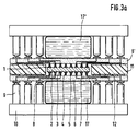
- Another way of equalizing unevenness consists in providing a pressure pad 17 in the form of a silicone sheath filled with liquid or gas (see Fig. 3).
- this gap should be filled by a pressure pad 17 (see Fig. 3). This pad acts as a hold-down device since the translator foil could buckle at these places.
- test arrangements according to Figures 1a, b, c and d comprise:
- Fig. 1a shows an embodiment of the invention in which a probe adapter is arranged on one side of the test specimen 2 and on the other side there is a translator foil.
- Fig. 1b is a magnification of the bump on the translator foil of Fig. 1a.
- a hemisphere 4a made from nickel or another metal, whose surface can also be oval-shaped, has been deposited.
- Onto this layer a layer of gold or other metal 4b is additionally deposited.
- Figure 1c shows an embodiment in which a probe adapter is arranged on one side of the test specimen 2 and, on the other side, a translator foil and a rubber layer 18 which becomes electrically conductive when depressed are arranged.
- the assumption is made that the contact areas 3 of printed circuit board 2 are staggered in height or that the printed circuit board is uneven. In this case the uneven areas are to be equalized and a contact ensured by using a rubber layer 18, which is conductive when depressed, next to the pressure pad 17.
- the rubber layer is not conductive if not depressed and begins to conduct when subjected to a minimum vertical pressure.
- Figure 1d shows an embodiment in which on one side of the test specimen 2 a probe adapter is arranged and on the other side a translator foil is arranged, with a vacuum established in the region of the test specimen.
- the contacts of the test specimen on the side facing a table 20 are tapped by bumps 4 and are expanded by the lower translator foil such that they can be bridged onto the upper translator foil by simple support layers 11 such as feed-through FR4 printed circuit boards or polyimide sheets having the pitch of the probes. This enables both sides of the board to be tested simultaneously using a one-sided probe adapter.
- the contacts on the upper side of the printed circuit board are similarly tapped by bumps and conducted in the correct pitch onto the outside of the translator foil to the test probes.
- test arrangements in Figures 2a, 2b comprise:
- the contact areas 1 and 3 of the test specimen 2 generally have different patterns.
- the patterns on the translator foils 6, 6' for the two sides also differ.
- Figure 2b depicts an embodiment with double-sided probe adapters, translator foils and rubber layers which become conductive when depressed, under vacuum.
- rubber layers 18, 18' which are electrically conductive when depressed have been inserted to equalize unevenness.
- the rubber layers become electrically conductive when subjected to a certain minimum pressure.
- the space between the translator foils is evacuated. This gives rise to a rigid package which permits very good contact with the probe adapter.
- Figures 3a, 3b describe electrical test fixtures in which multichip modules or printed circuit boards can be tested on test installations with double-sided probe adapters. Both sides of the printed circuit board are expanded, contacted and tested in a single step. This permits very fast electrical testing to be performed on complex printed circuit boards.
- test arrangements in Figures 3a, 3b comprise:
- the fixture according to Figures 3a, 3b differs from Figures 2a, 2b in that no vacuum is used in the first fixture.
- other measures must be used to ensure that when contacted by the probe adapters 9, 10 the bumps 4 of the translator foils 6 fit closely to the contact areas 1 of the test specimen. If not all of the probes of the adapter are now in use, i.e. if spaces arise between the foil and the adapter, these should be equalized by an additionally inserted pressure pad 17.
- This pressure pad consists of a silicone sheath filled with liquid or gas and acts as a hold-down device.
- electrically conductive rubber layers 18, 18' can be employed, which equalize the height variations. If not depressed the rubber layers are nonconductive and they begin to conduct when subjected to a certain minimum pressure.
- Figures 4a, 4b describe electrical test fixtures in which multichip modules or printed circuit boards can be tested on test installations with double-sided probe adapters. Both sides of the printed circuit board are expanded, contacted and tested in a single step.
- the use of multi-layer translator foils enables the expansion of the test specimen's surface to be adapted to a smaller probe grid. By evacuating the space between the translator foils a rigid package is obtained which permits very good contact with the probes of the test adapter. This fixture permits very fast electrical testing to be performed on complex printed circuit boards.
- electrically conductive rubber layers 18 can be employed which equalize the height variations. When not depressed the rubber layers are nonconductive and they begin to conduct when subjected to a certain minimum pressure.
Landscapes
- Physics & Mathematics (AREA)
- General Physics & Mathematics (AREA)
- Engineering & Computer Science (AREA)
- Computer Hardware Design (AREA)
- Microelectronics & Electronic Packaging (AREA)
- General Engineering & Computer Science (AREA)
- Testing Of Short-Circuits, Discontinuities, Leakage, Or Incorrect Line Connections (AREA)
- Measuring Leads Or Probes (AREA)
- Tests Of Electronic Circuits (AREA)
Applications Claiming Priority (2)
| Application Number | Priority Date | Filing Date | Title |
|---|---|---|---|
| DE19654404A DE19654404A1 (de) | 1996-12-24 | 1996-12-24 | Adaptationsvorrichtung zum elektrischen Test von Leiterplatten |
| DE19654404 | 1996-12-24 |
Publications (2)
| Publication Number | Publication Date |
|---|---|
| EP0851234A2 true EP0851234A2 (de) | 1998-07-01 |
| EP0851234A3 EP0851234A3 (de) | 1999-07-28 |
Family
ID=7816245
Family Applications (1)
| Application Number | Title | Priority Date | Filing Date |
|---|---|---|---|
| EP97120692A Withdrawn EP0851234A3 (de) | 1996-12-24 | 1997-11-26 | Anordnung zur elektrischen Prüfung von gedruckten Schaltungen |
Country Status (6)
| Country | Link |
|---|---|
| US (1) | US6147505A (de) |
| EP (1) | EP0851234A3 (de) |
| JP (1) | JPH10232260A (de) |
| KR (1) | KR19980064499A (de) |
| DE (1) | DE19654404A1 (de) |
| TW (1) | TW366423B (de) |
Cited By (1)
| Publication number | Priority date | Publication date | Assignee | Title |
|---|---|---|---|---|
| CN106443299A (zh) * | 2016-09-27 | 2017-02-22 | 惠州市金百泽电路科技有限公司 | 一种侦断印制电路板台阶孔开短路功能性缺陷的检测方法 |
Families Citing this family (29)
| Publication number | Priority date | Publication date | Assignee | Title |
|---|---|---|---|---|
| US20020053734A1 (en) | 1993-11-16 | 2002-05-09 | Formfactor, Inc. | Probe card assembly and kit, and methods of making same |
| US6483328B1 (en) | 1995-11-09 | 2002-11-19 | Formfactor, Inc. | Probe card for probing wafers with raised contact elements |
| US6114763A (en) * | 1997-05-30 | 2000-09-05 | Tessera, Inc. | Semiconductor package with translator for connection to an external substrate |
| WO2000017662A1 (de) * | 1998-09-24 | 2000-03-30 | Mci Computer Gmbh | Testvorrichtung für module |
| JP2000183483A (ja) * | 1998-12-21 | 2000-06-30 | Shinko Electric Ind Co Ltd | 電子部品の検査用基板及びその製造方法並びに電子部品の検査方法 |
| DE19939955A1 (de) | 1999-08-23 | 2001-03-01 | Atg Test Systems Gmbh | Prüfnadel für einen Rasteranpassungsadapter einer Vorrichtung zum Testen von Leiterplatten |
| DE19942891A1 (de) * | 1999-09-08 | 2001-05-10 | Volkswagen Ag | Verfahren zur Neutralisierung einer visuell nicht erkennbaren Markierung von Gegenständen |
| US6476629B1 (en) * | 2000-02-23 | 2002-11-05 | Micron Technology, Inc. | In-tray burn-in board for testing integrated circuit devices in situ on processing trays |
| JP4099412B2 (ja) * | 2003-03-19 | 2008-06-11 | 株式会社ルネサステクノロジ | 半導体集積回路装置の製造方法 |
| US7583513B2 (en) * | 2003-09-23 | 2009-09-01 | Intel Corporation | Apparatus for providing an integrated printed circuit board registration coupon |
| US20050253602A1 (en) * | 2004-04-28 | 2005-11-17 | Cram Daniel P | Resilient contact probe apparatus, methods of using and making, and resilient contact probes |
| WO2006087877A1 (ja) * | 2005-02-16 | 2006-08-24 | Jsr Corporation | 複合導電性シートおよびその製造方法、異方導電性コネクター、アダプター装置並びに回路装置の電気的検査装置 |
| US7307437B1 (en) * | 2005-03-24 | 2007-12-11 | Hewlett-Packard Development Company, L.P. | Arrangement with conductive pad embedment |
| US7385408B1 (en) | 2005-07-12 | 2008-06-10 | Amkor Technology, Inc. | Apparatus and method for testing integrated circuit devices having contacts on multiple surfaces |
| US7511510B2 (en) * | 2005-11-30 | 2009-03-31 | International Business Machines Corporation | Nanoscale fault isolation and measurement system |
| TWI600099B (zh) * | 2006-07-07 | 2017-09-21 | 川斯拉利特公司 | 平面延伸電導體超越基材邊緣的方法和設備 |
| DE102007032557B4 (de) | 2007-07-12 | 2010-09-16 | Multitest Elektronische Systeme Gmbh | Vorrichtung zum Testen von elektronischen Bauelementen, insbesondere IC's, mit innerhalb einer Drucktestkammer angeordnetem Abdichtboard |
| DE102007047269A1 (de) * | 2007-10-02 | 2009-04-09 | Atg Luther & Maelzer Gmbh | Vollrasterkassette für einen Paralleltester zum Testen einer unbestückten Leiterplatte, Federkontaktstift für eine solche Vollrasterkassette sowie Adapter für einen Paralleltester zum Testen einer unbestückten Leiterplatte |
| JP5164543B2 (ja) * | 2007-12-05 | 2013-03-21 | 東京エレクトロン株式会社 | プローブカードの製造方法 |
| EP2131204B1 (de) * | 2008-06-06 | 2012-11-14 | Texas Instruments France | Verfahren und System zum Prüfen einer Halbleiterverpackung |
| TWI416121B (zh) * | 2009-11-04 | 2013-11-21 | Mjc Probe Inc | 探針卡 |
| AT12317U1 (de) * | 2010-04-13 | 2012-03-15 | Austria Tech & System Tech | Verfahren zur integration eines elektronischen bauteils in eine leiterplatte sowie leiterplatte mit einem darin integrierten elektronischen bauteil |
| CN102478593B (zh) * | 2010-11-30 | 2014-04-16 | 励威电子股份有限公司 | 探针卡结构 |
| US9204537B2 (en) * | 2012-09-20 | 2015-12-01 | Finisar Corporation | High-speed pluggable rigid-end flex circuit |
| CN104155563B (zh) * | 2014-08-26 | 2018-02-02 | 昆山迈致治具科技有限公司 | 一种电路板的测试治具 |
| JP6223317B2 (ja) * | 2014-11-14 | 2017-11-01 | 三菱電機株式会社 | 半導体検査装置および半導体検査方法 |
| KR102688319B1 (ko) | 2019-09-30 | 2024-07-24 | 미쓰비시덴키 가부시키가이샤 | 검사 지그 |
| CN111600150B (zh) * | 2020-05-29 | 2021-09-28 | 东莞华贝电子科技有限公司 | 卡槽转换器、电路板组件及电子设备 |
| JP2026003513A (ja) * | 2024-06-24 | 2026-01-13 | 株式会社 東京ウエルズ | ワーク検査装置 |
Family Cites Families (20)
| Publication number | Priority date | Publication date | Assignee | Title |
|---|---|---|---|---|
| US3654585A (en) * | 1970-03-11 | 1972-04-04 | Brooks Research And Mfg Inc | Coordinate conversion for the testing of printed circuit boards |
| DE3031137A1 (de) * | 1980-08-18 | 1982-03-04 | Siemens AG, 1000 Berlin und 8000 München | Vorrichtung zum pruefen einer elektrischen leiterplatte |
| US4443756A (en) * | 1980-11-25 | 1984-04-17 | Lightbody James D | Apparatus and method for testing circuit boards |
| US4528500A (en) * | 1980-11-25 | 1985-07-09 | Lightbody James D | Apparatus and method for testing circuit boards |
| US4571542A (en) * | 1982-06-30 | 1986-02-18 | Japan Synthetic Rubber Co., Ltd. | Method and unit for inspecting printed wiring boards |
| DE3229448C2 (de) * | 1982-08-06 | 1987-04-23 | Siemens AG, 1000 Berlin und 8000 München | Vakuumadapter zur Prüfung von Flachbaugruppen |
| US4538104A (en) * | 1983-04-11 | 1985-08-27 | Test Point 1, Inc. | In-circuit test apparatus for printed circuit board |
| US4724383A (en) * | 1985-05-03 | 1988-02-09 | Testsystems, Inc. | PC board test fixture |
| DE8617408U1 (de) * | 1986-06-30 | 1986-08-21 | Siemens AG, 1000 Berlin und 8000 München | Kontaktiervorrichtung für zu prüfende Bauelemente der Mikroelektronik |
| DE3639360A1 (de) * | 1986-11-18 | 1988-05-19 | Luther Erich | Pruefstift fuer einen adapter zum verbinden von im raster befindlichen pruefkontakten eines leiterplattenpruefgeraetes mit in und/oder ausser raster befindlichen pruefpunkten eines prueflings |
| US4870354A (en) * | 1988-08-11 | 1989-09-26 | Zehntel, Inc. | Apparatus for contacting a printed circuit board with an array of test probes |
| DE3838413A1 (de) * | 1988-11-12 | 1990-05-17 | Mania Gmbh | Adapter fuer elektronische pruefvorrichtungen fuer leiterplatten und dergl. |
| US4977370A (en) * | 1988-12-06 | 1990-12-11 | Genrad, Inc. | Apparatus and method for circuit board testing |
| US5012187A (en) * | 1989-11-03 | 1991-04-30 | Motorola, Inc. | Method for parallel testing of semiconductor devices |
| US5225037A (en) * | 1991-06-04 | 1993-07-06 | Texas Instruments Incorporated | Method for fabrication of probe card for testing of semiconductor devices |
| US5574382A (en) * | 1991-09-17 | 1996-11-12 | Japan Synthetic Rubber Co., Ltd. | Inspection electrode unit for printed wiring board |
| KR0140034B1 (ko) * | 1993-12-16 | 1998-07-15 | 모리시다 요이치 | 반도체 웨이퍼 수납기, 반도체 웨이퍼의 검사용 집적회로 단자와 프로브 단자와의 접속방법 및 그 장치, 반도체 집적회로의 검사방법, 프로브카드 및 그 제조방법 |
| US5506510A (en) * | 1994-05-18 | 1996-04-09 | Genrad, Inc. | Adaptive alignment probe fixture for circuit board tester |
| US5629630A (en) * | 1995-02-27 | 1997-05-13 | Motorola, Inc. | Semiconductor wafer contact system and method for contacting a semiconductor wafer |
| US5926029A (en) * | 1997-05-27 | 1999-07-20 | International Business Machines Corporation | Ultra fine probe contacts |
-
1996
- 1996-12-24 DE DE19654404A patent/DE19654404A1/de not_active Withdrawn
-
1997
- 1997-11-26 EP EP97120692A patent/EP0851234A3/de not_active Withdrawn
- 1997-12-23 KR KR1019970072439A patent/KR19980064499A/ko not_active Ceased
- 1997-12-23 TW TW086119610A patent/TW366423B/zh active
- 1997-12-23 US US08/997,008 patent/US6147505A/en not_active Expired - Lifetime
- 1997-12-24 JP JP9354853A patent/JPH10232260A/ja active Pending
Cited By (2)
| Publication number | Priority date | Publication date | Assignee | Title |
|---|---|---|---|---|
| CN106443299A (zh) * | 2016-09-27 | 2017-02-22 | 惠州市金百泽电路科技有限公司 | 一种侦断印制电路板台阶孔开短路功能性缺陷的检测方法 |
| CN106443299B (zh) * | 2016-09-27 | 2019-01-04 | 惠州市金百泽电路科技有限公司 | 一种侦断印制电路板台阶孔开短路功能性缺陷的检测方法 |
Also Published As
| Publication number | Publication date |
|---|---|
| DE19654404A1 (de) | 1998-06-25 |
| KR19980064499A (ko) | 1998-10-07 |
| US6147505A (en) | 2000-11-14 |
| JPH10232260A (ja) | 1998-09-02 |
| EP0851234A3 (de) | 1999-07-28 |
| TW366423B (en) | 1999-08-11 |
Similar Documents
| Publication | Publication Date | Title |
|---|---|---|
| US6147505A (en) | Adapter arrangement for electrically testing printed circuit boards | |
| US5915977A (en) | System and interconnect for making temporary electrical connections with bumped semiconductor components | |
| US6310484B1 (en) | Semiconductor test interconnect with variable flexure contacts | |
| US6952054B2 (en) | Semiconductor package having interconnect with conductive members | |
| US6242935B1 (en) | Interconnect for testing semiconductor components and method of fabrication | |
| KR100399210B1 (ko) | 탐침 카드 조립체 | |
| US7409762B2 (en) | Method for fabricating an interconnect for semiconductor components | |
| US6297658B1 (en) | Wafer burn-in cassette and method of manufacturing probe card for use therein | |
| JP4709850B2 (ja) | 電気的接続デバイス及びこれの製造方法 | |
| KR20090108608A (ko) | 회전형 접촉 요소 및 이 회전형 접촉 요소의 제조 방법 | |
| US20020048973A1 (en) | Contact structure and production method thereof and probe contact assembly using same | |
| JPH10227826A (ja) | プリント回路基板の試験装置及びその方法 | |
| EP0171232A2 (de) | Band für die Anschweissung von Flächen | |
| US6891360B1 (en) | Plated probe structure | |
| JPH09105761A (ja) | プローブ構造の製造方法およびそれに用いられる回路基板 | |
| EP1292429A1 (de) | Sauggreifer mit elektrischen prüfpunkten | |
| US6303988B1 (en) | Wafer scale burn-in socket | |
| US5880591A (en) | System for circuit modules having a plurality of independently positionable probes | |
| KR101047009B1 (ko) | 프로브용 기판 제조방법 | |
| TW202611522A (zh) | 介面裝置及自動試驗裝置 | |
| JPH08327689A (ja) | コネクタおよびそれを用いる半導体検査方法ならびに装置 | |
| JPH03237369A (ja) | テストヘッド構造 | |
| JPH09266357A (ja) | エレクトリカルテスト用配線基板及びその製造法 | |
| JP2006332697A (ja) | エレクトリカルテスト用配線基板及びその製造法 |
Legal Events
| Date | Code | Title | Description |
|---|---|---|---|
| PUAI | Public reference made under article 153(3) epc to a published international application that has entered the european phase |
Free format text: ORIGINAL CODE: 0009012 |
|
| AK | Designated contracting states |
Kind code of ref document: A2 Designated state(s): DE FI FR GB IT SE |
|
| AX | Request for extension of the european patent |
Free format text: AL;LT;LV;MK;RO;SI |
|
| PUAL | Search report despatched |
Free format text: ORIGINAL CODE: 0009013 |
|
| AK | Designated contracting states |
Kind code of ref document: A3 Designated state(s): AT BE CH DE DK ES FI FR GB GR IE IT LI LU MC NL PT SE |
|
| AX | Request for extension of the european patent |
Free format text: AL;LT;LV;MK;RO;SI |
|
| 17P | Request for examination filed |
Effective date: 19990630 |
|
| AKX | Designation fees paid |
Free format text: DE FI FR GB IT SE |
|
| RAP1 | Party data changed (applicant data changed or rights of an application transferred) |
Owner name: HEWLETT-PACKARD COMPANY, A DELAWARE CORPORATION |
|
| 17Q | First examination report despatched |
Effective date: 20041020 |
|
| STAA | Information on the status of an ep patent application or granted ep patent |
Free format text: STATUS: THE APPLICATION IS DEEMED TO BE WITHDRAWN |
|
| 18D | Application deemed to be withdrawn |
Effective date: 20060328 |