EP0851332A2 - Spannungsregler - Google Patents
Spannungsregler Download PDFInfo
- Publication number
- EP0851332A2 EP0851332A2 EP97310344A EP97310344A EP0851332A2 EP 0851332 A2 EP0851332 A2 EP 0851332A2 EP 97310344 A EP97310344 A EP 97310344A EP 97310344 A EP97310344 A EP 97310344A EP 0851332 A2 EP0851332 A2 EP 0851332A2
- Authority
- EP
- European Patent Office
- Prior art keywords
- transistor
- coupled
- control region
- amplifier
- source follower
- Prior art date
- Legal status (The legal status is an assumption and is not a legal conclusion. Google has not performed a legal analysis and makes no representation as to the accuracy of the status listed.)
- Granted
Links
Images
Classifications
-
- G—PHYSICS
- G05—CONTROLLING; REGULATING
- G05F—SYSTEMS FOR REGULATING ELECTRIC OR MAGNETIC VARIABLES
- G05F3/00—Non-retroactive systems for regulating electric variables by using an uncontrolled element, or an uncontrolled combination of elements, such element or such combination having self-regulating properties
- G05F3/02—Regulating voltage or current
- G05F3/08—Regulating voltage or current wherein the variable is DC
- G05F3/10—Regulating voltage or current wherein the variable is DC using uncontrolled devices with non-linear characteristics
- G05F3/16—Regulating voltage or current wherein the variable is DC using uncontrolled devices with non-linear characteristics being semiconductor devices
- G05F3/20—Regulating voltage or current wherein the variable is DC using uncontrolled devices with non-linear characteristics being semiconductor devices using diode- transistor combinations
- G05F3/24—Regulating voltage or current wherein the variable is DC using uncontrolled devices with non-linear characteristics being semiconductor devices using diode- transistor combinations wherein the transistors are of the field-effect type only
- G05F3/242—Regulating voltage or current wherein the variable is DC using uncontrolled devices with non-linear characteristics being semiconductor devices using diode- transistor combinations wherein the transistors are of the field-effect type only with compensation for device parameters, e.g. channel width modulation, threshold voltage, processing, or external variations, e.g. temperature, loading, supply voltage
-
- H—ELECTRICITY
- H03—ELECTRONIC CIRCUITRY
- H03G—CONTROL OF AMPLIFICATION
- H03G1/00—Details of arrangements for controlling amplification
- H03G1/0005—Circuits characterised by the type of controlling devices operated by a controlling current or voltage signal
-
- G—PHYSICS
- G05—CONTROLLING; REGULATING
- G05F—SYSTEMS FOR REGULATING ELECTRIC OR MAGNETIC VARIABLES
- G05F3/00—Non-retroactive systems for regulating electric variables by using an uncontrolled element, or an uncontrolled combination of elements, such element or such combination having self-regulating properties
- G05F3/02—Regulating voltage or current
- G05F3/08—Regulating voltage or current wherein the variable is DC
- G05F3/10—Regulating voltage or current wherein the variable is DC using uncontrolled devices with non-linear characteristics
- G05F3/16—Regulating voltage or current wherein the variable is DC using uncontrolled devices with non-linear characteristics being semiconductor devices
- G05F3/20—Regulating voltage or current wherein the variable is DC using uncontrolled devices with non-linear characteristics being semiconductor devices using diode- transistor combinations
- G05F3/26—Current mirrors
- G05F3/267—Current mirrors using both bipolar and field-effect technology
Definitions
- This invention generally relates to electronic systems and in particular it relates to voltage regulators.
- the function of a voltage regulator is to take a varying input voltage supply and generate a stable output voltage.
- the efficiency of modern power supply systems, especially battery operated ones, is directly related to the useable operating voltage and current over head required by the system's voltage regulator.
- the useable operating voltage is called the "drop-out" voltage, which is the difference between the input and output voltages of the regulator while the regulator still maintains regulation. The smaller this difference, the more efficient the system.
- batteries can supply only a finite amount of charge, so the more quiescent current the regulator uses (which is wasted current as far as the system is concerned), the less life the battery will have and therefore the system will be less efficient.
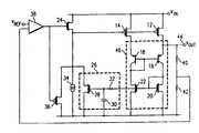
- the voltage regulator circuit includes: a first MOS transistor connected between a voltage supply line and an output node, the first MOS transistor being arranged for providing a stable voltage on the output node; a source follower coupled to a gate of the first MOS transistor; an amplifier coupled to a gate of the source follower for controlling the response of the first MOS transistor; negative feedback circuitry coupled between the output node and the amplifier, the feedback circuitry being arranged for providing feedback to the amplifier; a current conveyer coupled to the first MOS transistor; and positive feedback circuitry coupled between the current conveyer and the source follower.
- a circuit diagram of a low drop-out (LDO) voltage regulator with PMOS pass element is illustrated.
- the circuit includes PMOS pass device 12 (PMOS transistor); PMOS transistor 14; PNP transistors 16 and 18; NMOS transistors 20 and 22; NMOS transistor 24; positive feedback circuit 26 which includes NMOS transistor 28, capacitor 30, and resistor 32; current source 34; PMOS transistor 36; error amplifier 38 (operational amplifier), resistors 40 and 42, voltage reference V REF , output voltage V OUT , and input voltage V IN .
- the output voltage V OUT is regulated by pass transistor 12.
- the error amp 38 which is an operational amplifier, controls transistor 12 through transistor 24.
- the input voltage V IN changes or the current being drawn from an external load at node 44 changes
- the output voltage V OUT begins to change causing the voltage across the second resistor 42 to change.
- the error amp 38 then adjusts the gate voltage of transistor 24 so that the output voltage V OUT is maintained in the desired range.
- Current mirror transistor 14 monitors the current of transistor 12.
- the ratio of transistor 14 to transistor 12 is such that the current in transistor 14 is only a small fraction of the current in transistor 12 (for example 1:1000).
- PNP transistors 16 and 18 together with NMOS transistors 20 and 22 form a current conveyor 46 which forces the current in PNP transistors 20 and 22 to be the same.
- the current conveyor ensures that the V DS and V GS of transistors 12 and 14 are the same. Since the V GS of transistors 12 and 14 are the same, the currents in PNP transistors 16 and 18 are the same.
- the current in the current conveyor 46 is equal to the current in transistor 14.
- Transistor 28 is larger than transistors 20 and 22 in order to provide sufficient current for the source follower transistor 24 which drives output transistor 12.
- Transistor 24 is an isolated natural NMOS with a low V T .
- Resistor 32 and capacitor 30 provide frequency compensation for the positive feedback to make sure the positive feedback never overcomes the negative feedback so that the circuit does not oscillate.
- the current conveyor performs two functions. First, it ensures that the external pole and the internal pole remain separated for stability. Second, the positive feedback improves the load regulation by modulating the V GS of transistor 24 proportionately with the V GS of transistor 12. This compensates the output impedance of the circuit.
- current source 34 pulls on transistor 24 so that the circuit works where there is no load at output node 44.
- current source 34 provides only a small current on the order of one micro amp. With this small current, the power consumption of the circuit will be extremely small when there is no load on the output. This is an important feature for battery powered devices.
- Transistor 36 is used to enhance the slew rate of the circuit. Transistor 36 allows the circuit to come back into regulation quickly when there is a rapid change in load. Transistor 36 turns on and helps the transient response when going from no load at output node 44 to a full load or some load condition at node 44.
Landscapes
- Engineering & Computer Science (AREA)
- Physics & Mathematics (AREA)
- Microelectronics & Electronic Packaging (AREA)
- Nonlinear Science (AREA)
- Electromagnetism (AREA)
- General Physics & Mathematics (AREA)
- Radar, Positioning & Navigation (AREA)
- Automation & Control Theory (AREA)
- Continuous-Control Power Sources That Use Transistors (AREA)
- Amplifiers (AREA)
Applications Claiming Priority (2)
| Application Number | Priority Date | Filing Date | Title |
|---|---|---|---|
| US3367996P | 1996-12-19 | 1996-12-19 | |
| US33679P | 1996-12-19 |
Publications (3)
| Publication Number | Publication Date |
|---|---|
| EP0851332A2 true EP0851332A2 (de) | 1998-07-01 |
| EP0851332A3 EP0851332A3 (de) | 1999-03-24 |
| EP0851332B1 EP0851332B1 (de) | 2004-02-25 |
Family
ID=21871809
Family Applications (1)
| Application Number | Title | Priority Date | Filing Date |
|---|---|---|---|
| EP97310344A Expired - Lifetime EP0851332B1 (de) | 1996-12-19 | 1997-12-19 | Spannungsregler |
Country Status (6)
| Country | Link |
|---|---|
| US (1) | US5867015A (de) |
| EP (1) | EP0851332B1 (de) |
| JP (1) | JPH10187258A (de) |
| KR (1) | KR19980064252A (de) |
| DE (1) | DE69727783T2 (de) |
| TW (1) | TW357477B (de) |
Cited By (2)
| Publication number | Priority date | Publication date | Assignee | Title |
|---|---|---|---|---|
| EP0957421A3 (de) * | 1998-05-13 | 2000-03-15 | Texas Instruments Incorporated | Stromeffiziente Regelungseinichtung mit kleiner Verlustspannung, verbesserter Lasregelung und Frequenzgang |
| EP1280032A1 (de) * | 2001-07-26 | 2003-01-29 | Alcatel | Spannungsregler mit kleiner Verlustspannung |
Families Citing this family (66)
| Publication number | Priority date | Publication date | Assignee | Title |
|---|---|---|---|---|
| US5982226A (en) * | 1997-04-07 | 1999-11-09 | Texas Instruments Incorporated | Optimized frequency shaping circuit topologies for LDOs |
| SE520906C2 (sv) * | 1997-10-28 | 2003-09-09 | Ericsson Telefon Ab L M | Spänningsregulator med ett mycket lågt 'drop-out voltage' |
| US6285246B1 (en) * | 1998-09-15 | 2001-09-04 | California Micro Devices, Inc. | Low drop-out regulator capable of functioning in linear and saturated regions of output driver |
| US6329804B1 (en) | 1999-10-13 | 2001-12-11 | National Semiconductor Corporation | Slope and level trim DAC for voltage reference |
| US6201379B1 (en) | 1999-10-13 | 2001-03-13 | National Semiconductor Corporation | CMOS voltage reference with a nulling amplifier |
| US6218822B1 (en) | 1999-10-13 | 2001-04-17 | National Semiconductor Corporation | CMOS voltage reference with post-assembly curvature trim |
| US6198266B1 (en) | 1999-10-13 | 2001-03-06 | National Semiconductor Corporation | Low dropout voltage reference |
| US6812678B1 (en) * | 1999-11-18 | 2004-11-02 | Texas Instruments Incorporated | Voltage independent class A output stage speedup circuit |
| JP3540231B2 (ja) * | 2000-01-31 | 2004-07-07 | 沖電気工業株式会社 | クランプ回路及び非接触式通信用インターフェース回路 |
| US6359427B1 (en) * | 2000-08-04 | 2002-03-19 | Maxim Integrated Products, Inc. | Linear regulators with low dropout and high line regulation |
| US6333623B1 (en) | 2000-10-30 | 2001-12-25 | Texas Instruments Incorporated | Complementary follower output stage circuitry and method for low dropout voltage regulator |
| US6509727B2 (en) * | 2000-11-24 | 2003-01-21 | Texas Instruments Incorporated | Linear regulator enhancement technique |
| FR2818762B1 (fr) * | 2000-12-22 | 2003-04-04 | St Microelectronics Sa | Regulateur de tension a gain statique en boucle ouverte reduit |
| FR2819064B1 (fr) * | 2000-12-29 | 2003-04-04 | St Microelectronics Sa | Regulateur de tension a stabilite amelioree |
| US6535055B2 (en) * | 2001-03-19 | 2003-03-18 | Texas Instruments Incorporated | Pass device leakage current correction circuit for use in linear regulators |
| JP5021866B2 (ja) * | 2001-03-28 | 2012-09-12 | カウンシル オブ サイエンティフィク アンド インダストリアル リサーチ | 低電圧、低電力および高性能のii型電流コンベヤのための模擬回路レイアウト |
| US6971004B1 (en) | 2001-11-19 | 2005-11-29 | Cypress Semiconductor Corp. | System and method of dynamically reconfiguring a programmable integrated circuit |
| US6600362B1 (en) * | 2002-02-08 | 2003-07-29 | Toko, Inc. | Method and circuits for parallel sensing of current in a field effect transistor (FET) |
| US6639390B2 (en) * | 2002-04-01 | 2003-10-28 | Texas Instruments Incorporated | Protection circuit for miller compensated voltage regulators |
| US6819165B2 (en) * | 2002-05-30 | 2004-11-16 | Analog Devices, Inc. | Voltage regulator with dynamically boosted bias current |
| US6897715B2 (en) * | 2002-05-30 | 2005-05-24 | Analog Devices, Inc. | Multimode voltage regulator |
| US6979984B2 (en) * | 2003-04-14 | 2005-12-27 | Semiconductor Components Industries, L.L.C. | Method of forming a low quiescent current voltage regulator and structure therefor |
| US6879142B2 (en) * | 2003-08-20 | 2005-04-12 | Broadcom Corporation | Power management unit for use in portable applications |
| JP4263068B2 (ja) * | 2003-08-29 | 2009-05-13 | 株式会社リコー | 定電圧回路 |
| US7026802B2 (en) * | 2003-12-23 | 2006-04-11 | Cypress Semiconductor Corporation | Replica biased voltage regulator |
| US6975099B2 (en) | 2004-02-27 | 2005-12-13 | Texas Instruments Incorporated | Efficient frequency compensation for linear voltage regulators |
| ATE396444T1 (de) * | 2004-03-15 | 2008-06-15 | Freescale Semiconductor Inc | Gleichstromspannungsregler mit niedrigem spannungsabfall |
| US7205828B2 (en) * | 2004-08-02 | 2007-04-17 | Silicon Laboratories, Inc. | Voltage regulator having a compensated load conductance |
| US7218083B2 (en) * | 2005-02-25 | 2007-05-15 | O2Mincro, Inc. | Low drop-out voltage regulator with enhanced frequency compensation |
| US7656224B2 (en) * | 2005-03-16 | 2010-02-02 | Texas Instruments Incorporated | Power efficient dynamically biased buffer for low drop out regulators |
| JP4814556B2 (ja) * | 2005-06-24 | 2011-11-16 | Hoya株式会社 | レギュレータ回路 |
| WO2007073767A1 (en) * | 2005-12-23 | 2007-07-05 | Infineon Technologies Ag | Over-voltage and under voltage protection circuit |
| US7554152B1 (en) | 2006-01-11 | 2009-06-30 | National Semiconductor Corporation | Versatile system for integrated sense transistor |
| US8564252B2 (en) * | 2006-11-10 | 2013-10-22 | Cypress Semiconductor Corporation | Boost buffer aid for reference buffer |
| US8035401B2 (en) | 2007-04-18 | 2011-10-11 | Cypress Semiconductor Corporation | Self-calibrating driver for charging a capacitive load to a desired voltage |
| US9720805B1 (en) | 2007-04-25 | 2017-08-01 | Cypress Semiconductor Corporation | System and method for controlling a target device |
| CN100480944C (zh) * | 2007-05-15 | 2009-04-22 | 北京中星微电子有限公司 | 一种压控电流源及带有压控电流源的低压差稳压电源 |
| DE102007031054B4 (de) | 2007-07-04 | 2018-08-02 | Texas Instruments Deutschland Gmbh | Referenzspannungsgenerator mit Bootstrap-Effekt |
| JP4642827B2 (ja) * | 2007-10-22 | 2011-03-02 | 株式会社リコー | 定電圧電源装置 |
| IT1392263B1 (it) * | 2008-12-15 | 2012-02-22 | St Microelectronics Des & Appl | Regolatore lineare di tipo low-dropout e corrispondente procedimento |
| US8378652B2 (en) * | 2008-12-23 | 2013-02-19 | Texas Instruments Incorporated | Load transient response time of LDOs with NMOS outputs with a voltage controlled current source |
| US8148962B2 (en) | 2009-05-12 | 2012-04-03 | Sandisk Il Ltd. | Transient load voltage regulator |
| EP2256578A1 (de) * | 2009-05-15 | 2010-12-01 | STMicroelectronics (Grenoble 2) SAS | Low-dropout Spannungsregler mit niedrigem Ruhestrom |
| WO2012003597A1 (en) * | 2010-07-05 | 2012-01-12 | St-Ericsson Sa | Voltage regulator circuit |
| US8502514B2 (en) | 2010-09-10 | 2013-08-06 | Himax Technologies Limited | Voltage regulation circuit |
| TWI411902B (zh) * | 2010-09-27 | 2013-10-11 | Himax Tech Ltd | 電壓調節電路 |
| US8364870B2 (en) | 2010-09-30 | 2013-01-29 | Cypress Semiconductor Corporation | USB port connected to multiple USB compliant devices |
| US8344713B2 (en) * | 2011-01-11 | 2013-01-01 | Freescale Semiconductor, Inc. | LDO linear regulator with improved transient response |
| US9667240B2 (en) | 2011-12-02 | 2017-05-30 | Cypress Semiconductor Corporation | Systems and methods for starting up analog circuits |
| CN103383580B (zh) * | 2012-05-03 | 2015-07-15 | 三星半导体(中国)研究开发有限公司 | 自适应低压差线性稳压器 |
| US8878601B2 (en) * | 2012-05-31 | 2014-11-04 | Taiwan Semiconductor Manufacturing Company, Ltd. | Power supply circuit with positive and negative feedback loops |
| CN104253544B (zh) * | 2013-06-28 | 2017-06-06 | 比亚迪股份有限公司 | 一种开关电源控制芯片的补偿电路 |
| CN107741754B (zh) | 2014-01-02 | 2020-06-09 | 意法半导体研发(深圳)有限公司 | 用于内部电源的具有改善的负载瞬态性能的ldo调节器 |
| DE102015205359B4 (de) * | 2015-03-24 | 2018-01-25 | Dialog Semiconductor (Uk) Limited | Ruhestrombegrenzung für einen low-dropout-regler bei einer dropout-bedingung |
| US10128821B2 (en) * | 2016-11-15 | 2018-11-13 | Stmicroelectronics, Inc. | Low output impedance, high speed and high voltage generator for use in driving a capacitive load |
| JP6902917B2 (ja) * | 2017-04-25 | 2021-07-14 | 新日本無線株式会社 | 定電圧電源回路 |
| US10146240B1 (en) * | 2018-02-01 | 2018-12-04 | Apple Inc. | High current LDO voltage regulator with dynamic pre-regulator |
| JP7042658B2 (ja) * | 2018-03-15 | 2022-03-28 | エイブリック株式会社 | ボルテージレギュレータ |
| US11287839B2 (en) * | 2019-09-25 | 2022-03-29 | Apple Inc. | Dual loop LDO voltage regulator |
| US11671081B2 (en) * | 2019-12-13 | 2023-06-06 | Qualcomm Incorporated | Rail-to-rail source follower buffer for switching regulator driver supply |
| CN114822640A (zh) | 2021-01-28 | 2022-07-29 | 威比特纳诺有限公司 | 用于电阻式随机存取存储器编程的电流和电压限制电路 |
| US12105548B2 (en) * | 2021-06-10 | 2024-10-01 | Texas Instruments Incorporated | Improving power supply rejection ratio across load and supply variances |
| US20240103550A1 (en) * | 2022-09-22 | 2024-03-28 | Apple Inc. | Low-dropout regulator with improved gain bandwidth and bias generation |
| CN116400769B (zh) * | 2023-04-04 | 2026-03-24 | 深圳市创芯微微电子有限公司 | 功耗控制电路、低压差线性稳压芯片和电子设备 |
| US20260023403A1 (en) * | 2024-07-16 | 2026-01-22 | Stmicroelectronics International N.V. | Fast recovery voltage regulator |
| EP4752673A1 (de) * | 2024-11-29 | 2026-06-03 | NXP USA, Inc. | Stromspiegel, gatetreiber und verfahren zur steuerung eines ausgangsstroms |
Family Cites Families (5)
| Publication number | Priority date | Publication date | Assignee | Title |
|---|---|---|---|---|
| US4779037A (en) * | 1987-11-17 | 1988-10-18 | National Semiconductor Corporation | Dual input low dropout voltage regulator |
| US4954769A (en) * | 1989-02-08 | 1990-09-04 | Burr-Brown Corporation | CMOS voltage reference and buffer circuit |
| JP3274306B2 (ja) * | 1995-01-20 | 2002-04-15 | 株式会社東芝 | 半導体集積回路装置 |
| EP0733959B1 (de) * | 1995-03-24 | 2001-06-13 | Co.Ri.M.Me. Consorzio Per La Ricerca Sulla Microelettronica Nel Mezzogiorno | Schaltungsanordnung zur Erzeugung einer Referenzspannung und Detektion eines Versorgungsspannungsabfalls und zugehöriges Verfahren |
| US5637992A (en) * | 1995-05-31 | 1997-06-10 | Sgs-Thomson Microelectronics, Inc. | Voltage regulator with load pole stabilization |
-
1997
- 1997-12-17 KR KR1019970069929A patent/KR19980064252A/ko not_active Withdrawn
- 1997-12-17 US US08/992,706 patent/US5867015A/en not_active Expired - Lifetime
- 1997-12-19 EP EP97310344A patent/EP0851332B1/de not_active Expired - Lifetime
- 1997-12-19 JP JP9351612A patent/JPH10187258A/ja active Pending
- 1997-12-19 DE DE69727783T patent/DE69727783T2/de not_active Expired - Lifetime
-
1998
- 1998-03-02 TW TW086119247A patent/TW357477B/zh not_active IP Right Cessation
Cited By (2)
| Publication number | Priority date | Publication date | Assignee | Title |
|---|---|---|---|---|
| EP0957421A3 (de) * | 1998-05-13 | 2000-03-15 | Texas Instruments Incorporated | Stromeffiziente Regelungseinichtung mit kleiner Verlustspannung, verbesserter Lasregelung und Frequenzgang |
| EP1280032A1 (de) * | 2001-07-26 | 2003-01-29 | Alcatel | Spannungsregler mit kleiner Verlustspannung |
Also Published As
| Publication number | Publication date |
|---|---|
| US5867015A (en) | 1999-02-02 |
| JPH10187258A (ja) | 1998-07-14 |
| EP0851332B1 (de) | 2004-02-25 |
| DE69727783T2 (de) | 2004-12-30 |
| DE69727783D1 (de) | 2004-04-01 |
| KR19980064252A (ko) | 1998-10-07 |
| TW357477B (en) | 1999-05-01 |
| EP0851332A3 (de) | 1999-03-24 |
Similar Documents
| Publication | Publication Date | Title |
|---|---|---|
| US5867015A (en) | Low drop-out voltage regulator with PMOS pass element | |
| US5625278A (en) | Ultra-low drop-out monolithic voltage regulator | |
| EP1365302B1 (de) | Spannungsregulierungseinrichtung mit niedrigem Spannungsabfall | |
| CN106558987B (zh) | 低静态电流线性调节器电路 | |
| US5672959A (en) | Low drop-out voltage regulator having high ripple rejection and low power consumption | |
| CN115777089B (zh) | 用于低压应用的低压差稳压器 | |
| EP0715238B1 (de) | Schaltung und Verfahren zur Spannungsregelung | |
| US6388433B2 (en) | Linear regulator with low overshooting in transient state | |
| US6856124B2 (en) | LDO regulator with wide output load range and fast internal loop | |
| US6573694B2 (en) | Stable low dropout, low impedance driver for linear regulators | |
| US8917069B2 (en) | Low drop-out voltage regulator with dynamic voltage control | |
| EP0846996B1 (de) | Leistungstransistorsteuerschaltung für Spannungsregler | |
| US20040046532A1 (en) | Low dropout voltage regulator using a depletion pass transistor | |
| EP2354881A1 (de) | Dominospannungsregler | |
| CN205092772U (zh) | 线性调节器控制电路 | |
| EP3594772B1 (de) | Spannungsregler mit geringem spannungsabfall, versorgungsspannungsschaltung und verfahren zum erzeugen einer sauberen versorgungsspannung | |
| US5929616A (en) | Device for voltage regulation with a low internal dissipation of energy | |
| WO2007035724A2 (en) | Soft-start circuit and method for power-up of an amplifier circuit | |
| EP0957421A3 (de) | Stromeffiziente Regelungseinichtung mit kleiner Verlustspannung, verbesserter Lasregelung und Frequenzgang | |
| US20080265856A1 (en) | Constant-voltage power circuit | |
| EP2430507A1 (de) | Spannungsregler mit transienter last | |
| US5909109A (en) | Voltage regulator predriver circuit | |
| KR970703555A (ko) | 전압 조절기(Voltage regulator) | |
| EP1280032A1 (de) | Spannungsregler mit kleiner Verlustspannung | |
| CN117590887B (zh) | 一种降低压降状态静态功耗的电路 |
Legal Events
| Date | Code | Title | Description |
|---|---|---|---|
| PUAI | Public reference made under article 153(3) epc to a published international application that has entered the european phase |
Free format text: ORIGINAL CODE: 0009012 |
|
| AK | Designated contracting states |
Kind code of ref document: A2 Designated state(s): DE FR GB IT NL |
|
| AX | Request for extension of the european patent |
Free format text: AL;LT;LV;RO;SI |
|
| PUAL | Search report despatched |
Free format text: ORIGINAL CODE: 0009013 |
|
| AK | Designated contracting states |
Kind code of ref document: A3 Designated state(s): AT BE CH DE DK ES FI FR GB GR IE IT LI LU MC NL PT SE |
|
| AX | Request for extension of the european patent |
Free format text: AL;LT;LV;RO;SI |
|
| 17P | Request for examination filed |
Effective date: 19990826 |
|
| 17Q | First examination report despatched |
Effective date: 19991020 |
|
| AKX | Designation fees paid |
Free format text: DE FR GB IT NL |
|
| GRAP | Despatch of communication of intention to grant a patent |
Free format text: ORIGINAL CODE: EPIDOSNIGR1 |
|
| GRAS | Grant fee paid |
Free format text: ORIGINAL CODE: EPIDOSNIGR3 |
|
| GRAA | (expected) grant |
Free format text: ORIGINAL CODE: 0009210 |
|
| AK | Designated contracting states |
Kind code of ref document: B1 Designated state(s): DE FR GB IT NL |
|
| PG25 | Lapsed in a contracting state [announced via postgrant information from national office to epo] |
Ref country code: NL Free format text: LAPSE BECAUSE OF FAILURE TO SUBMIT A TRANSLATION OF THE DESCRIPTION OR TO PAY THE FEE WITHIN THE PRESCRIBED TIME-LIMIT Effective date: 20040225 Ref country code: IT Free format text: LAPSE BECAUSE OF FAILURE TO SUBMIT A TRANSLATION OF THE DESCRIPTION OR TO PAY THE FEE WITHIN THE PRESCRIBED TIME-LIMIT;WARNING: LAPSES OF ITALIAN PATENTS WITH EFFECTIVE DATE BEFORE 2007 MAY HAVE OCCURRED AT ANY TIME BEFORE 2007. THE CORRECT EFFECTIVE DATE MAY BE DIFFERENT FROM THE ONE RECORDED. Effective date: 20040225 Ref country code: FR Free format text: LAPSE BECAUSE OF FAILURE TO SUBMIT A TRANSLATION OF THE DESCRIPTION OR TO PAY THE FEE WITHIN THE PRESCRIBED TIME-LIMIT Effective date: 20040225 |
|
| REG | Reference to a national code |
Ref country code: GB Ref legal event code: FG4D |
|
| REF | Corresponds to: |
Ref document number: 69727783 Country of ref document: DE Date of ref document: 20040401 Kind code of ref document: P |
|
| NLV1 | Nl: lapsed or annulled due to failure to fulfill the requirements of art. 29p and 29m of the patents act | ||
| PLBE | No opposition filed within time limit |
Free format text: ORIGINAL CODE: 0009261 |
|
| STAA | Information on the status of an ep patent application or granted ep patent |
Free format text: STATUS: NO OPPOSITION FILED WITHIN TIME LIMIT |
|
| EN | Fr: translation not filed | ||
| 26N | No opposition filed |
Effective date: 20041126 |
|
| PGFP | Annual fee paid to national office [announced via postgrant information from national office to epo] |
Ref country code: GB Payment date: 20121128 Year of fee payment: 16 |
|
| PGFP | Annual fee paid to national office [announced via postgrant information from national office to epo] |
Ref country code: DE Payment date: 20121221 Year of fee payment: 16 |
|
| REG | Reference to a national code |
Ref country code: DE Ref legal event code: R119 Ref document number: 69727783 Country of ref document: DE |
|
| GBPC | Gb: european patent ceased through non-payment of renewal fee |
Effective date: 20131219 |
|
| REG | Reference to a national code |
Ref country code: DE Ref legal event code: R119 Ref document number: 69727783 Country of ref document: DE Effective date: 20140701 |
|
| PG25 | Lapsed in a contracting state [announced via postgrant information from national office to epo] |
Ref country code: DE Free format text: LAPSE BECAUSE OF NON-PAYMENT OF DUE FEES Effective date: 20140701 |
|
| PG25 | Lapsed in a contracting state [announced via postgrant information from national office to epo] |
Ref country code: GB Free format text: LAPSE BECAUSE OF NON-PAYMENT OF DUE FEES Effective date: 20131219 |