EP0851481A2 - Procédé de fabrication d'un conducteur métallique encapsulé pour interconnexion multi-couche - Google Patents
Procédé de fabrication d'un conducteur métallique encapsulé pour interconnexion multi-couche Download PDFInfo
- Publication number
- EP0851481A2 EP0851481A2 EP97204012A EP97204012A EP0851481A2 EP 0851481 A2 EP0851481 A2 EP 0851481A2 EP 97204012 A EP97204012 A EP 97204012A EP 97204012 A EP97204012 A EP 97204012A EP 0851481 A2 EP0851481 A2 EP 0851481A2
- Authority
- EP
- European Patent Office
- Prior art keywords
- layer
- electrically conductive
- conductive metal
- lead
- metal layer
- Prior art date
- Legal status (The legal status is an assumption and is not a legal conclusion. Google has not performed a legal analysis and makes no representation as to the accuracy of the status listed.)
- Withdrawn
Links
Images
Classifications
-
- H—ELECTRICITY
- H10—SEMICONDUCTOR DEVICES; ELECTRIC SOLID-STATE DEVICES NOT OTHERWISE PROVIDED FOR
- H10W—GENERIC PACKAGES, INTERCONNECTIONS, CONNECTORS OR OTHER CONSTRUCTIONAL DETAILS OF DEVICES COVERED BY CLASS H10
- H10W20/00—Interconnections in chips, wafers or substrates
- H10W20/01—Manufacture or treatment
- H10W20/031—Manufacture or treatment of conductive parts of the interconnections
- H10W20/064—Manufacture or treatment of conductive parts of the interconnections by modifying the conductivity of conductive parts, e.g. by alloying
-
- H—ELECTRICITY
- H10—SEMICONDUCTOR DEVICES; ELECTRIC SOLID-STATE DEVICES NOT OTHERWISE PROVIDED FOR
- H10W—GENERIC PACKAGES, INTERCONNECTIONS, CONNECTORS OR OTHER CONSTRUCTIONAL DETAILS OF DEVICES COVERED BY CLASS H10
- H10W20/00—Interconnections in chips, wafers or substrates
- H10W20/01—Manufacture or treatment
- H10W20/031—Manufacture or treatment of conductive parts of the interconnections
- H10W20/056—Manufacture or treatment of conductive parts of the interconnections by filling conductive material into holes, grooves or trenches
-
- H—ELECTRICITY
- H10—SEMICONDUCTOR DEVICES; ELECTRIC SOLID-STATE DEVICES NOT OTHERWISE PROVIDED FOR
- H10W—GENERIC PACKAGES, INTERCONNECTIONS, CONNECTORS OR OTHER CONSTRUCTIONAL DETAILS OF DEVICES COVERED BY CLASS H10
- H10W20/00—Interconnections in chips, wafers or substrates
- H10W20/01—Manufacture or treatment
- H10W20/071—Manufacture or treatment of dielectric parts thereof
- H10W20/081—Manufacture or treatment of dielectric parts thereof by forming openings in the dielectric parts
-
- H—ELECTRICITY
- H10—SEMICONDUCTOR DEVICES; ELECTRIC SOLID-STATE DEVICES NOT OTHERWISE PROVIDED FOR
- H10W—GENERIC PACKAGES, INTERCONNECTIONS, CONNECTORS OR OTHER CONSTRUCTIONAL DETAILS OF DEVICES COVERED BY CLASS H10
- H10W20/00—Interconnections in chips, wafers or substrates
- H10W20/40—Interconnections external to wafers or substrates, e.g. back-end-of-line [BEOL] metallisations or vias connecting to gate electrodes
- H10W20/41—Interconnections external to wafers or substrates, e.g. back-end-of-line [BEOL] metallisations or vias connecting to gate electrodes characterised by their conductive parts
- H10W20/42—Vias, e.g. via plugs
-
- H—ELECTRICITY
- H10—SEMICONDUCTOR DEVICES; ELECTRIC SOLID-STATE DEVICES NOT OTHERWISE PROVIDED FOR
- H10W—GENERIC PACKAGES, INTERCONNECTIONS, CONNECTORS OR OTHER CONSTRUCTIONAL DETAILS OF DEVICES COVERED BY CLASS H10
- H10W20/00—Interconnections in chips, wafers or substrates
- H10W20/40—Interconnections external to wafers or substrates, e.g. back-end-of-line [BEOL] metallisations or vias connecting to gate electrodes
- H10W20/49—Adaptable interconnections, e.g. fuses or antifuses
-
- H—ELECTRICITY
- H10—SEMICONDUCTOR DEVICES; ELECTRIC SOLID-STATE DEVICES NOT OTHERWISE PROVIDED FOR
- H10W—GENERIC PACKAGES, INTERCONNECTIONS, CONNECTORS OR OTHER CONSTRUCTIONAL DETAILS OF DEVICES COVERED BY CLASS H10
- H10W74/00—Encapsulations, e.g. protective coatings
- H10W74/01—Manufacture or treatment
Definitions
- This invention relates generally to semiconductor devices, and more particularly, to a fully encapsulated metal lead for multi-level interconnects for semiconductor devices.
- the lead is formed over an oxide layer and is connected to silicon or the like beneath the oxide layer through a via extending through the oxide layer which is filled with tungsten.
- This is accomplished by depositing a layer of titanium nitride into the via and over the oxide followed by a layer of chemically vapor deposited (CVD) tungsten (W) which fills the via and may extend over the titanium nitride.
- CVD chemically vapor deposited
- W tungsten
- the tungsten is etched back in standard manner to leave tungsten only within the via as well as a layer of titanium nitride within the via and over the oxide.
- a layer of titanium nitride is then deposited, followed by a layer of aluminum alloy (about 0.5% copper (Cu) and then followed by a layer of titanium nitride.
- the upper layer of titanium nitride is then masked and an etchant is used to etch through the layers of titanium nitride, aluminum and the titanium nitride. Since the aluminum etches more rapidly than the titanium nitride, there is provided an I-shaped lead with exposed outer aluminum surfaces having an upper anti-reflective titanium nitride layer, etc., an intermediate aluminum alloy layer and a low barrier metal layer of titanium nitride, titanium tungsten, etc.
- an encapsulated metal lead for multi-level interconnect for semiconductor devices This is achieved by a chemical vapor deposition (CVD) film formed after a metal etch followed by an isotropic etch to leave the encapsulating film on the edges or sidewalls of the lead.
- Top and bottom encapsulation layers are deposited by physical vapor deposition (PVD) as a three layer stack film such as, for example, TiN-A1 alloy TiN.
- the lead is fabricated over an oxide layer and is connected to silicon or the like beneath the oxide layer through a via extending through the oxide layer which is filled with tungsten as in the prior art. This is accomplished by depositing a layer of a barrier metal, preferably titanium nitride, titanium tungsten, as well as other well known barrier metals, into the via and over the oxide followed by a layer of chemically vapor deposited (CVD) tungsten (W), aluminum-filled vias and the like which fills the via and may extend over the barrier metal.
- CVD chemically vapor deposited
- W chemically vapor deposited
- the tungsten is etched back in standard manner to leave tungsten only within the via as well as a layer of barrier metal within the via which is optionally removed and over the oxide.
- a layer of titanium nitride is then deposited over the existing layer of titanium nitride (any aluminum alloy with current carrying capability can also be used), followed by a layer of aluminum alloy (preferably about 0.5% copper (Cu) (any aluminum alloy with current carrying capability can also be used) and then followed by a blanket deposition of a conformal CVD film which encapsulates the entire structure fabricated up to that point.
- the CVD film is preferably one of titanium nitride, tungsten, titanium, silicon nitride, etc.
- CVD film is then isotropically etched.
- the resulting structure is as in the prior art, but with a sidewall encapsulating film of the CVD material. Since the material being etch is entirely the CVD material, the I-shaped structure of the prior art is avoided and the sidewalls are essentially straight along their entire length.
- the benefits derived from the above described lead are: (1) improvement in electromigration due to the stress of the encapsulating film inhibiting extrusions or accumulation of metal transported from the voided region, (2) stress induced notching is reduced due to reduced surface diffusion and (3) the encapsulation film can act as a diffusion barrier.
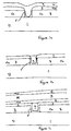
- Figures 1a to 1f are a process flow for the fabrication of a lead in accordance with the present invention.
- FIG. 1a there is shown a typical semiconductor silicon chip 1 to which electrical connection is to be made, such as to a pad thereon or the like.
- An oxide layer 3 is disposed over at least a portion of the surface of the silicon chip 1 and contains a via 5 therethrough extending down to the silicon chip to where the electrical connection is to be made.
- a layer of titanium nitride 7 is deposited in the via 5 as well as over the surface of the oxide layer 3 by sputtering.
- a layer of tungsten 9 is then conformally deposited to fill the via 5 and extend over the titanium nitride layer 7 by chemical vapor deposition.
- the tungsten layer 9 is etched back so that it is now present only within the via 5,
- a layer of titanium nitride 11 is then deposited over the exposed surface followed by a layer of aluminum or aluminum alloy 13, preferably aluminum having 0.5 per cent copper which is then followed by a layer of titanium nitride 15 as shown in Figure 1c.
- the structure of Figure 1c is then masked over the via 5 and slightly beyond the via and isotropic etching then takes place down to the oxide layer 3 as shown in Figure 1d, removing all of the titanium nitride layers 7 and 11, the aluminum layer 13 and the titanium nitride layer 15 except. the portion thereof under the mask (not shown).
- the aluminum layer 15 is etched farther in than are the titanium nitride layers 7, 11 and 15 because the etch chemistry reacts faster toward the aluminum than it does to the titanium nitride.
- Figure 1d The structure of Figure 1d is fully encapsulated by a blanket deposition of a conformal CVD film of titanium nitride 17 as shown in Figure le which is then followed by an isotropic etch of the titanium nitride layer 17, leaving titanium nitride 17 as a sidewall on the aluminum layer 13 as shown in Figure 1f.
Landscapes
- Internal Circuitry In Semiconductor Integrated Circuit Devices (AREA)
- Chemical Vapour Deposition (AREA)
Applications Claiming Priority (2)
| Application Number | Priority Date | Filing Date | Title |
|---|---|---|---|
| US3336196P | 1996-12-18 | 1996-12-18 | |
| US33361P | 1996-12-18 |
Publications (2)
| Publication Number | Publication Date |
|---|---|
| EP0851481A2 true EP0851481A2 (fr) | 1998-07-01 |
| EP0851481A3 EP0851481A3 (fr) | 1999-02-24 |
Family
ID=21869978
Family Applications (1)
| Application Number | Title | Priority Date | Filing Date |
|---|---|---|---|
| EP97204012A Withdrawn EP0851481A3 (fr) | 1996-12-18 | 1997-12-18 | Procédé de fabrication d'un conducteur métallique encapsulé pour interconnexion multi-couche |
Country Status (4)
| Country | Link |
|---|---|
| EP (1) | EP0851481A3 (fr) |
| JP (1) | JP3933776B2 (fr) |
| KR (1) | KR19980064250A (fr) |
| TW (1) | TW386296B (fr) |
Cited By (1)
| Publication number | Priority date | Publication date | Assignee | Title |
|---|---|---|---|---|
| CN113035773A (zh) * | 2019-12-25 | 2021-06-25 | 珠海格力电器股份有限公司 | 芯片封装方法、刻蚀设备及芯片 |
Family Cites Families (4)
| Publication number | Priority date | Publication date | Assignee | Title |
|---|---|---|---|---|
| US4980752A (en) * | 1986-12-29 | 1990-12-25 | Inmos Corporation | Transition metal clad interconnect for integrated circuits |
| FR2667724B1 (fr) * | 1990-10-09 | 1992-11-27 | Thomson Csf | Procede de realisation des metallisations d'electrodes d'un transistor. |
| KR920017186A (ko) * | 1991-02-28 | 1992-09-26 | 원본미기재 | 집적 회로의 도전성 구조 |
| US5757077A (en) * | 1995-02-03 | 1998-05-26 | National Semiconductor Corporation | Integrated circuits with borderless vias |
-
1997
- 1997-12-17 KR KR1019970069927A patent/KR19980064250A/ko not_active Withdrawn
- 1997-12-18 JP JP34971197A patent/JP3933776B2/ja not_active Expired - Fee Related
- 1997-12-18 EP EP97204012A patent/EP0851481A3/fr not_active Withdrawn
-
1998
- 1998-03-13 TW TW086119139A patent/TW386296B/zh not_active IP Right Cessation
Cited By (1)
| Publication number | Priority date | Publication date | Assignee | Title |
|---|---|---|---|---|
| CN113035773A (zh) * | 2019-12-25 | 2021-06-25 | 珠海格力电器股份有限公司 | 芯片封装方法、刻蚀设备及芯片 |
Also Published As
| Publication number | Publication date |
|---|---|
| JP3933776B2 (ja) | 2007-06-20 |
| EP0851481A3 (fr) | 1999-02-24 |
| JPH10189735A (ja) | 1998-07-21 |
| TW386296B (en) | 2000-04-01 |
| KR19980064250A (ko) | 1998-10-07 |
Similar Documents
| Publication | Publication Date | Title |
|---|---|---|
| US5703408A (en) | Bonding pad structure and method thereof | |
| US8749059B2 (en) | Semiconductor device having a copper plug | |
| EP1022776B1 (fr) | Liaison de fil sur cuivre | |
| JP3329380B2 (ja) | 半導体装置およびその製造方法 | |
| US8163629B2 (en) | Metallization for chip scale packages in wafer level packaging | |
| EP1102315A3 (fr) | Méthode pour éviter une contamination par le cuivre des parois d'un trou de contact ou d'une structure à double damasquinage | |
| US6955979B2 (en) | Methods for making metallization structures for semiconductor device interconnects | |
| JP2002500440A (ja) | ウエハ・パッシベーション構造および製造方法 | |
| CN105826246B (zh) | 用于铜结构化的中间层及其形成方法 | |
| US5559056A (en) | Method and apparatus for capping metallization layer | |
| JP2012054588A (ja) | 銅技術相互接続構造を使用する集積回路デバイス用のアルミニウム・パッド電力バスおよび信号ルーティング技術 | |
| US5693564A (en) | Conductor fill reflow with intermetallic compound wetting layer for semiconductor fabrication | |
| JPH11330231A (ja) | 金属被覆構造 | |
| US20090250821A1 (en) | Corrosion resistant via connections in semiconductor substrates and methods of making same | |
| US20020111022A1 (en) | Method of forming embedded copper interconnections and embedded copper interconnection structure | |
| US6175154B1 (en) | Fully encapsulated metal leads for multi-level metallization | |
| US6677647B1 (en) | Electromigration characteristics of patterned metal features in semiconductor devices | |
| US10535576B2 (en) | Semiconductor devices and methods of formation thereof | |
| JP2001313372A (ja) | キャパシタ構造およびその製造方法 | |
| EP0851481A2 (fr) | Procédé de fabrication d'un conducteur métallique encapsulé pour interconnexion multi-couche | |
| US20020068385A1 (en) | Method for forming anchored bond pads in semiconductor devices and devices formed | |
| US6395629B1 (en) | Interconnect method and structure for semiconductor devices | |
| US6417568B1 (en) | Semiconductor device | |
| US5970377A (en) | Method of forming a metal interconnection line for semiconductor device | |
| US20050064705A1 (en) | Method for producing thin metal-containing layers having a low electrical resistance |
Legal Events
| Date | Code | Title | Description |
|---|---|---|---|
| PUAI | Public reference made under article 153(3) epc to a published international application that has entered the european phase |
Free format text: ORIGINAL CODE: 0009012 |
|
| AK | Designated contracting states |
Kind code of ref document: A2 Designated state(s): DE FR GB IT NL |
|
| AX | Request for extension of the european patent |
Free format text: AL;LT;LV;MK;RO;SI |
|
| PUAL | Search report despatched |
Free format text: ORIGINAL CODE: 0009013 |
|
| AK | Designated contracting states |
Kind code of ref document: A3 Designated state(s): AT BE CH DE DK ES FI FR GB GR IE IT LI LU MC NL PT SE |
|
| AX | Request for extension of the european patent |
Free format text: AL;LT;LV;MK;RO;SI |
|
| 17P | Request for examination filed |
Effective date: 19990824 |
|
| AKX | Designation fees paid |
Free format text: DE FR GB IT NL |
|
| 17Q | First examination report despatched |
Effective date: 20080116 |
|
| STAA | Information on the status of an ep patent application or granted ep patent |
Free format text: STATUS: THE APPLICATION HAS BEEN WITHDRAWN |
|
| 18W | Application withdrawn |
Effective date: 20100614 |