EP0851498A2 - Kontaktfläche für Strahlungs-Bildaufnahmevorrichtungen - Google Patents
Kontaktfläche für Strahlungs-Bildaufnahmevorrichtungen Download PDFInfo
- Publication number
- EP0851498A2 EP0851498A2 EP97308467A EP97308467A EP0851498A2 EP 0851498 A2 EP0851498 A2 EP 0851498A2 EP 97308467 A EP97308467 A EP 97308467A EP 97308467 A EP97308467 A EP 97308467A EP 0851498 A2 EP0851498 A2 EP 0851498A2
- Authority
- EP
- European Patent Office
- Prior art keywords
- contact pad
- contact
- array
- photodiode
- radiation imager
- Prior art date
- Legal status (The legal status is an assumption and is not a legal conclusion. Google has not performed a legal analysis and makes no representation as to the accuracy of the status listed.)
- Granted
Links
- 230000005855 radiation Effects 0.000 title claims abstract description 20
- 229910052751 metal Inorganic materials 0.000 claims abstract description 36
- 239000002184 metal Substances 0.000 claims abstract description 36
- 239000000463 material Substances 0.000 claims abstract description 29
- 230000004888 barrier function Effects 0.000 claims abstract description 9
- AMGQUBHHOARCQH-UHFFFAOYSA-N indium;oxotin Chemical compound [In].[Sn]=O AMGQUBHHOARCQH-UHFFFAOYSA-N 0.000 claims abstract description 3
- 239000003989 dielectric material Substances 0.000 claims abstract 2
- 150000002739 metals Chemical class 0.000 claims description 6
- 229910021417 amorphous silicon Inorganic materials 0.000 claims description 4
- 229910052804 chromium Inorganic materials 0.000 claims description 4
- 239000007772 electrode material Substances 0.000 claims description 4
- 229910052750 molybdenum Inorganic materials 0.000 claims description 4
- 229910004205 SiNX Inorganic materials 0.000 claims description 2
- 238000004519 manufacturing process Methods 0.000 abstract description 9
- 238000000034 method Methods 0.000 description 16
- 239000000758 substrate Substances 0.000 description 8
- 230000007797 corrosion Effects 0.000 description 7
- 238000005260 corrosion Methods 0.000 description 7
- 230000015572 biosynthetic process Effects 0.000 description 4
- 238000000151 deposition Methods 0.000 description 4
- 238000000059 patterning Methods 0.000 description 4
- 230000002829 reductive effect Effects 0.000 description 4
- 239000004020 conductor Substances 0.000 description 3
- 238000000623 plasma-assisted chemical vapour deposition Methods 0.000 description 3
- 239000010409 thin film Substances 0.000 description 3
- 230000008021 deposition Effects 0.000 description 2
- 238000003384 imaging method Methods 0.000 description 2
- 238000012986 modification Methods 0.000 description 2
- 230000004048 modification Effects 0.000 description 2
- 229910052581 Si3N4 Inorganic materials 0.000 description 1
- VYPSYNLAJGMNEJ-UHFFFAOYSA-N Silicium dioxide Chemical compound O=[Si]=O VYPSYNLAJGMNEJ-UHFFFAOYSA-N 0.000 description 1
- 229910052782 aluminium Inorganic materials 0.000 description 1
- 230000007547 defect Effects 0.000 description 1
- 230000000593 degrading effect Effects 0.000 description 1
- -1 e.g. Substances 0.000 description 1
- 230000000694 effects Effects 0.000 description 1
- 238000005530 etching Methods 0.000 description 1
- 239000011521 glass Substances 0.000 description 1
- 230000000873 masking effect Effects 0.000 description 1
- 239000011159 matrix material Substances 0.000 description 1
- 238000001465 metallisation Methods 0.000 description 1
- 230000001681 protective effect Effects 0.000 description 1
- 230000002441 reversible effect Effects 0.000 description 1
- HQVNEWCFYHHQES-UHFFFAOYSA-N silicon nitride Chemical compound N12[Si]34N5[Si]62N3[Si]51N64 HQVNEWCFYHHQES-UHFFFAOYSA-N 0.000 description 1
- 229910052814 silicon oxide Inorganic materials 0.000 description 1
- 230000003068 static effect Effects 0.000 description 1
- 239000000126 substance Substances 0.000 description 1
- 238000000427 thin-film deposition Methods 0.000 description 1
- 229910052719 titanium Inorganic materials 0.000 description 1
Images


Classifications
-
- H—ELECTRICITY
- H10—SEMICONDUCTOR DEVICES; ELECTRIC SOLID-STATE DEVICES NOT OTHERWISE PROVIDED FOR
- H10F—INORGANIC SEMICONDUCTOR DEVICES SENSITIVE TO INFRARED RADIATION, LIGHT, ELECTROMAGNETIC RADIATION OF SHORTER WAVELENGTH OR CORPUSCULAR RADIATION
- H10F39/00—Integrated devices, or assemblies of multiple devices, comprising at least one element covered by group H10F30/00, e.g. radiation detectors comprising photodiode arrays
- H10F39/80—Constructional details of image sensors
-
- H—ELECTRICITY
- H10—SEMICONDUCTOR DEVICES; ELECTRIC SOLID-STATE DEVICES NOT OTHERWISE PROVIDED FOR
- H10F—INORGANIC SEMICONDUCTOR DEVICES SENSITIVE TO INFRARED RADIATION, LIGHT, ELECTROMAGNETIC RADIATION OF SHORTER WAVELENGTH OR CORPUSCULAR RADIATION
- H10F77/00—Constructional details of devices covered by this subclass
- H10F77/20—Electrodes
- H10F77/206—Electrodes for devices having potential barriers
-
- H—ELECTRICITY
- H10—SEMICONDUCTOR DEVICES; ELECTRIC SOLID-STATE DEVICES NOT OTHERWISE PROVIDED FOR
- H10F—INORGANIC SEMICONDUCTOR DEVICES SENSITIVE TO INFRARED RADIATION, LIGHT, ELECTROMAGNETIC RADIATION OF SHORTER WAVELENGTH OR CORPUSCULAR RADIATION
- H10F77/00—Constructional details of devices covered by this subclass
- H10F77/93—Interconnections
- H10F77/933—Interconnections for devices having potential barriers
- H10F77/935—Interconnections for devices having potential barriers for photovoltaic devices or modules
-
- Y—GENERAL TAGGING OF NEW TECHNOLOGICAL DEVELOPMENTS; GENERAL TAGGING OF CROSS-SECTIONAL TECHNOLOGIES SPANNING OVER SEVERAL SECTIONS OF THE IPC; TECHNICAL SUBJECTS COVERED BY FORMER USPC CROSS-REFERENCE ART COLLECTIONS [XRACs] AND DIGESTS
- Y02—TECHNOLOGIES OR APPLICATIONS FOR MITIGATION OR ADAPTATION AGAINST CLIMATE CHANGE
- Y02E—REDUCTION OF GREENHOUSE GAS [GHG] EMISSIONS, RELATED TO ENERGY GENERATION, TRANSMISSION OR DISTRIBUTION
- Y02E10/00—Energy generation through renewable energy sources
- Y02E10/50—Photovoltaic [PV] energy
Definitions
- This invention relates generally to contact pads for radiation imagers formed from an array of photosensitive elements, and more particularly to a contact pad structure which is consistent with a process using a reduced number of process steps.
- Radiation imagers with a photosensor array are commonly used in imaging applications such as X-ray imaging and facsimile devices.
- the photosensitive elements in the array typically photodiodes, convert incident radiant energy into a charge which is separated inside the photodiodes by maintaining a reverse bias across all the photodiodes with a common electrode maintained at a predetermined voltage.
- the pixels are disposed in a matrix arrangement with rows and columns of address lines being disposed to enable selective addressing and readout of pixels.
- Each array pixel typically has a photodiode which is connected to a source (or drain) contact of a thin film transistor (TFT).
- TFT thin film transistor
- the address lines oriented along the rows, called scan lines, are typically formed from the same gate metal used for the TFTs.
- the stored photodiode charge on the photodiodes in that row passes onto data lines which are disposed in columns perpendicular to the rows.
- the data lines typically comprise the same material as the source/drain contact material of the TFT.
- Imagers are typically fabricated on large area substrates, such as glass. By a sequence of process steps including thin film deposition, photolithographic patterning and thin film etching, the imager structure is formed on the substrate. Both photodiodes and TFTs preferably comprise amorphous Si (a-Si) deposited, for example, by plasma enhanced chemical vapor deposition (PECVD).
- PECVD plasma enhanced chemical vapor deposition
- Contact fingers are also formed on the substrate during the formation of the array. These contact fingers are extensions of the scan and data lines and common electrode lines from the array to near the perimeter of the substrate and allow connection of external circuitry to the array. At the end of a contact finger is a contact pad, which necessarily has a conducting material as the topmost material over at least part of its surface. Because the number of scan and data address lines on the array may number in the thousands, external contact from driving and read out circuitry is typically made by flexible connectors which are pressed or bonded into contact with the contact pad's surface.
- Structures and methods for fabricating imagers with a reduced number of process steps include United States Patents 5,399,844; 5,435,608 and 5,480,810 issued March 21, 1995; July 25, 1995 and January 2, 1996, respectively, and assigned to the same assignee as the present invention.
- the number of conducting metal depositions is desirably reduced, for example to that of depositing the gate metal and depositing the source/drain (SD) metal; the common electrode can be formed during the same photolithographic patterning step, and from the same material as the source/drain metal, and not from a separate conductor.
- the contact pad is particularly vulnerable to the corrosive effects of moisture because it cannot readily be sealed against moisture exposure due to the necessity of its being in contact with the flexible connectors. Other areas of the photosensor array can be reasonably protected by an inorganic dielectric barrier layer. It has been determined that the metals typically used as the gate and source/drain metals, e.g., Cr, Ti, Mo, and Al, tend to form surface oxides which will inhibit good contact, or are, to varying degrees, susceptible to corrosion.
- the preferred contact pad surface material is indium tin oxide (ITO) or related conducting oxide material as it is less susceptible to these problems.
- ITO has proven to be an insufficient barrier to corrosion of the metal directly underlying it. Moisture can diffuse through the relatively thin polycrystalline ITO and react with underlying metals.
- the source/drain metal or the gate metal are possible choices for the contact pad surface material, which will not require a separate conducting material, they suffer from possible corrosion or contact problems, degrading imager performance and life.
- This invention also seeks to provide a radiation imager contact pad which results in a reduced number of photomasking steps.
- a contact pad for a radiation imager including an array of photodiodes which are fabricated of photodiode material and a conductive oxide, the contact pad comprising:
- a simplified radiation imager contact pad structure may be fabricated simultaneously with the remainder of the radiation imager array so that no process steps beyond those used to fabricate the array are required.
- a contact pad body of the photodiode material may be formed in the contact pad region simultaneously with the formation of the array photodiodes.
- the photodiode may have a layer of ITO on top of it which is the topmost surface to which external electrical contact is made.
- the source and drain electrode material may be patterned to partially overlap the top surface of the photodiode material and to electrically contact, and form part of, the contact fingers.
- An inorganic dielectric barrier may be patterned so that no source and drain electrode material is exposed to ambient conditions, while also leaving ITO exposed on top of the contact pad. Both the scan and data line contact pads may be made in the fashion so as to reduce structural and process complexity.
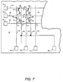
- radiation imager 1 includes a photosensor array 2 on insulating imager substrate 8 including pixels such as 3 (Fig. 7) between the intersections of horizontal scan lines 9 and orthogonal vertical data lines 7.
- Each pixel 3 includes a radiation sensitive element such as photodiode 31 and a thin film transistor (TFT) 32 switch.
- the radiation sensitive element (or photosensor) 31 in each pixel of the array accumulates a charge in response to incident photons.
- Each respective photodiode in a row is addressed by biasing scan lines 9 couple to the gate of respective TFTs in a row so as to selectively cause each TFT to become conductive to enable charge accumulated on the photodiode to be selectively read from output data lines 7 that are coupled to the source (or alternatively the drain) electrode of respective TFTs in a column.
- the bias gating voltages are applied from an external source (not shown) through contact pads such as 15 which are positioned along the outer edges of photosensor array 2.
- Imager 1 may further comprise a ground ring 17 disposed around photosensor array 2 to provide static charge protection. Contact fingers 15 are typically disposed on substrate 8 inside of ground ring 17.
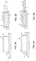
- gate metal 10 of contact pad 15 at the contact pad end of contact fingers 19 is formed on substrate 8 and photodiode body 22 is formed over gate metal 10, which gate metal was previously patterned in the array and contact pad regions.
- the gate metal 10 is not required to underlie the photodiode material 22 in contact pad 15, but it may improve adhesion of the photodiode material 22 relative to its deposition directly onto substrate 8.
- the photodiode material 22 is then patterned and etched to form a plurality of photodiode bodies.
- photodiode material 22 is also patterned into islands in the contact pad 15 region (see FIG. 3). This material is not used as a photosensitive element but becomes part of the pad structure of the contact finger.
- the photodiode material 22 of contact pad 15 consists of layers of doped and undoped a-Si with total thickness of approximately 0.5 to 2.0 microns, and a top layer of ITO 18 with a thickness of approximately 0.1 microns with a range of approximately 0.05 to 0.2 microns.
- the purpose of the thin ITO layer is to enhance the electrical conductivity of top diode layer to improve performance and ensure reliable contact of common electrode 34 to photodiode 31 tops.
- MO 18 forms the top contact surface of the contact pad.
- ITO is a desirable material because it is chemically stable and resists corrosion and the formation of insulating oxides. ITO layer 18 may be substantially coincident with the photodiode material 22 or slightly smaller, depending on the details of the patterning and etch processes.
- a dielectric layer is disposed during dielectric formation of the TFTs 32 in the array.
- Dielectric layer 24 is patterned and etched from the top of the contact pad region 25 as shown in FIG 4, and may be a combination of PECVD silicon nitride (SiNx) and silicon oxide with total thickness of approximately 0.15 to 0.5 microns.
- source and drain metal 26 (Figs. 5 A and 5B) is deposited, patterned and etched to provide electrical contact between ITO layer 18 and the underlying gate metal 10 or the source and drain (SD) metal contact in contact finger 19, thus allowing a continuous contact between the ITO and scan lines 9 and data lines 7 (see FIG. 1).
- SD metal 26 is etched so as to leave ITO 18 exposed over at least a portion of contact pad 15.
- SD metal 26 may comprise, for example, Mo or Cr, or a combination thereof with thickness of approximately 0.1 to 1.0 microns. It is to be noted that the figures are not to scale, particularly in the vertical direction, since the layers are about 2 microns in height, while the exposed ITO contact area is about 150 microns by 2 to 3 mm.
- photosensor array 2 contact fingers 19, and contact pads 1 and 15 are covered with a protective dielectric barrier layer 28 which is patterned and etched so that it is removed from most of the contact pad 15, as shown in FIG. 6A and 6B.
- Barrier layer 28 entirely covers the SD metal 26, including the region where SD metal 26 contacts ITO layer 18. This inhibits chemical corrosion and damage to SD metal 26 and ITO layer 18.
- the common electrical contact of diodes 31 is fabricated from the same layer (and material) used to form the source and drain electrodes of TFTs 32 and data lines 7.
- the common electrode lines are positioned halfway between adjacent data lines, effectively making a common electrode 34 (see FIG. 7) out of SD electrode material 26 with the vertical lines connected at the edges of radiation imager 1, and by using diode islands 22 in contact pad 15.
- One or more contact pads 35 are provided to enable external connection to common electrode 34.
- SD metal 26 and common electrode layer 34 each comprise, for example, Mo or Cr; other metals, or multi-layers of metals may be used, but Al presents challenges because during a wet etch (e.g., see FIGS. 5A and 5B) corrosion of exposed ITO layer 18 may occur. If Al is required as the SD metal 26 for electric noise purposes, an additional metal layer (not shown) which connects contact fingers 19 to ITO 18 on top of contact pad 15 is typically deposited.
- Putting the diode island material in the contact pad structures enables use of the ITO layers 18 on the diode island material for contact, thus eliminating the need for an additional contact layer and its associated masking step.
- SD metal 26 used for the source and drain electrodes of transistors 32 is also used for data lines 7 and common electrode lines 34, all of which are formed at the same time by the same process steps.
- the gate electrode metal of transistors 32 and scan lines 9 are formed of the same metal and at the same time and by the same process steps.
- the cross section of fingers 19 may not be identical to the cross section of the array 2 lines to which they are electrically connected, and the fingers may vary in cross section from one another.
- the subject invention utilizing a combination SD metal and common electrode layer reduces the number of photomask process steps required for the fabrication of the contact pad, reducing fabrication time, expense, and possible problems or defects introduced by an additional process step if it were required.
- the process requires only three conductive layer depositions (and associated photomask and etch steps) which are disposed in the following order: gate metal 10, ITO strap 18 on photodiode material 22, and the SD metal 26 which also forms common electrode lines which run across and connect the tops of the photodiodes.
Landscapes
- Solid State Image Pick-Up Elements (AREA)
- Light Receiving Elements (AREA)
- Transforming Light Signals Into Electric Signals (AREA)
- Photovoltaic Devices (AREA)
Applications Claiming Priority (2)
| Application Number | Priority Date | Filing Date | Title |
|---|---|---|---|
| US772453 | 1996-12-23 | ||
| US08/772,453 US5838054A (en) | 1996-12-23 | 1996-12-23 | Contact pads for radiation imagers |
Publications (3)
| Publication Number | Publication Date |
|---|---|
| EP0851498A2 true EP0851498A2 (de) | 1998-07-01 |
| EP0851498A3 EP0851498A3 (de) | 1999-04-21 |
| EP0851498B1 EP0851498B1 (de) | 2007-03-07 |
Family
ID=25095118
Family Applications (1)
| Application Number | Title | Priority Date | Filing Date |
|---|---|---|---|
| EP97308467A Expired - Lifetime EP0851498B1 (de) | 1996-12-23 | 1997-10-23 | Kontaktfläche für Strahlungs-Bildaufnahmevorrichtungen |
Country Status (4)
| Country | Link |
|---|---|
| US (1) | US5838054A (de) |
| EP (1) | EP0851498B1 (de) |
| JP (1) | JP3964017B2 (de) |
| DE (1) | DE69737439T2 (de) |
Cited By (1)
| Publication number | Priority date | Publication date | Assignee | Title |
|---|---|---|---|---|
| EP1052697A3 (de) * | 1999-05-11 | 2004-03-24 | Yokogawa Electric Corporation | Photodiodenanordnung |
Families Citing this family (11)
| Publication number | Priority date | Publication date | Assignee | Title |
|---|---|---|---|---|
| DE19820816B4 (de) * | 1998-05-09 | 2006-05-11 | Robert Bosch Gmbh | Bondpadstruktur und entsprechendes Herstellungsverfahren |
| JP3869952B2 (ja) * | 1998-09-21 | 2007-01-17 | キヤノン株式会社 | 光電変換装置とそれを用いたx線撮像装置 |
| US6373117B1 (en) * | 1999-05-03 | 2002-04-16 | Agilent Technologies, Inc. | Stacked multiple photosensor structure including independent electrical connections to each photosensor |
| US6396046B1 (en) * | 1999-11-02 | 2002-05-28 | General Electric Company | Imager with reduced FET photoresponse and high integrity contact via |
| US6777685B2 (en) * | 2002-04-03 | 2004-08-17 | General Electric Company | Imaging array and methods for fabricating same |
| US6559506B1 (en) | 2002-04-03 | 2003-05-06 | General Electric Company | Imaging array and methods for fabricating same |
| US6740884B2 (en) * | 2002-04-03 | 2004-05-25 | General Electric Company | Imaging array and methods for fabricating same |
| US6784434B2 (en) * | 2002-06-25 | 2004-08-31 | General Electric Company | Imaging array and method for manufacturing same |
| US7307301B2 (en) * | 2002-12-17 | 2007-12-11 | General Electric Company | Imaging array |
| KR100649034B1 (ko) * | 2005-09-21 | 2006-11-27 | 동부일렉트로닉스 주식회사 | 씨모스 이미지 센서의 제조방법 |
| WO2016104339A1 (ja) * | 2014-12-25 | 2016-06-30 | シャープ株式会社 | フォトセンサ基板、及びその製造方法 |
Family Cites Families (9)
| Publication number | Priority date | Publication date | Assignee | Title |
|---|---|---|---|---|
| US4012767A (en) * | 1976-02-25 | 1977-03-15 | General Electric Company | Electrical interconnections for semi-conductor devices |
| JPS62128571A (ja) * | 1985-11-29 | 1987-06-10 | Fuji Electric Co Ltd | アモルフアスシリコン太陽電池 |
| US4725890A (en) * | 1986-07-15 | 1988-02-16 | Ovonic Imaging Systems, Inc. | Flexible array of photosensitive elements |
| US4739414A (en) * | 1986-07-15 | 1988-04-19 | Ovonic Imaging Systems, Inc. | Large area array of thin film photosensitive elements for image detection |
| US4889983A (en) * | 1987-11-24 | 1989-12-26 | Mitsubishi Denki Kabushiki Kaisha | Image sensor and production method thereof |
| JPH0423470A (ja) * | 1990-05-18 | 1992-01-27 | Fuji Xerox Co Ltd | イメージセンサ |
| EP0517208A1 (de) * | 1991-06-05 | 1992-12-09 | Kanegafuchi Kagaku Kogyo Kabushiki Kaisha | Halbleitervorrichtung und deren Herstellungsprozess |
| US5532180A (en) * | 1995-06-02 | 1996-07-02 | Ois Optical Imaging Systems, Inc. | Method of fabricating a TFT with reduced channel length |
| US5614727A (en) * | 1995-06-06 | 1997-03-25 | International Business Machines Corporation | Thin film diode having large current capability with low turn-on voltages for integrated devices |
-
1996
- 1996-12-23 US US08/772,453 patent/US5838054A/en not_active Expired - Lifetime
-
1997
- 1997-10-21 JP JP28750197A patent/JP3964017B2/ja not_active Expired - Fee Related
- 1997-10-23 DE DE69737439T patent/DE69737439T2/de not_active Expired - Lifetime
- 1997-10-23 EP EP97308467A patent/EP0851498B1/de not_active Expired - Lifetime
Cited By (2)
| Publication number | Priority date | Publication date | Assignee | Title |
|---|---|---|---|---|
| EP1052697A3 (de) * | 1999-05-11 | 2004-03-24 | Yokogawa Electric Corporation | Photodiodenanordnung |
| EP2249388A3 (de) * | 1999-05-11 | 2012-08-22 | Yokogawa Electric Corporation | Photodiodenanordnung |
Also Published As
| Publication number | Publication date |
|---|---|
| JPH10214955A (ja) | 1998-08-11 |
| EP0851498A3 (de) | 1999-04-21 |
| US5838054A (en) | 1998-11-17 |
| EP0851498B1 (de) | 2007-03-07 |
| DE69737439T2 (de) | 2007-11-08 |
| JP3964017B2 (ja) | 2007-08-22 |
| DE69737439D1 (de) | 2007-04-19 |
Similar Documents
| Publication | Publication Date | Title |
|---|---|---|
| US6465861B1 (en) | Corrosion resistant imager | |
| US5480810A (en) | Method of fabricating a radiation imager with common passivation dielectric for gate electrode and photosensor | |
| EP0652596B1 (de) | Bildaufnehmer und Herstellungsverfahren | |
| US6680216B2 (en) | Method of making imager structure | |
| US5233181A (en) | Photosensitive element with two layer passivation coating | |
| US6806472B2 (en) | Switching device of an X-ray sensor and method for manufacturing the same | |
| JP4600964B2 (ja) | ゲーテッドフォトダイオードを有する固体イメージャ及びその製造方法 | |
| EP0851498B1 (de) | Kontaktfläche für Strahlungs-Bildaufnahmevorrichtungen | |
| EP1351310A2 (de) | Bildmarix und deren Verfahren zur Herstellung | |
| US20250318291A1 (en) | Semiconductor device | |
| US5859463A (en) | Photosensitive imager contact pad structure | |
| US7633091B2 (en) | Structure for an image TFT array for an indirect X-ray sensor | |
| US5777355A (en) | Radiation imager with discontinuous dielectric | |
| US7338833B2 (en) | Dual dielectric structure for suppressing lateral leakage current in high fill factor arrays | |
| EP0890190B1 (de) | Korrosionsbeständige bildaufnahmevorrichtung | |
| WO1998032173A9 (en) | Corrosion resistant imager | |
| KR100532025B1 (ko) | 박막트랜지스터 광센서 및 그 제조방법_ | |
| CA2247717A1 (en) | Corrosion resistant imager | |
| JPH0661466A (ja) | 光電変換素子及びその製造方法 |
Legal Events
| Date | Code | Title | Description |
|---|---|---|---|
| PUAI | Public reference made under article 153(3) epc to a published international application that has entered the european phase |
Free format text: ORIGINAL CODE: 0009012 |
|
| AK | Designated contracting states |
Kind code of ref document: A2 Designated state(s): DE FR GB IT |
|
| PUAL | Search report despatched |
Free format text: ORIGINAL CODE: 0009013 |
|
| AK | Designated contracting states |
Kind code of ref document: A3 Designated state(s): AT BE CH DE DK ES FI FR GB GR IE IT LI LU MC NL PT SE |
|
| 17P | Request for examination filed |
Effective date: 19991021 |
|
| AKX | Designation fees paid |
Free format text: DE FR GB IT |
|
| 17Q | First examination report despatched |
Effective date: 20000503 |
|
| GRAP | Despatch of communication of intention to grant a patent |
Free format text: ORIGINAL CODE: EPIDOSNIGR1 |
|
| GRAS | Grant fee paid |
Free format text: ORIGINAL CODE: EPIDOSNIGR3 |
|
| GRAA | (expected) grant |
Free format text: ORIGINAL CODE: 0009210 |
|
| AK | Designated contracting states |
Kind code of ref document: B1 Designated state(s): DE FR GB IT |
|
| REG | Reference to a national code |
Ref country code: GB Ref legal event code: FG4D |
|
| REF | Corresponds to: |
Ref document number: 69737439 Country of ref document: DE Date of ref document: 20070419 Kind code of ref document: P |
|
| ET | Fr: translation filed | ||
| PLBE | No opposition filed within time limit |
Free format text: ORIGINAL CODE: 0009261 |
|
| STAA | Information on the status of an ep patent application or granted ep patent |
Free format text: STATUS: NO OPPOSITION FILED WITHIN TIME LIMIT |
|
| 26N | No opposition filed |
Effective date: 20071210 |
|
| PGFP | Annual fee paid to national office [announced via postgrant information from national office to epo] |
Ref country code: GB Payment date: 20141027 Year of fee payment: 18 Ref country code: FR Payment date: 20141017 Year of fee payment: 18 Ref country code: DE Payment date: 20141029 Year of fee payment: 18 |
|
| PGFP | Annual fee paid to national office [announced via postgrant information from national office to epo] |
Ref country code: IT Payment date: 20141028 Year of fee payment: 18 |
|
| REG | Reference to a national code |
Ref country code: DE Ref legal event code: R119 Ref document number: 69737439 Country of ref document: DE |
|
| GBPC | Gb: european patent ceased through non-payment of renewal fee |
Effective date: 20151023 |
|
| PG25 | Lapsed in a contracting state [announced via postgrant information from national office to epo] |
Ref country code: GB Free format text: LAPSE BECAUSE OF NON-PAYMENT OF DUE FEES Effective date: 20151023 Ref country code: DE Free format text: LAPSE BECAUSE OF NON-PAYMENT OF DUE FEES Effective date: 20160503 Ref country code: IT Free format text: LAPSE BECAUSE OF NON-PAYMENT OF DUE FEES Effective date: 20151023 |
|
| REG | Reference to a national code |
Ref country code: FR Ref legal event code: ST Effective date: 20160630 |
|
| PG25 | Lapsed in a contracting state [announced via postgrant information from national office to epo] |
Ref country code: FR Free format text: LAPSE BECAUSE OF NON-PAYMENT OF DUE FEES Effective date: 20151102 |