EP0851625A2 - Dispositif de synchronisation de l'horloge d'un récepteur utilisant l'horloge des données à phases - Google Patents
Dispositif de synchronisation de l'horloge d'un récepteur utilisant l'horloge des données à phasesInfo
- Publication number
- EP0851625A2 EP0851625A2 EP97122539A EP97122539A EP0851625A2 EP 0851625 A2 EP0851625 A2 EP 0851625A2 EP 97122539 A EP97122539 A EP 97122539A EP 97122539 A EP97122539 A EP 97122539A EP 0851625 A2 EP0851625 A2 EP 0851625A2
- Authority
- EP
- European Patent Office
- Prior art keywords
- phase
- clock
- received data
- retiming
- accordance
- Prior art date
- Legal status (The legal status is an assumption and is not a legal conclusion. Google has not performed a legal analysis and makes no representation as to the accuracy of the status listed.)
- Withdrawn
Links
- 230000001360 synchronised effect Effects 0.000 claims abstract description 20
- 238000012935 Averaging Methods 0.000 claims description 18
- 230000010355 oscillation Effects 0.000 abstract description 6
- 238000010586 diagram Methods 0.000 description 9
- 230000000630 rising effect Effects 0.000 description 7
- 238000000034 method Methods 0.000 description 6
- 230000005540 biological transmission Effects 0.000 description 3
- 230000000717 retained effect Effects 0.000 description 3
- 230000006866 deterioration Effects 0.000 description 2
- 239000000470 constituent Substances 0.000 description 1
- 238000009795 derivation Methods 0.000 description 1
- 238000001514 detection method Methods 0.000 description 1
- 230000000694 effects Effects 0.000 description 1
- 230000014509 gene expression Effects 0.000 description 1
- 230000007704 transition Effects 0.000 description 1
Images






Classifications
-
- H—ELECTRICITY
- H04—ELECTRIC COMMUNICATION TECHNIQUE
- H04L—TRANSMISSION OF DIGITAL INFORMATION, e.g. TELEGRAPHIC COMMUNICATION
- H04L7/00—Arrangements for synchronising receiver with transmitter
- H04L7/02—Speed or phase control by the received code signals, the signals containing no special synchronisation information
- H04L7/033—Speed or phase control by the received code signals, the signals containing no special synchronisation information using the transitions of the received signal to control the phase of the synchronising-signal-generating means, e.g. using a phase-locked loop
- H04L7/0337—Selecting between two or more discretely delayed clocks or selecting between two or more discretely delayed received code signals
- H04L7/0338—Selecting between two or more discretely delayed clocks or selecting between two or more discretely delayed received code signals the correction of the phase error being performed by a feed forward loop
-
- H—ELECTRICITY
- H03—ELECTRONIC CIRCUITRY
- H03L—AUTOMATIC CONTROL, STARTING, SYNCHRONISATION OR STABILISATION OF GENERATORS OF ELECTRONIC OSCILLATIONS OR PULSES
- H03L7/00—Automatic control of frequency or phase; Synchronisation
- H03L7/06—Automatic control of frequency or phase; Synchronisation using a reference signal applied to a frequency- or phase-locked loop
- H03L7/08—Details of the phase-locked loop
- H03L7/081—Details of the phase-locked loop provided with an additional controlled phase shifter
- H03L7/0812—Details of the phase-locked loop provided with an additional controlled phase shifter and where no voltage or current controlled oscillator is used
- H03L7/0814—Details of the phase-locked loop provided with an additional controlled phase shifter and where no voltage or current controlled oscillator is used the phase shifting device being digitally controlled
-
- H—ELECTRICITY
- H03—ELECTRONIC CIRCUITRY
- H03L—AUTOMATIC CONTROL, STARTING, SYNCHRONISATION OR STABILISATION OF GENERATORS OF ELECTRONIC OSCILLATIONS OR PULSES
- H03L7/00—Automatic control of frequency or phase; Synchronisation
- H03L7/06—Automatic control of frequency or phase; Synchronisation using a reference signal applied to a frequency- or phase-locked loop
- H03L7/08—Details of the phase-locked loop
- H03L7/081—Details of the phase-locked loop provided with an additional controlled phase shifter
- H03L7/0812—Details of the phase-locked loop provided with an additional controlled phase shifter and where no voltage or current controlled oscillator is used
- H03L7/0816—Details of the phase-locked loop provided with an additional controlled phase shifter and where no voltage or current controlled oscillator is used the controlled phase shifter and the frequency- or phase-detection arrangement being connected to a common input
-
- H—ELECTRICITY
- H03—ELECTRONIC CIRCUITRY
- H03L—AUTOMATIC CONTROL, STARTING, SYNCHRONISATION OR STABILISATION OF GENERATORS OF ELECTRONIC OSCILLATIONS OR PULSES
- H03L7/00—Automatic control of frequency or phase; Synchronisation
- H03L7/06—Automatic control of frequency or phase; Synchronisation using a reference signal applied to a frequency- or phase-locked loop
- H03L7/08—Details of the phase-locked loop
- H03L7/085—Details of the phase-locked loop concerning mainly the frequency- or phase-detection arrangement including the filtering or amplification of its output signal
Definitions
- the present invention relates to a data synchronization circuit and particularly to a data synchronization circuit wherein a phase synchronization is obtained using a clock synchronized with a bit of the relevant received data.
- one of the techniques for extracting and reproducing a transmitted digital signal on the receiving side is a bit synchronization technique.
- it is required to receive a digital signal having a phase variation without errors.
- bit synchronization circuit used in the transmission of digital signals between a plurality of apparatus operating with a clock supplied from one and the same clock source (synchronized in frequency)
- PLL Circuit by Polyphase Clock described in Japanese Patent Laid-Open No. 43919/1987 is known.
- FIG. 14 is a block diagram showing a conventional bit synchronization circuit.
- n-phase clocks 12-1 to 12-n are applied via input clock terminals 2-1 to 2-n to the clock selector 47, which have the same frequency as that of the received data signal and phases different by 360/n (n: integer equal to or greater than 2).
- This clock selector 47 selects the clock corresponding to a count value of the up-down counter 46 from the n-phase clocks and outputs it to the output clock terminal 9 as an extracted clock 48.
- the phase comparison circuit 45 compares the phase of a received data signal 11 inputted via the input data terminal 1 and that of the extracted clock 48.
- the up-down counter 46 performs an increment and decrement in the count value to perform a selective control of the clock selector 47.
- the first problem is a problem that the synchronization operation may not converge to induce oscillations in the conventional bit synchronization circuit, thereby leading to a deterioration in receiving characteristics.
- the synchronization operation may not converge to induce oscillations and the most suitable extracted clock to received data is not selected in cases where the propagation delay time of a phase control signal (time taken for the phase comparison result to propagate to the clock selector) is greater than the time of a period in the phase comparison.
- the second problem is a problem that the phase synchronism between a received data signal and the extracted clock may lose, thereby leading to a deterioration in receiving characteristics.
- the most suitable extracted clock to received data is not selected as follows.
- a received data signal having a short-period phase variation such as zitter is inputted, the phase of the extracted clock also varies corresponding to a phase variation of the received data signal.
- phase variations between the received data signal and the extracted clock have a time lag by the propagation delay time of a phase control signal, the phase synchronism between the received data signal and the extracted clock loses and consequently the most suitable extracted clock to received data is not selected.
- a data synchronization circuit for extracting a clock synchronized with a received data from multi-phase clocks that are equal in frequency to the received data and successively shift in phase so as to subject the received data to retiming in accordance with this extracted clock, comprising phase comparing means for comparing the phase of the received data with that of each of the above multi-phase clocks to generate a specific signal for specifying one of the multi-phase clocks having a predetermined phase relation with the received data, retiming means for retiming the received data in accordance with the extracted clock, averaging means for averaging and outputting the specific signal in synchronism with an output of the retiming means, selective means for selectively extracting the multi-phase clocks in response to this averaged output and means for retiming the received data for derivation in accordance with the clock extracted by the selective means.
- the above averaging means is featured by having retiming means for retiming the averaged output in accordance with the extracted clock to output it to the selective means.
- phase comparing means comprises latch means for latching each of the multi-phase clocks in accordance with the received data and encoding means for encoding these latch outputs in accordance with a predetermined rule to make the specific signal.
- the extracted clock and the extracted data are selectively outputted from the multi-phased clocks and the received data sampled by the muti-phased clocks, respectively, thereby enabling the extracted clock synchronized in phase to be outputted and the extracted data subjected to retiming without errors to be outputted even when received data signal having a phase synchronism such as zittr is inputted.
- FIG. 1 is a block diagram of one embodiment of the present invention. Parts similar to those of FIG. 14 are denoted by like symbols.
- the frequency divider circuit 19 divides the data 11 inputted from the input terminal 1 according to the frequency and outputs them as frequency divided data 20.
- the F/F (flip flop) 3 subjects the received data 11 to retiming in accordance with the extracted clock 17 selectively extracted by the clock selector 7 to lead out the identified data 16 to the output terminal 8.
- the phase comparison circuit 4 compares the phase of the frequency divided data 20 with each phase of the n-phase clocks 12-1 to 12-n (n: integer equal to or greater than 2) and generates a specific signal 14 for specifying one of the n-phase clocks having a predetermined phase relation with the frequency divided data 20.
- the averaging circuit 5 averages the specific signals 14 from the phase comparator circuit 4 in time series to generate averaged signals 15-1 to 15-n patterned.
- the change point synchronizing circuit 6 subjects the frequency divided data 20 to retiming in accordance with the extracted clock 17 and outputs them, by which the change point of the frequency divided data is synchronized in accordance with the extracted clock 17 and is outputted. In synchronism with this change point synchronized signal 13, the average processing of the averaging circuit 5 is so arranged as to be performed.
- the F/F 10-1 to 10-n output each of n-bit averaged signals 15-1 to 15-n after the retiming in accordance with the extracted clock 17 and the clock selector 7 selects one of the n-phase clocks 12-1 to 12-n in response to these retimed averaged signals 18-1 to 18-n and leads out it as the extracted clock 17.
- This extracted clock 17 is not only outputted to the output terminal 9 but also serves as a clock input to F/F 3 for the identification of the received data 11.
- the received data 11 are signals repeating changes between 0 and 1 every time as shown in FIG. 7 and assuming that the frequency dividing radio of the frequency divider circuit 19 is "1/2"
- the frequency divided data 20 are synchronized (retimed) with the rising edge of the extracted clock 17 and a change point synchronized signal 13 is generated.
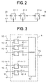
- this change point synchronization detection circuit 6 is a cascade connection circuitry of p ("p" is an integer not greater than the frequency dividing ratio of the frequency dividing circuit 19) constituents F/F 61-1 to 61-p as shown in FIG. 2, where the frequency divided data 20 become a D input to the first step F/F 61-1, the Q output of this F/F 61-1 becomes a D input of the next step F/F 61-2. The further proceeds in a similar way and the Q output of the final step 61-p becomes the change point synchronized signal 13. To the clock (C) inputs of individual F/F is applied the extracted clock 17.
- the frequency divided data 20 and the extracted clock 17 are asynchronous signals and in synchronism with the rising edge of the extracted clock 17 later than that of the frequency divided data 20, the change point synchronized signal 13 is obtained.
- FIG. 3 is a circuit diagram showing one example of phase comparator circuit 4.
- To the D inputs of the F/F 41-1 to 41-n are inputted n-phase clocks 12-1 to 12-n, respectively and to the clock (C) inputs thereof is inputted the received data 11 (when the frequency dividing ratio is 1, generally their frequency divided data 20).
- Q outputs 42-1 to 42-n of individual F/F 41-1 to 41-n are inputted to the encoder 43 and encoded as the closest clock phase information (phase information for specifying one of the n-phase clocks) 14 to the change point phase of the received data 11.
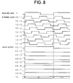
- FIG. 8 is a time chart showing the operation of the phase comparator circuit 4 in FIG. 3.
- By latching the 8-phase clocks 12-1 to 12-8 inputted to the F/F 41-1 to 41-8 (n 8) with the rising edge of the received data 11, output data 42-1 to 42-8 are obtained.
- These latch outputs 42-1 to 42-8 are encoded into a phase comparing signal 14 by the encoder 43.
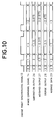
- the encode logic of this encoder 43 is shown in FIG. 9.
- phase comparing signals 14 For values of phase comparing signals 14 outputted from the encoder 43, a one-to-one correspondence is previously established to 8 types of 8-phase clocks 12-1 to 12-8, respectively in terms of 3-bit expressions ("000" to "111"). If the rising edge of the received data 11 lies between the that of an 8-phase clock 12-1 and that of an 8-phase clock 12-2 as shown in FIG. 8, values of the output data 42-1 to 42-8 become "10000111". A value of phase comparison signal 14 at this time is found from FIG. 9 to become "-3" and consequently the 8-phase clock 12-6 is specified.
- FIG. 4 shows the circuitry of one embodiment of averaging circuit 5 shown in FIG. 1.
- the phase comparison signal 14 of the phase comparator circuit 4 is inputted to the minuend signal input of the subtracter 21.
- the storage section 24 inputs the change point synchronized signal 13 as a clock signal and retains the status of addition operation result from the adder 23 to output it to the numerical operation section 25.
- the subtracter 21 outputs the subtracted result obtained by subtracting the output value 28 of the storage section 24 from a phase comparison signal 14 to the 1/m weighting section 22.
- the 1/m weighting section 22 performs a 1/m remainder operation and outputs the remainder operation result to the adder 23.
- the adder 23 performs an addition operation of the remainder result from the 1/m weighting section 22 to an output value 28 of the storage section 24 and outputs the corrected average value to the storage section 24.
- the numerical value operation section 25 rounds an output value 28 of the storage section 24 to an integer and obtains the averages 29-1 to 29-N of phase comparison signals. These average values 29-1 to 29-N are retimed by the F/F 30-1 to 30-n in accordance with the change point synchronized signal 13 and the averaged signals 15-1 to 15-n are outputted.
- FIG. 11 shows the logic of an input signal 28 and the output signals 29-1 to 29-8 of the numerical value operation section 25.
- FIG. 5 shows the circuitry of one embodiment of clock selector 7 shown in FIG. 1.
- Individual retimed signals 18-1 to 18-n of the averaged signals 15-1 to 15-n are inputted to the latch circuits 51-1 to 51-n and outputs 54-1 to 54-n latched with n-phase clock signals 12-1 to 12-n are inputted to one input of 2-input AND circuits 52-1 to 52-n.
- Inputted to the other input of 2-input AND circuits 52-1 to 52-n are n-phase clock signals 12-1 to 12-n and output signals 55-1 to 55-n are inputted to the n-input OR circuit 53.
- the n-input OR circuit 53 outputs an extracted clock signal 17.
- FIGS. 12 and 13 are time charts showing the operation of the clock selector 7 in FIG. 5.
- care should be taken so that no impulse noise appears at the switching time of selection and this circuit satisfies this demand.
- FIG. 12 shows the process transmitting from the state of the clock 12-2 being selected by the selector in FIG. 5 to that of the clock 12-1 being selected.
- the selection signals 18-1 to 18-n take a value of 1 only for 18-2 and a value of 0 for others.
- the new selection signals 18-1 to 18-n are inputted after a lag from the rising edge of the clock 12-2 and they take a value of 1 only for 18-1 and a value of 0 for others.
- the latch circuits 51-1 to 51-n in FIG. 5 are in the sample state for a latch signal of 0 and in the hold state for a latch signal of 1. Thus, the latch outputs 54-1 and 54-2 are retained till the rise of the n-phase clock signals 12-1 and 12-2.
- the outputs 55-1 and 55-2 of the 2-input AND circuits become respectively as shown in FIG. 12 and the extracted clock 17 of output of the n-input OR circuit ends in switching from 12-2 to 12-1 of the n-phase clocks.
- FIG. 13 shows the process of transition from the state of the clock 12-2 being selected by the selector to that of the clock 12-3 being selected. Both in the case of FIG. 12 and in the case of FIG. 13, it is shown that switching takes place without appearance of a impulse noise in the extracted clock 17.
- the second embodiment of the present invention it is also allowable to omit the F/F 10-1 to 10-n in FIG. 1 and employ the averaged signals 15-1 to 15-n directly as the selected signals of the clock selector 7. As faults of this case, it may be mentioned that the clock selector 7 becomes too critical in operation to operate at high speed.
- the third embodiment it is also allowable to omit the frequency divider circuits 19 in FIG. 1 and employ the received data 11 as the frequency divided data 20.
- the averaging circuit 5 or the like becomes too critical in operation to operate at high speed.
Landscapes
- Engineering & Computer Science (AREA)
- Computer Networks & Wireless Communication (AREA)
- Signal Processing (AREA)
- Synchronisation In Digital Transmission Systems (AREA)
- Dc Digital Transmission (AREA)
Applications Claiming Priority (2)
| Application Number | Priority Date | Filing Date | Title |
|---|---|---|---|
| JP344355/96 | 1996-12-25 | ||
| JP08344355A JP3125699B2 (ja) | 1996-12-25 | 1996-12-25 | データ同期回路 |
Publications (1)
| Publication Number | Publication Date |
|---|---|
| EP0851625A2 true EP0851625A2 (fr) | 1998-07-01 |
Family
ID=18368605
Family Applications (1)
| Application Number | Title | Priority Date | Filing Date |
|---|---|---|---|
| EP97122539A Withdrawn EP0851625A2 (fr) | 1996-12-25 | 1997-12-19 | Dispositif de synchronisation de l'horloge d'un récepteur utilisant l'horloge des données à phases |
Country Status (3)
| Country | Link |
|---|---|
| US (1) | US6002731A (fr) |
| EP (1) | EP0851625A2 (fr) |
| JP (1) | JP3125699B2 (fr) |
Cited By (1)
| Publication number | Priority date | Publication date | Assignee | Title |
|---|---|---|---|---|
| EP1376863A3 (fr) * | 2002-05-08 | 2006-01-04 | NEC Electronics Corporation | Méthode et circuit de production d'un signal de contrôle pour l'adaptation d'impédance |
Families Citing this family (13)
| Publication number | Priority date | Publication date | Assignee | Title |
|---|---|---|---|---|
| US6148052A (en) * | 1997-12-10 | 2000-11-14 | Nortel Networks Corporation | Digital phase detector with ring oscillator capture and inverter delay calibration |
| JP3189774B2 (ja) * | 1998-01-28 | 2001-07-16 | 日本電気株式会社 | ビット同期回路 |
| JP3371831B2 (ja) * | 1998-12-07 | 2003-01-27 | 日本電気株式会社 | ビット同期方法及びその装置 |
| JP3376315B2 (ja) * | 1999-05-18 | 2003-02-10 | 日本電気株式会社 | ビット同期回路 |
| US6850580B1 (en) * | 1999-06-21 | 2005-02-01 | Sharp Kabushiki Kaisha | Bit synchronizing circuit |
| JP3573661B2 (ja) | 1999-06-24 | 2004-10-06 | Necエレクトロニクス株式会社 | クロック信号制御方法及び回路とこれを用いたデータ伝送装置 |
| JP2001168848A (ja) * | 1999-12-07 | 2001-06-22 | Mitsubishi Electric Corp | デジタル同期回路 |
| US7194059B2 (en) * | 2001-08-17 | 2007-03-20 | Zarlink Semiconductor, Inc. | Method and apparatus for skip-free retiming transmission of digital information |
| JP4137005B2 (ja) * | 2004-05-25 | 2008-08-20 | Necエレクトロニクス株式会社 | 位相同期回路 |
| US20060187729A1 (en) * | 2005-02-24 | 2006-08-24 | Broadcom Corporation | Source synchronous communication channel interface receive logic |
| US20060188046A1 (en) * | 2005-02-24 | 2006-08-24 | Broadcom Corporation | Prediction of an optimal sampling point for clock resynchronization in a source synchronous data channel |
| JP2007189293A (ja) * | 2006-01-11 | 2007-07-26 | Matsushita Electric Ind Co Ltd | クロック発生回路 |
| US7974036B2 (en) * | 2008-08-19 | 2011-07-05 | Seagate Technology Llc | Time-shifted bits for write synchronization correction |
Family Cites Families (12)
| Publication number | Priority date | Publication date | Assignee | Title |
|---|---|---|---|---|
| JPS61127243A (ja) * | 1984-11-26 | 1986-06-14 | Hitachi Ltd | ビツト位相同期回路 |
| JPS6243919A (ja) * | 1985-08-22 | 1987-02-25 | Meidensha Electric Mfg Co Ltd | 多相クロック発生用pll回路 |
| US4996444A (en) * | 1989-09-21 | 1991-02-26 | Northern Telecom Limited | Clock recovery circuit |
| US5138633A (en) * | 1990-11-19 | 1992-08-11 | At&T Bell Laboratories | Method and apparatus for adaptively retiming and regenerating digital pulse signals |
| JPH04319829A (ja) * | 1991-04-19 | 1992-11-10 | Fujitsu Ltd | 位相同期回路 |
| US5341405A (en) * | 1991-06-11 | 1994-08-23 | Digital Equipment Corporation | Data recovery apparatus and methods |
| JPH0591096A (ja) * | 1991-06-26 | 1993-04-09 | Clarion Co Ltd | クロツク再生回路 |
| US5757857A (en) * | 1994-07-21 | 1998-05-26 | The Regents Of The University Of California | High speed self-adjusting clock recovery circuit with frequency detection |
| JP2773669B2 (ja) * | 1995-03-01 | 1998-07-09 | 日本電気株式会社 | ディジタルpll回路 |
| US5608357A (en) * | 1995-09-12 | 1997-03-04 | Vlsi Technology, Inc. | High speed phase aligner with jitter removal |
| US5712580A (en) * | 1996-02-14 | 1998-01-27 | International Business Machines Corporation | Linear phase detector for half-speed quadrature clocking architecture |
| JP2806863B2 (ja) * | 1996-02-27 | 1998-09-30 | 日本電気エンジニアリング株式会社 | ビット同期回路 |
-
1996
- 1996-12-25 JP JP08344355A patent/JP3125699B2/ja not_active Expired - Fee Related
-
1997
- 1997-12-19 EP EP97122539A patent/EP0851625A2/fr not_active Withdrawn
- 1997-12-22 US US08/995,345 patent/US6002731A/en not_active Expired - Fee Related
Cited By (1)
| Publication number | Priority date | Publication date | Assignee | Title |
|---|---|---|---|---|
| EP1376863A3 (fr) * | 2002-05-08 | 2006-01-04 | NEC Electronics Corporation | Méthode et circuit de production d'un signal de contrôle pour l'adaptation d'impédance |
Also Published As
| Publication number | Publication date |
|---|---|
| US6002731A (en) | 1999-12-14 |
| JPH10190642A (ja) | 1998-07-21 |
| JP3125699B2 (ja) | 2001-01-22 |
Similar Documents
| Publication | Publication Date | Title |
|---|---|---|
| US6002731A (en) | Received-data bit synchronization circuit | |
| EP0688103B1 (fr) | Appareil pour l'extraction du signal d'horloge | |
| JP3955824B2 (ja) | クロックリカバリ回路およびクロックリカバリ方法 | |
| US7340655B2 (en) | Skew adjustment circuit, skew adjustment method, data synchronization circuit, and data synchronization method | |
| US5687203A (en) | Digital phase locked loop circuit | |
| US8165252B2 (en) | Signal processing device and method, and program | |
| US5909473A (en) | Bit synchronizing circuit | |
| EP0865158A2 (fr) | Appareil convertisseur de la fréquence d'échantillonnage et appareil diviseur de fréquence fractionnaire pour la conversion de la fréquence d'échantillonnage | |
| US6943595B2 (en) | Synchronization circuit | |
| US6985546B2 (en) | Transmitting circuit and method thereof, receiving circuit and method thereof, and data communication apparatus | |
| US5550878A (en) | Phase comparator | |
| US7197053B1 (en) | Serializer with programmable delay elements | |
| US20070230646A1 (en) | Phase recovery from forward clock | |
| EP1385308B1 (fr) | Procédé et dispositif pour synchroniser en parallèle des flux de données en série | |
| US6438155B1 (en) | Decoding chip streams | |
| US20020196062A1 (en) | Delay adjustment circuit for delay locked loop | |
| US5990811A (en) | Transfer clock converter for digital data | |
| US6614863B1 (en) | Bit synchronization method and bit synchronization device | |
| EP1126653A2 (fr) | Dispositif de réception de données robuste à la gigue d'horloge | |
| US6970527B2 (en) | Transmitting circuit and method thereof, receiving circuit and method thereof, and data communication apparatus | |
| CN111756517A (zh) | 串行发送的数字数据的同步方法 | |
| KR20050021491A (ko) | 데이터 비트 값 측정 방법 및 수신기 | |
| KR19980047907A (ko) | 개선된 동기 클럭 발생장치 | |
| KR0172459B1 (ko) | 클럭재생방법 및 장치 | |
| JP2001016114A (ja) | 符号化率検出方法及び符号化率検出装置 |
Legal Events
| Date | Code | Title | Description |
|---|---|---|---|
| PUAI | Public reference made under article 153(3) epc to a published international application that has entered the european phase |
Free format text: ORIGINAL CODE: 0009012 |
|
| AK | Designated contracting states |
Kind code of ref document: A2 Designated state(s): AT BE CH DE DK ES FI FR GB GR IE IT LI LU MC NL PT SE |
|
| AX | Request for extension of the european patent |
Free format text: AL;LT;LV;MK;RO;SI |
|
| STAA | Information on the status of an ep patent application or granted ep patent |
Free format text: STATUS: THE APPLICATION HAS BEEN WITHDRAWN |
|
| 18W | Application withdrawn |
Withdrawal date: 20020723 |