EP0851641A2 - Kommunikationsverfahren und Empfangsvorrichtung für OFDM-Systeme - Google Patents
Kommunikationsverfahren und Empfangsvorrichtung für OFDM-Systeme Download PDFInfo
- Publication number
- EP0851641A2 EP0851641A2 EP97122797A EP97122797A EP0851641A2 EP 0851641 A2 EP0851641 A2 EP 0851641A2 EP 97122797 A EP97122797 A EP 97122797A EP 97122797 A EP97122797 A EP 97122797A EP 0851641 A2 EP0851641 A2 EP 0851641A2
- Authority
- EP
- European Patent Office
- Prior art keywords
- data
- multiplying
- phase shift
- signal
- subcarriers
- Prior art date
- Legal status (The legal status is an assumption and is not a legal conclusion. Google has not performed a legal analysis and makes no representation as to the accuracy of the status listed.)
- Withdrawn
Links
Images




Classifications
-
- H—ELECTRICITY
- H04—ELECTRIC COMMUNICATION TECHNIQUE
- H04L—TRANSMISSION OF DIGITAL INFORMATION, e.g. TELEGRAPHIC COMMUNICATION
- H04L5/00—Arrangements affording multiple use of the transmission path
- H04L5/02—Channels characterised by the type of signal
- H04L5/023—Multiplexing of multicarrier modulation signals, e.g. multi-user orthogonal frequency division multiple access [OFDMA]
-
- H—ELECTRICITY
- H04—ELECTRIC COMMUNICATION TECHNIQUE
- H04L—TRANSMISSION OF DIGITAL INFORMATION, e.g. TELEGRAPHIC COMMUNICATION
- H04L27/00—Modulated-carrier systems
- H04L27/26—Systems using multi-frequency codes
- H04L27/2601—Multicarrier modulation systems
- H04L27/2647—Arrangements specific to the receiver only
- H04L27/2655—Synchronisation arrangements
- H04L27/2657—Carrier synchronisation
-
- H—ELECTRICITY
- H04—ELECTRIC COMMUNICATION TECHNIQUE
- H04L—TRANSMISSION OF DIGITAL INFORMATION, e.g. TELEGRAPHIC COMMUNICATION
- H04L27/00—Modulated-carrier systems
- H04L27/26—Systems using multi-frequency codes
- H04L27/2601—Multicarrier modulation systems
- H04L27/2602—Signal structure
-
- H—ELECTRICITY
- H04—ELECTRIC COMMUNICATION TECHNIQUE
- H04L—TRANSMISSION OF DIGITAL INFORMATION, e.g. TELEGRAPHIC COMMUNICATION
- H04L27/00—Modulated-carrier systems
- H04L27/26—Systems using multi-frequency codes
- H04L27/2601—Multicarrier modulation systems
- H04L27/2647—Arrangements specific to the receiver only
- H04L27/2655—Synchronisation arrangements
- H04L27/2668—Details of algorithms
- H04L27/2673—Details of algorithms characterised by synchronisation parameters
- H04L27/2676—Blind, i.e. without using known symbols
- H04L27/2679—Decision-aided
-
- H—ELECTRICITY
- H04—ELECTRIC COMMUNICATION TECHNIQUE
- H04L—TRANSMISSION OF DIGITAL INFORMATION, e.g. TELEGRAPHIC COMMUNICATION
- H04L1/00—Arrangements for detecting or preventing errors in the information received
- H04L1/004—Arrangements for detecting or preventing errors in the information received by using forward error control
- H04L1/0045—Arrangements at the receiver end
- H04L1/0054—Maximum-likelihood or sequential decoding, e.g. Viterbi, Fano, ZJ algorithms
Definitions
- the present invention relates to a communication method applicable to the orthogonal frequency division multiplex system (OFDM system) and a receiving apparatus for receiving a signal according to the communication method.
- OFDM system orthogonal frequency division multiplex system
- Orthogonal Frequency Division Multiplexing For a communication method suitable for a mobile communication such as a wireless telephone system or the like, a multicarrier communication method called Orthogonal Frequency Division Multiplexing (OFDM system) has been proposed.
- This system is such that a plurality of subcarriers are arranged at a predetermined frequency interval within one transmission band and data is scattered over the respective subcarriers to a modulate them for transmission.
- transmitting data in the form of a time sequence is orthogonal-trans£ormed to a multicarrier signal at a predetermined frequency interval by a fast Fourier transform or the like.
- transmitting data in the form of a time sequence is orthogonal transformed to a multicarrier signal at a predetermined frequency interval by the inverse fast Fourier transform or the like.
- a received multicarrier signal is subjected to the inverse transform to that in transmission for obtaining received data.
- a frequency offset of a received signal When such multicarrier signal is received, it is difficult to detect a frequency offset of a received signal.
- a frequency interval between the adjacent subcarriers is very narrow (e.g., an interval of several kHz) in the communication of this kind, which makes it difficult to precisely detect the frequency offset.
- the transmission side transmits a specific symbol by using a subcarrier at a specific position in one transmission band and the reception side corrects an offset of a reception frequency with reference to the subcarrier in which the reception side receives the specific symbol.
- a period of data transmission is reduced to that extent, which reduces a transmission capacity
- the frame period or a reference timing in a frame can simply be detected on a receiving side even if the synchronizing signal is not transmitted.
- a reception method of a multicarrier system in which a phase-modulated data is transmitted by using each of a plurality of subcarriers includes a random data generating step of generating a phase shift data randomly changed, a multiplying step for multiplying each of received subcarriers with an output obtained in the random data generating step, and a state detection signal generating step for monitoring a state of an output obtained in the multiplying step and for generating a predetermined state detection signal when a predetermined state is detected.
- a reception apparatus for a multicarrier system in which a phase-modulated data is transmitted by using each of a plurality of subcarriers includes a demodulation unit for demodulating a signal of a multicarrier system, a random data generating unit for generating a phase shift data randomly changed, a multiplying unit for multiplying an output from the demodulation unit with an output from the random data generating unit, and a state detection signal generating unit for monitoring a state of an output from the multiplying unit and for generating a predetermined state detection signal when a predetermined state is detected.
- the present invention is applied to the wireless telephone system of what is called a cellular system in which a base station is arranged in a predetermined condition to form a service area and communicate with a portable station (terminal device)
- a communication system of the present example is made to be the orthogonal frequency division multiplex system (OFDM system) in which a plurality of subcarriers are successively arranged within a preallocated band. And a plurality of the subcarriers within one transmission band are simultaneously utilized through one transmission path, and is further made to modulate collectively a plurality of the subcarriers within one band in a band division.
- OFDM system orthogonal frequency division multiplex system
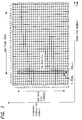
- FIG. 1 shows how to construct slots of the transmitting signal in this example, in which figure a vertical axis represents a frequency and a horizontal axis represents a time.
- orthogonal bases are provided by dividing the frequency axis and the time axis in a grid shape.
- one transmission band (one band slot) consists of 150 kHz and twenty-four subcaeriers are arranged within this one transmission band of 150 kHz.
- These twenty-four subcarriers are successively arranged at an equal interval of 6.25 kHz and to each subcarrier are given subcarrier numbers 0 to 23, respectively.
- really existing subcarriers are twenty-two ones from subcarrier numbers 1 to 22.
- the subcarrier numbers 0 and 23 at both ends within one band slot they are made guard band in which no subcarrier is arranged and their powers are made zero.
- one time slot having a time period of 200 ⁇ s is defined and at every time slot the twenty-two subcarriers are modulated by a burst signal for transmission.
- a time section in which twenty-five time slots are arranged is defined as one frame.
- To each time slot within this one frame is given time slot numbers 0 to 24, respectively.
- An area shown by hatching in FIG. 1 represents one time slot section of one band slot. Further, the time slot of the slot number 24 is made a time period where no data is transmitted.
- the multiple access in which the cell station communicates simultaneously with a plurality of the portable stations (terminal devices) is carried out.
- a mode of coupling to each portable station it is performed in such a manner as shown in FIGS. 2A to 2G.
- FIGS. 2A to 2G FIGS.
- FIG. 2A to 2G illustrate use of the time slots of six portable stations (users) U0,U1,U2, ..., U5 to be coupled to the cell station through one band slot (in practice, the band slot for use is switched by means of a frequency hopping described below), in which figure a time slot denoted by R is a receiving slot and denoted by T is a transmitting slot.
- the cell station establishes a frame timing of twenty-four time slot periods as shown in FIG. 2A (The last slot numbered 24 of twenty-five prepared time slots is not used.).
- the transmitting slot and the receiving slot are arranged here to use a different band transmission,respectively.
- the portable station U0 shown in FIG. 2B uses the time slots numbered 0, 6, 12, 18 within one frame as the receiving slot and uses the time slots numbered 3, 9, 15, 21 as the transmitting slot, through the respective time slots the reception or transmission of the burst signal being performed.
- the portable station U1 shown in FIG. 2C uses the time slots numbered 1, 7, 13, 19 within one frame as the receiving slot and uses the time slots numbered 4, 10, 16, 22 as the transmitting slot.
- the portable station U2 shown in FIG. 2D uses the times slots numbered 2, 8, 14, 20 within one frame as the receiving slot and uses the time slots numbered 5, 11, 17, 23 as the transmitting slot.
- TDMA Time Division Multiple Access
- a timing process and the process termed the frequency hopping are performed. That is, during about 200 ⁇ s before each transmitting slot T, a timing process TA in which a transmission timing is made to match with a timing of a signal from try base station side is performed. After a time passage of about 200 ⁇ s, when each transmitting slot T has been completed, the frequency hopping in which a band slot for the transmission and reception is switched over another band slot takes place.
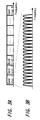
- a plurality of the band slots are assigned to one base station. For example, in case of the cellular system where one cell is comprised of one base station, if a band of 1.2MHz is allocated to one cell, eight band slots can be assigned to one cell. Likewise, if a band of 2.4 MHz is allocated to one cell,sixteen band slots can be assigned to one cell. Also, if a band of 4.8MHz is allocated to one cell, thirty-two band slots can be assigned to one cell. Finally, if a band of 9.6 MHz is allocated to one cell, sixty-four band slots can be assigned to one cell. In order to use equally a plurality of the band slots assigned to this one cell, the frequency switching process called the frequency hopping is carried out.
- FIGS. 3A and 3B show an example where eight band slots are arranged within one cell. At each of eight band slots prepared as shown in FIG. 3A, twenty-two subcarriers are arranged as shown in FIG. 3B for data transmission. Data is transmitted over each of the respective subcarriers under a ⁇ redetermined phase modulation.
- QPSK Quadrature Phase Shift Keying
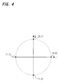
- data is transmitted as data at four points of phase position shifted in turn by ⁇ /2 of a circle on an orthogonal coordinate(a circle denoted by a broken line in FIG. 4) which are formed by laying an I component at right angels to a Q component, as is shown in FIG. 4.
- the transmitting signal is made such data as each subcarrier is multiplied by respective different random phase shift data. That is, at each of the twenty-two subcarriers from the subcarrier number 1 to the subcarrier number 22 within one band slot, an initial phase shift value of the first data of the first time slot of each frame is established and then the phase shift value is changed from the initial phase shift value in a sequence determined at random (This sequence is determined in advance.)
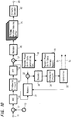
- FIG. 5 shows a receiving system of the terminal device, in which a received signal (This received signal is a signal which is subjected to a receiving process in a filter or an amplifier after received by an antenna.) available at an input terminal 11 is supplied to a mixer 12, where it is mixed with a frequency signal output by a frequency signal generator means 13 comprised of a PLL circuit(phase locked loop circuit) for frequency converting the received signal of a predetermined transmission band (band slot) into an intermediate frequency signal.
- this frequency signal generator means 13 had basically an output frequency which varies at an interval of one band slot (i.e. here at a interval of 150 kHz).
- the intermediate frequency signal output by the mixer 12 is supplied to an analogue/digital converter 14, where it is sampled at a predetermined sampling period.
- the received data sampled in the analogue/digital converter 14 is supplied to a window multiplier circuit 15, where it is multiplied by a window multiplying data (temporal wave form) corresponding to a window multiplying data by which it was multiplied on the transmitting side.
- the received data multiplied by the window multiplying data is supplied to a fast Fourier transform circuit(FFT circuit) 16, where it is subjected to a transforming process between a frequency axis and a time axis by the fast Fourier transform operation, thereby causing the data which modulated the twenty-two subcarriers at an interval of 6.25 kHz for transmission to be a single sequence of continuous data in the time axis.
- FFT circuit fast Fourier transform circuit
- the received data transformed into a single sequence is supplied to a multiplier 17, where it is multiplied by a random phase shift data output by a random phase shift data generator circuit 18.
- the random phase shift data output by the random phase shift data generator circuit 18 is generated on the basis of a pattern data stored in a random phase shift pattern storing memory 19.
- the random phase shift data is data for restoring the data whose phase was shifted and scattered on every subcarrier in transmission from the transmitting side (base station ) to the original data.
- an initial phase shift value of each subcarrier is determined and its value is arranged to change the phase to be shifted from the initial phase position at random (The order in which the phase shift amount is varied at random from the initial phase shift value is the same as that set up on the transmitting side).
- a timing to generate the random phase shift data by the generator circuit 18 is set up under the control of a controller 25 which controls the receiving operation of this terminal device.
- the data whose phase has been restored to original phase is supplied to a decoder 20, where the phase modulated data is decoded by the differential demodulation or the like.
- the decoded data is supplied to a four frame deinterleave buffer 21, where interleaved data over four frames in transmission is restored to data of original sequence.
- the deinterleaved data is supplied to a Viterbi decoder circuit 22 for Viterbi decoding.
- the Viterbi decoded data is then supplied as the received data to a received data processing circuit (not shown) at subsequent stage from a received data output terminal 23.
- the decoded data by the decoder 20 is supplied to a decision circuit 24 which decides whether or not the data has correctly been decoded and supplies the decision data to the controller 25.
- this decision for example, when accumulating phases of the signal over a time period in which data of the twenty-two subcarriers forming one band slot time period is acquired, if the accumulated phases vary at an angular interval of about ⁇ /2, the decision data is made what indicates that the decoding has been completed correctly. If the accumulated phases do not vary at the angular interval of about ⁇ /2, the decision data is made what indicates that it is erroneously processed data.
- the fine adjustment of the received frequency can be implemented by such processings as changing the output frequency of the frequency signal generator means 13 at an interval of 6.25kHz, or as establishing the number of transform points in the fast Fourier transform by FFT circuit 16 more than the number of the subcarriers (twenty-two subcarriers) forming one band slot and then changing a position of the twenty-two subcarriers extracted from the transform points as a sequence of data or the like. Furthermore,the fine adjustment of the received frequency may be performed by other processing.
- the controller 25 in the present embodiment outputs a frame position detecting data D 2 based on a timing when a predetermined condition has been decided by the decision circuit 24. On the basis of the frame position detecting data D 2 , a processing timing at each of the circuits within the terminal device is set for the timing synchronous with the received data.
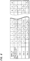
- FIG. 6 shows an example of the initial phase shift amounts of respective subcarriers.
- Phase shift value of transmitting data therein shows the initial phase shift amount of each of the subcarriers in each frame. Its value is determined in turn from the carrier number 0.
- These phase shift values are here set up within a range from - ⁇ to ⁇ so that all of them will be different phase shift amounts at respective subcarriers within one bans slot.
- FIG. 7 is a diagram which shows the initial phase shift values of the respective carrier numbers by its phase state, in which figure the phases of the carrier numbers are represented as #0, #1, #2 and so on.
- the initial phase shift amounts are set up according to case 1 and in the following frame the initial phase shift amounts are set up according to case 2 where they are shifted by one subcarrier. In the further following frame, the initial phase shift amounts are set up according to case 3 where they are shifted further by one subcarrier.
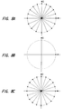
- the transmitting data is scattered values and so the phase states corresponding to cases 1, 2 and 3 will changes as shown in FIGS. 9A, 9B and 9C.
- the accumulated phases in the decision circuit 24 correspond to case 2, it is decided that they change at an angular unit of about ⁇ /2 and the decision data indicating that the correct decoding has been performed is then supplied to the controller 25.
- the decision data indicating that the data has been erroneously processed is supplied to the controller 25.
- the controller 25 outputs the frequency offset correction data D, and makes the initial phase shift to change in turn in order to control the receiving frequency to be set up correctly, until the state of case 2 is defected.
- the random phase shift pattern used for the first slot in a frame is produced by the random phase shift data generator means 18 and then the output of the decoder of received signal is multiplied by that random phase shift pattern, if it is decided that the phases of the respective subcarriers vary at an angular unit of about ⁇ /2, then it can be determined that the slot is the first slot in the frame.
- the timing of the frame can be defected by processing in this way.
- a slot signal in a certain slot is stored in a memory 31 and this signal is multiplied by the first shift pattern of the frame, by the second shift pattern of the frame, by the third shift pattern of the frame, etc.
- results of the multiplication by the respective shift patterns are decided, thereby also allowing the slot number in the frame given to the relevant slot to be estimated.
- received data transformed by the fast Fourier transform circuit(FFT circuit) 16 is supplied to the multiPlier 17 which multiplies the received data by the phase shift data output by the random phase shift data generator circuit 18.
- the received data transformed by the FFT circuit is supplied to a memory 31 and after it is once stored, it is supplied to a multiplier 32 which multiplies it by the phase shift data output from the random phase shift data generator circuit 18.
- a timing of outputting the phrase shift data from the random phase shift data generator circuit 18 to the multiplier 32 is made to synchronize with a timing of reading the received data out of the memory 31.
- a memory of a capacity which is capable of storing the received data for a predetermined time period e.g. one frame period or one slot time period ) is used.
- a timing of reading the data out of the memory 31 is controlled by a controller 35.
- a multiplied output of the multiplier 32 is decoded by a decoder 33.
- This decoder 33 has the same structure as that of the decoder 20 which decodes the output of the multiplier 17.
- the data decoded by the decoder 33 is supplied to a decision circuit 34 which decides if the data is correctly decoded and its decision data is then supplied to the controller 35.
- this decision for example, when accumulating phases of signal over a time period in which data of the twenty-two subcarriers forming one band slot time period is acquired, if the accumulated phases vary at the angular of about ⁇ /2, the decision data is made what indicates that the decoding has been completed correctly. If the accumulated phases do not vary at the angular unit of about ⁇ /2, the decision data is made what indicates that it is erroneously processed data.
- the controller 35 estimates, if it receives the decision data indicating that the correct decoding has been completed, that there is no frequency offset in the received signal at that time. When the decision data indicating that the correct decoding can not be performed, it is decided that there is a frequency offset in the received data at that time. On the basis of a result of the decision, the controller 35 outputs the frequency offset correction data D 1 and makes a fine adjustment of a received frequency at an interval of 6,25 kHz.
- the second embodiment by using the received data once stored in the memory 31, it is possible to perform processings for the received frequency offset detection aid the frame position detection irrespective of the actual receiving condition.
- the minimum unit of data required for detecting the frequency offset and the frame position is stored in the memory 31, it is possible that the stored data is repeatedly read out and at every readout time the initial phase shift amount is shifted in turn as case 1, 2 and 3 shown in FIG. 6, the result of decoding by the decoder 33 being decided in the decision circuit 34 for detecting the frequency offset and the frame position.
- the received data stored in the memory 31 it is possible to quickly detect the frequency offset and the frame position.
- the present invention is of course applicable to a case where a signal transmitted from the terminal device is received at the cell station.
- the detected offset value is reported to the terminal apparatus with which the base station is communicating, and the terminal apparatus adjusts the frequency offset of a signal from itself in accordance with the report.
- the phase shift amount is set up at random within the range from - ⁇ to ⁇ , whereas the phase shift amount may be set up at random within the other range. For example, it may be set up at random within the range from 0 to ⁇ /2.
- the present invention is applied to the multicarrier signal transmission system described referring to FIG. 1 to FIG. 4.
- the present invention is also applicable to a communication method and its receiving apparatus to which various transmission systems of other signal are applied.
- the specific modulating method and encoding method they are not limited to respective those of the embodiments described above.
- the mode of communication to be applied it is applicable to the case where the multicarrier signal is transmitted in various wireless communications other than the wireless telephone system described above on its embodiment.
- an initial phase of each of subcarriers forming multicarrier signal is set to a predetermined random value, it is possible to precisely receive the transmitted multicarrier signal by detecting the random initial phase on the reception side.
- the frequency offset between the transmission band and the reception band of the reception signal is detected by detecting an initial phase shift amount of each of subcarriers. it is possible to precisely correct the frequency offset.
- the reception apparatus of the present invention since the frequency offset between the transmission band and the reception band of the reception signal is determined based on the phase change between the subcarriers determined by the determining means, it is possible to detect the frequency offset of the multicarrier signal with a simple arrangement.
- the phase shift data based on the initial phase previously set for each of the subcarriers is multiplied with each of the subcarriers of the received signal, and the multiplied signal is decoded by the determining means. Then, it is determined whether or not the phase change falls in a predetermined state. Therefore, it is possible to easily determine whether or not the frequency is offset, only by determining the result of the decoding processing.
- the multiplying means successively shifts the arrangement of the phase data to be multiplied with each of the subcarriers and a position where the determining means determines a predetermined state is determined, it is possible to easily detect a reception position with no frequency offset.
Landscapes
- Engineering & Computer Science (AREA)
- Signal Processing (AREA)
- Computer Networks & Wireless Communication (AREA)
- Mobile Radio Communication Systems (AREA)
- Synchronisation In Digital Transmission Systems (AREA)
Applications Claiming Priority (3)
| Application Number | Priority Date | Filing Date | Title |
|---|---|---|---|
| JP348803/96 | 1996-12-26 | ||
| JP34880396 | 1996-12-26 | ||
| JP34880396A JP3684727B2 (ja) | 1996-12-26 | 1996-12-26 | 通信方法及び受信装置 |
Publications (2)
| Publication Number | Publication Date |
|---|---|
| EP0851641A2 true EP0851641A2 (de) | 1998-07-01 |
| EP0851641A3 EP0851641A3 (de) | 2001-03-21 |
Family
ID=18399478
Family Applications (1)
| Application Number | Title | Priority Date | Filing Date |
|---|---|---|---|
| EP97122797A Withdrawn EP0851641A3 (de) | 1996-12-26 | 1997-12-23 | Kommunikationsverfahren und Empfangsvorrichtung für OFDM-Systeme |
Country Status (4)
| Country | Link |
|---|---|
| US (1) | US5903614A (de) |
| EP (1) | EP0851641A3 (de) |
| JP (1) | JP3684727B2 (de) |
| KR (1) | KR19980064534A (de) |
Cited By (1)
| Publication number | Priority date | Publication date | Assignee | Title |
|---|---|---|---|---|
| WO2000033496A1 (en) * | 1998-12-01 | 2000-06-08 | Samsung Electronics Co., Ltd. | Frequency synchronizing device for ofdm/cdma system |
Families Citing this family (32)
| Publication number | Priority date | Publication date | Assignee | Title |
|---|---|---|---|---|
| FR2764143A1 (fr) * | 1997-05-27 | 1998-12-04 | Philips Electronics Nv | Procede de determination d'un format d'emission de symboles dans un systeme de transmission et systeme |
| KR100655952B1 (ko) * | 1998-02-26 | 2006-12-08 | 소니 가부시끼 가이샤 | 통신시스템, 기지국장치, 통신단말장치 및 통신방법 |
| WO2000003508A1 (fr) * | 1998-07-13 | 2000-01-20 | Sony Corporation | Procede de communication, emetteur, et recepteur |
| US6317470B1 (en) * | 1998-09-15 | 2001-11-13 | Ibiquity Digital Corporation | Adaptive weighting method for orthogonal frequency division multiplexed soft symbols using channel state information estimates |
| US6278685B1 (en) | 1999-08-19 | 2001-08-21 | Intellon Corporation | Robust transmission mode |
| US6961369B1 (en) * | 1999-11-09 | 2005-11-01 | Aware, Inc. | System and method for scrambling the phase of the carriers in a multicarrier communications system |
| US6442129B1 (en) | 1999-12-06 | 2002-08-27 | Intellon Corporation | Enhanced channel estimation |
| US6397368B1 (en) | 1999-12-06 | 2002-05-28 | Intellon Corporation | Forward error correction with channel adaptation |
| US6289000B1 (en) | 2000-05-19 | 2001-09-11 | Intellon Corporation | Frame control encoder/decoder for robust OFDM frame transmissions |
| US20020067772A1 (en) * | 2000-06-28 | 2002-06-06 | Shepperd Michael B. | Method and system for sending information over metal wire |
| US7352770B1 (en) * | 2000-08-04 | 2008-04-01 | Intellon Corporation | Media access control protocol with priority and contention-free intervals |
| US7298691B1 (en) | 2000-08-04 | 2007-11-20 | Intellon Corporation | Method and protocol to adapt each unique connection in a multi-node network to a maximum data rate |
| US6907044B1 (en) | 2000-08-04 | 2005-06-14 | Intellon Corporation | Method and protocol to support contention-free intervals and QoS in a CSMA network |
| US6987770B1 (en) | 2000-08-04 | 2006-01-17 | Intellon Corporation | Frame forwarding in an adaptive network |
| US6909723B1 (en) | 2000-08-04 | 2005-06-21 | Intellon Corporation | Segment bursting with priority pre-emption and reduced latency |
| US7469297B1 (en) | 2000-08-04 | 2008-12-23 | Intellon Corporation | Mechanism for using a quasi-addressed response to bind to a message requesting the response |
| US7826466B2 (en) * | 2002-06-26 | 2010-11-02 | Atheros Communications, Inc. | Communication buffer scheme optimized for VoIP, QoS and data networking over a power line |
| US8149703B2 (en) * | 2002-06-26 | 2012-04-03 | Qualcomm Atheros, Inc. | Powerline network bridging congestion control |
| US7120847B2 (en) * | 2002-06-26 | 2006-10-10 | Intellon Corporation | Powerline network flood control restriction |
| EP1554848A4 (de) | 2002-10-21 | 2010-03-03 | Intellon Corp | Staufreie zugriffsintervalle in einem csma-netzwerk |
| US7281187B2 (en) | 2003-11-20 | 2007-10-09 | Intellon Corporation | Using error checking bits to communicated an address or other bits |
| US8090857B2 (en) | 2003-11-24 | 2012-01-03 | Qualcomm Atheros, Inc. | Medium access control layer that encapsulates data from a plurality of received data units into a plurality of independently transmittable blocks |
| US7660327B2 (en) * | 2004-02-03 | 2010-02-09 | Atheros Communications, Inc. | Temporary priority promotion for network communications in which access to a shared medium depends on a priority level |
| US7715425B2 (en) * | 2004-02-26 | 2010-05-11 | Atheros Communications, Inc. | Channel adaptation synchronized to periodically varying channel |
| WO2005088853A1 (en) | 2004-03-09 | 2005-09-22 | Neocific Inc. | Methods and apparatus for random access in multi-carrier communication systems |
| US7636370B2 (en) * | 2005-03-03 | 2009-12-22 | Intellon Corporation | Reserving time periods for communication on power line networks |
| US7822059B2 (en) | 2005-07-27 | 2010-10-26 | Atheros Communications, Inc. | Managing contention-free time allocations in a network |
| US8175190B2 (en) | 2005-07-27 | 2012-05-08 | Qualcomm Atheros, Inc. | Managing spectra of modulated signals in a communication network |
| WO2008141165A1 (en) * | 2007-05-10 | 2008-11-20 | Intellon Corporation | Managing distributed access to a shared medium |
| US8781016B2 (en) | 2010-04-12 | 2014-07-15 | Qualcomm Incorporated | Channel estimation for low-overhead communication in a network |
| US8891605B2 (en) | 2013-03-13 | 2014-11-18 | Qualcomm Incorporated | Variable line cycle adaptation for powerline communications |
| US9621197B2 (en) | 2015-03-10 | 2017-04-11 | Samsung Electronics Co., Ltd. | Bi-phased on-off keying (OOK) transmitter and communication method |
Family Cites Families (9)
| Publication number | Priority date | Publication date | Assignee | Title |
|---|---|---|---|---|
| US3742498A (en) * | 1970-05-06 | 1973-06-26 | Itt | Synchronization and position location system |
| US4041391A (en) * | 1975-12-30 | 1977-08-09 | The United States Of America As Represented By The Administrator Of The National Aeronautics And Space Administration | Pseudo noise code and data transmission method and apparatus |
| CA1191905A (en) * | 1982-06-30 | 1985-08-13 | Canadian Patents And Development Limited/Societe Canadienne Des Brevets Et D'exploitation Limitee | Spread spectrum modem |
| US5029184A (en) * | 1990-01-24 | 1991-07-02 | Harris Corporation | Low probability of intercept communication system |
| FR2719382B1 (fr) * | 1994-05-02 | 1996-05-31 | Thomson Csf | Procédé de détection radar discrète et système de mise en Óoeuvre. |
| US5677927A (en) * | 1994-09-20 | 1997-10-14 | Pulson Communications Corporation | Ultrawide-band communication system and method |
| JP3421880B2 (ja) * | 1994-10-05 | 2003-06-30 | ソニー株式会社 | 復調装置 |
| JP3371175B2 (ja) * | 1994-11-15 | 2003-01-27 | ソニー株式会社 | 伝送方式 |
| US5682376A (en) * | 1994-12-20 | 1997-10-28 | Matsushita Electric Industrial Co., Ltd. | Method of transmitting orthogonal frequency division multiplex signal, and transmitter and receiver employed therefor |
-
1996
- 1996-12-26 JP JP34880396A patent/JP3684727B2/ja not_active Expired - Fee Related
-
1997
- 1997-12-23 EP EP97122797A patent/EP0851641A3/de not_active Withdrawn
- 1997-12-23 KR KR1019970072783A patent/KR19980064534A/ko not_active Withdrawn
- 1997-12-24 US US08/998,386 patent/US5903614A/en not_active Expired - Fee Related
Cited By (1)
| Publication number | Priority date | Publication date | Assignee | Title |
|---|---|---|---|---|
| WO2000033496A1 (en) * | 1998-12-01 | 2000-06-08 | Samsung Electronics Co., Ltd. | Frequency synchronizing device for ofdm/cdma system |
Also Published As
| Publication number | Publication date |
|---|---|
| JP3684727B2 (ja) | 2005-08-17 |
| EP0851641A3 (de) | 2001-03-21 |
| US5903614A (en) | 1999-05-11 |
| KR19980064534A (ko) | 1998-10-07 |
| JPH10190611A (ja) | 1998-07-21 |
Similar Documents
| Publication | Publication Date | Title |
|---|---|---|
| US5903614A (en) | Communication method and receiving apparatus | |
| US5914932A (en) | Communication method and receiving apparatus | |
| EP0706273B1 (de) | Verfahren und Einrichtung zur Demodulation eines auf mehreren Trägern übermittelten Signals | |
| US6993084B1 (en) | Coarse frequency synchronisation in multicarrier systems | |
| EP0847643B1 (de) | Verfahren zur vereinfachung der demodulation in einem mehrfachträger-übertragungssystem | |
| US6347120B1 (en) | Communication method, transmitter, receiver, and cellular radio communication system | |
| US5276706A (en) | System and method for minimizing frequency offsets between digital communication stations | |
| US6088406A (en) | Reception method, reception apparatus and timing detecting apparatus | |
| US6195534B1 (en) | Communication method, transmitter, receiver, wherein subcarriers are used to transmit digital header and message data in a cellular radio communications system | |
| EP0884878A2 (de) | Synchronisierung von Rahmen, Symboltakt und Träger in Mehträgerempfängern | |
| JP2879030B2 (ja) | Ofdm送信装置及び受信装置とofdm送信方法及び受信方法 | |
| EP0901260A2 (de) | Synchronisation von Rahmen und Symbolen in Mehrträgerempfängern | |
| KR100666165B1 (ko) | 무선통신방법 및 무선통신 시스템 | |
| KR100355727B1 (ko) | 반송주파수를전환하는주파수호핑통신방법및장치 | |
| KR20010101351A (ko) | 이중 검출 임계값을 사용하여 동기화를 포착하는 시스템및 방법 | |
| US6047023A (en) | Swept frequency modulation and demodulation technique | |
| KR20010032995A (ko) | 대역-확산 디지털 송신을 위한 병렬 상관기를 갖는 수신기 | |
| EP0915629B1 (de) | Kommunikationsendgerät, zellulares Funkkommunikationssystem und Informationsübertragungsverfahren | |
| US6195341B1 (en) | Communication method, base station and terminal apparatus | |
| JP2001053713A (ja) | マルチキャリア信号送信装置及びマルチキャリア信号受信装置 | |
| KR100641067B1 (ko) | 제 2 트랜시버와 통신하기 위한 트랜시버 및 방법과, 무선 전화 시스템 | |
| JP2001148681A (ja) | 無線通信システム | |
| JP2772287B2 (ja) | Ofdm復調装置 | |
| JP2000138647A (ja) | ディジタル伝送装置 | |
| JP4041196B2 (ja) | 無線接続形成方法および該方法を実施するための移動ステーション |
Legal Events
| Date | Code | Title | Description |
|---|---|---|---|
| PUAI | Public reference made under article 153(3) epc to a published international application that has entered the european phase |
Free format text: ORIGINAL CODE: 0009012 |
|
| AK | Designated contracting states |
Kind code of ref document: A2 Designated state(s): DE FI FR GB NL |
|
| AX | Request for extension of the european patent |
Free format text: AL;LT;LV;MK;RO;SI |
|
| PUAL | Search report despatched |
Free format text: ORIGINAL CODE: 0009013 |
|
| AK | Designated contracting states |
Kind code of ref document: A3 Designated state(s): AT BE CH DE DK ES FI FR GB GR IE IT LI LU MC NL PT SE |
|
| AX | Request for extension of the european patent |
Free format text: AL;LT;LV;MK;RO;SI |
|
| 17P | Request for examination filed |
Effective date: 20010726 |
|
| AKX | Designation fees paid |
Free format text: DE FI FR GB NL |
|
| 17Q | First examination report despatched |
Effective date: 20031217 |
|
| STAA | Information on the status of an ep patent application or granted ep patent |
Free format text: STATUS: THE APPLICATION IS DEEMED TO BE WITHDRAWN |
|
| 18D | Application deemed to be withdrawn |
Effective date: 20040428 |