EP0901260A2 - Synchronisation von Rahmen und Symbolen in Mehrträgerempfängern - Google Patents
Synchronisation von Rahmen und Symbolen in Mehrträgerempfängern Download PDFInfo
- Publication number
- EP0901260A2 EP0901260A2 EP98303624A EP98303624A EP0901260A2 EP 0901260 A2 EP0901260 A2 EP 0901260A2 EP 98303624 A EP98303624 A EP 98303624A EP 98303624 A EP98303624 A EP 98303624A EP 0901260 A2 EP0901260 A2 EP 0901260A2
- Authority
- EP
- European Patent Office
- Prior art keywords
- signal
- frame
- symbol
- division multiplex
- frequency division
- Prior art date
- Legal status (The legal status is an assumption and is not a legal conclusion. Google has not performed a legal analysis and makes no representation as to the accuracy of the status listed.)
- Withdrawn
Links
Images


Classifications
-
- H—ELECTRICITY
- H04—ELECTRIC COMMUNICATION TECHNIQUE
- H04L—TRANSMISSION OF DIGITAL INFORMATION, e.g. TELEGRAPHIC COMMUNICATION
- H04L27/00—Modulated-carrier systems
- H04L27/26—Systems using multi-frequency codes
- H04L27/2601—Multicarrier modulation systems
- H04L27/2647—Arrangements specific to the receiver only
- H04L27/2655—Synchronisation arrangements
- H04L27/2656—Frame synchronisation, e.g. packet synchronisation, time division duplex [TDD] switching point detection or subframe synchronisation
-
- H—ELECTRICITY
- H04—ELECTRIC COMMUNICATION TECHNIQUE
- H04L—TRANSMISSION OF DIGITAL INFORMATION, e.g. TELEGRAPHIC COMMUNICATION
- H04L27/00—Modulated-carrier systems
- H04L27/26—Systems using multi-frequency codes
- H04L27/2601—Multicarrier modulation systems
- H04L27/2647—Arrangements specific to the receiver only
- H04L27/2655—Synchronisation arrangements
- H04L27/2662—Symbol synchronisation
-
- H—ELECTRICITY
- H04—ELECTRIC COMMUNICATION TECHNIQUE
- H04L—TRANSMISSION OF DIGITAL INFORMATION, e.g. TELEGRAPHIC COMMUNICATION
- H04L27/00—Modulated-carrier systems
- H04L27/26—Systems using multi-frequency codes
- H04L27/2601—Multicarrier modulation systems
- H04L27/2647—Arrangements specific to the receiver only
- H04L27/2655—Synchronisation arrangements
- H04L27/2668—Details of algorithms
- H04L27/2673—Details of algorithms characterised by synchronisation parameters
- H04L27/2676—Blind, i.e. without using known symbols
-
- H—ELECTRICITY
- H04—ELECTRIC COMMUNICATION TECHNIQUE
- H04L—TRANSMISSION OF DIGITAL INFORMATION, e.g. TELEGRAPHIC COMMUNICATION
- H04L7/00—Arrangements for synchronising receiver with transmitter
- H04L7/04—Speed or phase control by synchronisation signals
- H04L7/041—Speed or phase control by synchronisation signals using special codes as synchronising signal
- H04L2007/045—Fill bit or bits, idle words
-
- H—ELECTRICITY
- H04—ELECTRIC COMMUNICATION TECHNIQUE
- H04L—TRANSMISSION OF DIGITAL INFORMATION, e.g. TELEGRAPHIC COMMUNICATION
- H04L7/00—Arrangements for synchronising receiver with transmitter
- H04L7/04—Speed or phase control by synchronisation signals
- H04L7/08—Speed or phase control by synchronisation signals the synchronisation signals recurring cyclically
Definitions
- the present invention relates to a demodulating apparatus and a demodulating method for demodulating a digital orthogonal frequency division multiplex modulated signal in which an information signal modulates a plurality of carriers whose frequency components are in an orthogonal relationship with one another.
- a demodulating apparatus for demodulating a digital orthogonal frequency division multiplex modulated signal in which an information signal modulates a plurality of carriers whose frequency components are in an orthogonal relationship with one another there is proposed a demodulating apparatus for an OFDM (Orthogonal Frequency Division Multiplex) modulated signal (hereinafter referred to merely as an OFDM modulated signal) which is adopted by a DAB (Digital Audio Broadcasting), etc. taking place in Europe.
- OFDM Orthogonal Frequency Division Multiplex
- a modulated signal using a multiplicity of carriers whose frequency components are in an orthogonal relationship with one another encodes data such as audio data or the like, and the encoded data are allocated to each carrier, thereby modulating each carrier, a digital signal in frequency domain comprised of each modulated carrier is inverse fast Fourier transformed into a digital signal in a time domain, and the digital signal in the time domain is D/A converted.
- A/D converting such an OFDM modulated signal and then applying the fast Fourier transform to the A/D converted signal the encoded data allocated to each carrier is obtained.
- each carrier is subjected to a QPSK (Quadrature Phase Shift Keying) modulation, so that this modulation is called an OFDM - QPSK.
- QPSK Quadrature Phase Shift Keying
- This transmissive unit is termed a symbol.
- a collection of seventy-six symbols is termed a frame.
- mode 3 a collection of one hundred and fifty-three symbols is termed a frame.
- a null symbol is not included in the number of symbols in one frame.
- a carrier indicated by zero is one with a central frequency (a period of that carrier is T).
- Data amount of one symbol is 1536 waves, its data amount is 1536 x 2 bits, i.e. 48 CU (Capacity unit) x 64 bits.
- each symbol of the DAB signal differs depending on the mode.
- the duration of each symbol in mode 2 is 1/4 of the duration of each symbol in mode 1.
- the duration of each symbol in mode 3 is 1/8 of that of each symbol in mode 1.
- the duration of each symbol in mode 4 is 1/2 of that of each symbol in mode 1.
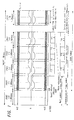
- a DAB signal (shown in FIG. 3A) from a receiving antenna 1 is supplied to a RF (radio frequency) amplifier/frequency converter/IF (intermediate frequency) amplifier 2 where it is RF amplified, frequency converted and IF amplified for obtaining an OFDM modulated signal of baseband, and the OFDM modulated signal is supplied to an A/D converter 3 where it is converted into a time series of digital data.
- RF radio frequency
- IF intermediate frequency
- the time series of digital data from the A/D converter 3 is supplied to a time synchronizing signal generator 7 which generates a time synchronizing signal for every symbol.
- the time synchronizing signal is supplied to a fast Fourier transform circuit 4 and a data decoder 5 for controlling the fast Fourier transform timing as well as controlling each circuit in the data decoder 5 to be synchronized.
- the intermediate frequency signal from the RF amplifier/frequency converter/IF amplifier 2 is supplied to a null detector (envelope detector circuit) 8 which produces a null detecting signal (see FIG. 3B).
- This null detecting signal is supplied to a frame synchronizing signal generator 9.
- the frame synchronizing signal generator 9 is a pulse oscillator which generates the frame synchronizing signal. So, it is necessary to make it synchronized with the null detecting signal (FIG. 3B) of the first or second frame of the DAB signal. Thus, by making the frame synchronizing signal generator 9 synchronized with a starting (falling) time point of the null detecting signal, the frame synchronizing signal generator 9 will thereafter issue a frame synchronizing signal (see FIG. 3C) corresponding with the starting time point of the null symbol.
- the frame synchronizing signal is supplied to the fast Fourier transform circuit 4 in which a frame window signal (FIG. 3D) during a frame period except the null symbol is produced.
- the time series of digital data from the A/D converter 3 is supplied to the fast Fourier transform circuit 4 where it is converted into a frequency sequence of digital data.
- the frequency sequence of digital data from the fast Fourier transform circuit 4 is supplied to the data decoder 5 for decoding and decoded data is output to an output terminal 6.
- the data decoder 5 is comprised of a frequency deinterleave circuit, a time deinterleave circuit and an error correcting circuit, which are sequentially cascaded.
- the frame synchronizing signal generator is made synchronized with the null detecting signal, when the starting time point of the null detecting signal deviates greatly from the null symbol of DAB signal due to fading or decrease of S/N ratio of the DAB signal, the frame synchronizing signal from the frame synchronizing signal generator also deviates from the starting time point of the null symbol of DAB signal.
- the timing of the frame window signal produced in the fast Fourier transform circuit 4 will deviate from the frame period except the null symbol of DAB signal. If an amount of the deviation is large, it will be impossible to estimate the TFPR (Time Frequency Phase Reference) symbol following the null symbol, and besides, it will be necessary to make the frame synchronizing signal generator 9 synchronized over again.
- TFPR Time Frequency Phase Reference
- the present invention aims to provide, in a demodulating apparatus comprising a time synchronizing signal generator means for receiving a digital orthogonal frequency division multiplex modulated signal in which an information signal modulates a plurality of carriers whose frequency components are in the orthogonal relationship with one another and for generating a time synchronizing signal synchronized with a symbol forming each frame of the digital orthogonal frequency division multiplex modulated signal, a frame synchronizing signal generator means for generating a frame synchronizing signal synchronized with each frame of the digital orthogonal frequency division multiplex modulated signal and the fast Fourier transform means for receiving the digital orthogonal frequency division multiplex modulated signal, the frame synchronizing signal and the time synchronizing signal and for fast Fourier transforming the digital orthogonal frequency division multiplex modulated signal, where in a demodulated digital information signal may be obtained from the fast Fourier transform means, such one in which, without any influences of the fading or the decrease of S/N ratio of the received digital orthogonal frequency
- the present invention aims to provide, in a demodulating apparatus comprising a time synchronizing signal generator means for receiving the digital orthogonal frequency division multiplex modulated signal in which an information signal modulates a plurality of carriers whose frequency components are in the orthogonal relationship with each other and each frame of which is comprised of the null symbol, the synchronization symbol and the plurality of subsequent symbols and for generating a time synchronizing signal synchronized with the symbol forming each frame of the digital orthogonal frequency division multiplex modulated signal, a frame synchronizing signal generator means for generating the frame synchronizing signal synchronized with each frame of the digital orthogonal frequency division multiplex modulated signal, and the fast Fourier transform means for receiving the digital orthogonal frequency division multiplex modulated signal, the frame synchronizing signal and the time synchronizing signal and for fast Fourier transforming the digital orthogonal frequency division multiplex modulated signal to obtain a demodulated digital information signal, and in which a window signal used in the fast Fourier transform means for the synchronization symbol
- the present invention aims to provide, in a demodulating method wherein the basis of time synchronizing signal synchronized with the symbol forming each frame of the digital orthogonal frequency division multiplex modulated signal, the frame synchronizing digital orthogonal frequency division multiplex modulated signal, is generated, and the digital orthogonal frequency division multiplex modulated is fast-Fourier-transformed by using the frame synchronizing signal and the time synchronizing signal to obtain a demodulated digital information signal, such one that without any influences of the fading or the decrease of S/N ratio at the received digital orthogonal frequency division multiplex modulated signal, the frame synchronizing signal synchronized at high accuracy with each frame of the orthogonal frequency division multiplex modulated signal can be acquired from the frame synchronizing generator.
- the present invention aims to provide, in a demodulating method wherein the time synchronizing signal synchronized with the symbol forming each frame of the digital orthogonal frequency division multiplex modulated signal comprising the steps of generating based on the digital orthogonal frequency division multiplex modulated signal in which an information signal modulates a plurality of carriers whose frequency components are in the orthogonal relationship with each other and each frame of which is comprised of the null symbol, the synchronization symbol and the plurality of subsequent symbols is generated, the digital frequency division multiplex modulated signal is fast-Fourier-transformed by using the frame synchronizing signal and the time synchronizing signal, and the window signal used in the fast Fourier transform for the synchronization symbol and the plurality of subsequent symbols is generated on the basis of frame synchronization signal, such one that wherein, without any influences at the fading or the fading of S/N ratio of the received digital orthogonal frequency division multiplex modulated signal, the window signal in the fast Fourier transform synchronization symbol and the plurality of subsequent symbols of
- the present invention provides a demodulating apparatus having a time synchronizing signal generator means for receiving the digital orthogonal frequency division multiplex modulated signal in which an information signal modulates a plurality of carriers whose frequency components are in the orthogonal relationship with each other and for generating a time synchronizing signal synchronized with the symbols forming each frame of the digital orthogonal frequency division multiplex modulated signal, a frame synchronizing signal generator means for generating the frame synchronizing signal synchronized with each frame of the digital orthogonal frequency division multiplex modulated signal, and a fast Fourier transform means for receiving the digital orthogonal frequency division multiplex modulated signal, the frame synchronizing signal and the time synchronizing signal, and for fast Fourier transforming the digital orthogonal frequency division multiplex modulated signal to obtain a demodulated digital information signal from the fast Fourier transform means, wherein, there are provided, correlation detector means for detecting a correlation between a guard section of a symbol of the digital orthogonal frequency division multiplex modulated signal and a section having a correlation
- the correlation between the guard section of the digital orthogonal frequency division multiplex modulated signal and a section having a correlation with the guard section in the effective symbol of that symbol is detected by the correlation detector means.
- the detected output by the correlation detector means is section integrated with respect to the guard section.
- a peak of the triangular wave signal from the section integrator means is detected by the peak detector means.
- the frame timing signal of a predetermined frame of each of the frames is produced by the frame timing signal producing means based on the peak detecting signal from the peak detector means.
- the frame synchronizing signal generator means is made synchronized by the frame timing signal from the frame timing.
- the received signal from the receiving antenna 1 is supplied to the RF (radio frequency) amplifier/ frequency converter/IF (intermediate frequency) amplifier 2, where it is RF amplified, frequency converted and IF amplified, respectively.
- RF radio frequency
- IF intermediate frequency
- the time series of digital data from the A/D converter 3 is supplied to the fast Fourier transform circuit 4, where it is transformed into the frequency sequence of digital data.
- the frequency sequence of digital data from the fast Fourier transform circuit 4 is supplied to the data decoder 5 for decoding and the decoded data is output on the output terminal 6.
- the data decoder 5 is made up of the frequency deinterleave circuit, the time deinterleave circuit and the error correction circuit which are sequentially cascaded.
- the time sequence of digital data from the A/D converter 3 is supplied to the time synchronizing signal generator 7 and the time synchronizing signal obtained therefrom at the symbol of each frame is supplied to the fast Fourier transform circuit 4 and to the data decoder 5 for controlling the fast Fourier transform timing as well as controlling each circuit in the data decoder 5 for synchronization.
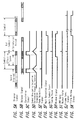
- the intermediate frequency signal from the RF amplifier/frequency converter /IF amplifier 2 is supplied to the null detector (envelope detector circuit) 8 for obtaining the null detecting signal (see FIG. 5F).
- the null detecting signal is supplied to a window signal generator 15 for generating a window signal (see FIG. 5H) which has one period (high level time period) including zero (low level) time period of the null detecting signal in FIG. 5F and spreading the zero time period before and after the same.
- each symbol in a frame of the digital data from the D/A converter 2 is comprised of the guard interval (guard section) in its head portion and the subsequent effective symbol. Furthermore, in the last portion of the effective symbol is provided a correlation period of time having a correlation with the guard interval in the same length of time as that of the guard interval.
- the digital data from the A/D converter 3 (FIG. 5A) is supplied directly to a correlation detector 11 and also to a delay device 10 having a time delay corresponding to a time period of the effective symbol.
- the delayed digital data (FIG. 5B) is supplied to the correlation detector 11 which detects a correlation between the two digital data. Further, the correlation detection is carried out by multiplying the original signal and the delayed signal together. By doing so, a correlation signal (FIG. 5C) which goes to a high level during a period corresponding to the correlation period of the original signal and the guard interval of the delayed signal is output from the correlation detector 11.
- the correlation signal from the correlation detector 11 is supplied to a section integrator 12 where it is integrated with respect to the guard interval.
- the section integrated signal of the correlation signal is, as shown in FIG. 5D, a triangular wave signal of line symmetry, which has a rising inclination during the correlation signal period and a falling inclination after completion of the correlation signal.
- the section integrated signal is supplied to a peak detector 13 for peak detection, where a peak detecting signal (FIG. 5E) indicative of a starting or finishing time of the symbol is output.
- the peak detecting signal is supplied to a null symbol start timing pulse generator 14 where a null symbol start timing pulse (FIG. 5G) of the first or second frame of the DAB signal is produced.
- the null symbol start timing pulse is a timing signal which is calculated from the time in the peak detecting signal and output by the timing pulse generator 14, and whose timing coincides with a starting timing of the null detecting signal.
- the null symbol start timing pulse will not coincide with the starting timing of the null detecting signal.
- the window signal (FIG. 5H) from the window signal generator 15 and the null symbol start timing pulse (FIG. 5G) are both supplied to an AND gate 16 which outputs an AND gate output pulse (FIG. 5I).
- the AND gate output pulse is supplied to the frame synchronizing signal generator 9 which is thereby made synchronized (FIG. 5J).
- the frame synchronizing signal (FIG. 5J) synchronized with the null symbol start timing pulse will be generated.
- the frame synchronizing signal is supplied to the fast Fourier transform circuit 4 in which a frame window signal (FIG. 5K) corresponding to a time period excepting the null symbol period from the frame period is produced.
- the demodulating apparatus comprising the time synchronizing signal generator means for receiving the digital orthogonal frequency division multiplex modulated signal in which an information signal modulates a plurality of carriers whose frequency components are in the orthogonal relationship with each other and for generating the time synchronizing signal synchronized with the symbol forming each frame of the digital orthogonal frequency division multiplex modulated signal
- the frame synchronizing signal generator means for generating the frame synchronizing signal synchronized with each frame of the digital orthogonal frequency division multiplex modulated signals and the fast Fourier transform means for receiving the digital orthogonal frequency division multiplex modulated signal, the frame synchronizing signal and the time synchronizing signal and for fast Fourier transforming the digital orthogonal frequency division multiplex modulated signal to obtain a demodulated digital information signal from the fast Fourier transform means
- the correlation detector means for detecting the correlation between the guard section of the symbol of the digital orthogonal frequency division multiplex modulated signal and a section having a correlation with the guard section in
- the demodulating apparatus comprising the time synchronizing signal generator means for the digital orthogonal frequency division multiplex modulated signal in which an information signal modulates a plurality of carriers whose frequency components are in the orthogonal relationship with each other and each frame of which is comprised of the null symbol, the synchronization symbol and the plurality of subsequent symbols, and for generating the time synchronizing signal synchronized with the symbol forming each frame of the digital orthogonal frequency division multiplex modulated signal
- the frame synchronizing signal generator means for generating the frame synchronizing signal synchronized with each frame of the digital orthogonal frequency division multiplex modulated signal
- the fast Fourier transform means for receiving the digital orthogonal frequency division multiplex modulated signal, the frame synchronizing signal and the time synchronizing signal and for fast Fourier transforming the digital orthogonal frequency division multiplex modulated signal to obtain the demodulated digital information signal in which the window signal used in the fast Fourier transform means for the synchronization symbol and the plurality of subsequent symbols may be
- the demodulating method in which, based on the digital orthogonal frequency division multiplex modulated signal wherein the information signal modulates the plurality of carriers whose frequency components are in the orthogonal relationship with each other, the time synchronizing signal synchronized with the symbols forming each frame of the digital orthogonal frequency division multiplex modulated signal is generated, generating the frame synchronizing signal synchronized with each frame of the digital orthogonal frequency division multiplex modulated signal is generated, and the digital orthogonal frequency division multiplex modulated signal is fast Fourier transformed by using the frame synchronizing signal and the time synchronizing signal to obtain the demodulated digital information signal, because the correlation between the guard section of the symbol of the digital orthogonal frequency division multiplex modulated signal and the section having a correlation with the guard section in the effective symbol of that symbol is detected, the detected output on the correlation is section integrated with respect to the guard section, a peak of the triangular wave signal which is the section integrated output is detected, the frame timing signal of the predetermined frame of
- the demodulating method in which based on the digital frequency orthogonal frequency division multiplex modulated signal in which an information signal modulates the plurality of carriers whose frequency components are in the orthogonal relationship with each other and each frame of which is comprised of the null symbol, the synchronization symbol and the plurality of subsequent symbols, the time synchronizing signal synchronized with the symbols forming each frame of the digital orthogonal frequency division multiplex modulated signal is generated, generating the frame synchronizing signal synchronized with each frame of the digital orthogonal frequency division multiplex modulated signal is generated, the digital orthogonal frequency division multiplex modulated signal is fast Fourier transformed by using the frame synchronizing signal and the time synchronizing signal, and the window signal used in the fast Fourier transform for the synchronization symbol and the plurality of subsequent symbols is generated on the basis of the frame synchronizing signal, because the correlation between the guard section of the symbol of the digital orthogonal frequency division multiplex modulated signal and the section having a correlation with the guard section in the
Landscapes
- Engineering & Computer Science (AREA)
- Computer Networks & Wireless Communication (AREA)
- Signal Processing (AREA)
- Synchronisation In Digital Transmission Systems (AREA)
Applications Claiming Priority (3)
| Application Number | Priority Date | Filing Date | Title |
|---|---|---|---|
| JP12096297 | 1997-05-12 | ||
| JP120962/97 | 1997-05-12 | ||
| JP9120962A JPH10313284A (ja) | 1997-05-12 | 1997-05-12 | 復調装置及び復調方法 |
Publications (2)
| Publication Number | Publication Date |
|---|---|
| EP0901260A2 true EP0901260A2 (de) | 1999-03-10 |
| EP0901260A3 EP0901260A3 (de) | 2002-03-20 |
Family
ID=14799318
Family Applications (1)
| Application Number | Title | Priority Date | Filing Date |
|---|---|---|---|
| EP98303624A Withdrawn EP0901260A3 (de) | 1997-05-12 | 1998-05-08 | Synchronisation von Rahmen und Symbolen in Mehrträgerempfängern |
Country Status (3)
| Country | Link |
|---|---|
| US (1) | US6192056B1 (de) |
| EP (1) | EP0901260A3 (de) |
| JP (1) | JPH10313284A (de) |
Cited By (10)
| Publication number | Priority date | Publication date | Assignee | Title |
|---|---|---|---|---|
| GB2353680A (en) * | 1999-08-27 | 2001-02-28 | Mitsubishi Electric Inf Tech | OFDM frame synchronisation |
| FR2821702A1 (fr) * | 2001-03-02 | 2002-09-06 | Canon Kk | Procede et dispositif de reception optimisee |
| EP1014636A3 (de) * | 1998-12-22 | 2002-10-23 | Nortel Networks Limited | Symbolsynchronisierung, Kanalschätzung und Verkürzung der Impulsantwort bei Mehrträgerempfängern |
| EP0980157A3 (de) * | 1998-08-10 | 2003-08-13 | Sony Corporation | Rahmensynchronisierung in einem DAB-Empfänger |
| EP1111867A3 (de) * | 1999-12-21 | 2003-12-10 | Matsushita Electric Industrial Co., Ltd. | Anfangserfassung und Frequenzsynchronisierung in Mehrträgersystemen |
| KR100411893B1 (ko) * | 2001-07-09 | 2003-12-24 | 한국전자통신연구원 | 직교 주파수 분할 다중화 수신 시스템의 심볼 동기 장치및 그 방법 |
| EP1387544A3 (de) * | 2002-07-05 | 2004-09-01 | British Broadcasting Corporation | Synchronisierung in Mehrträgerempfängern |
| EP1694019A1 (de) * | 2005-02-21 | 2006-08-23 | Samsung Electronics Co., Ltd. | Verfahren und System zur Kontrolle der Rahmensynchronisierung für den europäischen digitalen Tonrundfunk |
| EP1054540A3 (de) * | 1999-04-30 | 2006-11-02 | Sony Corporation | Verfahren, Vorrichtung und Empfänger zur Erkennung der Lage des Nullsymbols |
| WO2008047277A3 (en) * | 2006-10-16 | 2008-07-17 | Koninkl Philips Electronics Nv | Determining symbol synchronization information for ofdm signals |
Families Citing this family (24)
| Publication number | Priority date | Publication date | Assignee | Title |
|---|---|---|---|---|
| EP2254300B1 (de) | 1998-01-06 | 2013-05-15 | Mosaid Technologies Incorporated | System zur Mehrträgermodulation mit veränderbaren Symbolgeschwindigkeiten |
| JPH11252038A (ja) * | 1998-02-27 | 1999-09-17 | Sony Corp | デジタル放送の受信機 |
| JP2955285B1 (ja) * | 1998-09-30 | 1999-10-04 | 松下電器産業株式会社 | デジタルオーディオ受信機 |
| JP3606761B2 (ja) * | 1998-11-26 | 2005-01-05 | 松下電器産業株式会社 | Ofdm受信装置 |
| DE60029687T2 (de) | 1999-06-22 | 2007-10-18 | Matsushita Electric Industrial Co., Ltd., Kadoma | Symboltaktsynchronisierung in Mehrträgerempfängern |
| EP1073241A3 (de) * | 1999-07-29 | 2006-05-03 | Matsushita Electric Industrial Co., Ltd. | Synchronisieren von Symbolen bei Mehrträgerübertragung |
| US6661771B1 (en) * | 1999-09-17 | 2003-12-09 | Lucent Technologies Inc. | Method and apparatus for interleaver synchronization in an orthogonal frequency division multiplexing (OFDM) communication system |
| US6477210B2 (en) * | 2000-02-07 | 2002-11-05 | At&T Corp. | System for near optimal joint channel estimation and data detection for COFDM systems |
| US6289039B1 (en) * | 2000-06-14 | 2001-09-11 | Linex Technologies, Inc. | Spread-spectrum communications utilizing variable throughput reduction |
| JP3776716B2 (ja) * | 2000-11-17 | 2006-05-17 | 株式会社東芝 | 直交周波数分割多重伝送信号受信装置 |
| JP4341176B2 (ja) * | 2000-12-08 | 2009-10-07 | ソニー株式会社 | 受信同期装置およびそれを用いた復調装置 |
| JP4529281B2 (ja) * | 2000-12-08 | 2010-08-25 | ソニー株式会社 | 送信装置、受信装置、および通信システム |
| JP3649326B2 (ja) * | 2001-11-13 | 2005-05-18 | 日本電気株式会社 | Ofdm方式のガードインターバル長制御方法及びofdm送受信装置 |
| JP3835800B2 (ja) * | 2002-02-08 | 2006-10-18 | 株式会社東芝 | 受信フレームの同期方法、および、受信装置 |
| AU2002353389A1 (en) * | 2002-12-20 | 2004-07-14 | Nokia Corporation | Method and device for organizing user provided information with meta-information |
| TWI235560B (en) * | 2003-10-31 | 2005-07-01 | Ind Tech Res Inst | Apparatus and method for synchronization of OFDM systems |
| CN1327642C (zh) * | 2004-04-02 | 2007-07-18 | 清华大学 | 消除正交频分复用信号时频偏差影响的帧同步电路和方法 |
| US8477015B1 (en) * | 2005-05-05 | 2013-07-02 | National Semiconductor Corporation | System and method for using an input data signal as a clock signal in a RFID tag state machine |
| US7933367B2 (en) * | 2007-06-04 | 2011-04-26 | Ibiquity Digital Corporation | Method and apparatus for implementing seek and scan functions for an FM digital radio signal |
| US7933368B2 (en) | 2007-06-04 | 2011-04-26 | Ibiquity Digital Corporation | Method and apparatus for implementing a digital signal quality metric |
| CN101056300B (zh) * | 2007-06-14 | 2013-10-30 | 威盛电子股份有限公司 | 相关性间隔同步装置及方法 |
| JP5136085B2 (ja) | 2008-01-25 | 2013-02-06 | 富士通株式会社 | 受信装置及び移動端末装置並びに同期タイミング検出方法 |
| US8154783B2 (en) * | 2008-09-16 | 2012-04-10 | Symbol Technologies, Inc. | Method and apparatus for controlling mirror motion in light scanning arrangements |
| US20120170618A1 (en) * | 2011-01-04 | 2012-07-05 | ABG Tag & Traq, LLC | Ultra wideband time-delayed correlator |
Family Cites Families (7)
| Publication number | Priority date | Publication date | Assignee | Title |
|---|---|---|---|---|
| JP3041175B2 (ja) * | 1993-11-12 | 2000-05-15 | 株式会社東芝 | Ofdm同期復調回路 |
| DE69534067T2 (de) * | 1994-05-09 | 2006-04-13 | Victor Company of Japan, Ltd., Yokohama | Einstellung eines Referenzunterträgers bei Mehrträgerübertragung |
| JP2731722B2 (ja) * | 1994-05-26 | 1998-03-25 | 日本電気株式会社 | クロック周波数自動制御方式及びそれに用いる送信装置と受信装置 |
| JP3421880B2 (ja) * | 1994-10-05 | 2003-06-30 | ソニー株式会社 | 復調装置 |
| SE514986C2 (sv) * | 1995-03-01 | 2001-05-28 | Telia Ab | Metod och anordning för synkronisering vid OFDM-system |
| JPH09153882A (ja) * | 1995-09-25 | 1997-06-10 | Victor Co Of Japan Ltd | 直交周波数分割多重信号伝送方式、送信装置及び受信装置 |
| JPH09219693A (ja) * | 1996-02-09 | 1997-08-19 | Mitsubishi Electric Corp | デジタル放送受信機 |
-
1997
- 1997-05-12 JP JP9120962A patent/JPH10313284A/ja active Pending
-
1998
- 1998-05-04 US US09/071,935 patent/US6192056B1/en not_active Expired - Fee Related
- 1998-05-08 EP EP98303624A patent/EP0901260A3/de not_active Withdrawn
Cited By (14)
| Publication number | Priority date | Publication date | Assignee | Title |
|---|---|---|---|---|
| EP0980157A3 (de) * | 1998-08-10 | 2003-08-13 | Sony Corporation | Rahmensynchronisierung in einem DAB-Empfänger |
| EP1014636A3 (de) * | 1998-12-22 | 2002-10-23 | Nortel Networks Limited | Symbolsynchronisierung, Kanalschätzung und Verkürzung der Impulsantwort bei Mehrträgerempfängern |
| EP1054540A3 (de) * | 1999-04-30 | 2006-11-02 | Sony Corporation | Verfahren, Vorrichtung und Empfänger zur Erkennung der Lage des Nullsymbols |
| US7075997B1 (en) | 1999-08-27 | 2006-07-11 | Mitsubishi Denki Kabushiki Kaisha | OFDM frame synchronization |
| GB2353680A (en) * | 1999-08-27 | 2001-02-28 | Mitsubishi Electric Inf Tech | OFDM frame synchronisation |
| EP1111867A3 (de) * | 1999-12-21 | 2003-12-10 | Matsushita Electric Industrial Co., Ltd. | Anfangserfassung und Frequenzsynchronisierung in Mehrträgersystemen |
| FR2821702A1 (fr) * | 2001-03-02 | 2002-09-06 | Canon Kk | Procede et dispositif de reception optimisee |
| KR100411893B1 (ko) * | 2001-07-09 | 2003-12-24 | 한국전자통신연구원 | 직교 주파수 분할 다중화 수신 시스템의 심볼 동기 장치및 그 방법 |
| EP1387544A3 (de) * | 2002-07-05 | 2004-09-01 | British Broadcasting Corporation | Synchronisierung in Mehrträgerempfängern |
| EP1694019A1 (de) * | 2005-02-21 | 2006-08-23 | Samsung Electronics Co., Ltd. | Verfahren und System zur Kontrolle der Rahmensynchronisierung für den europäischen digitalen Tonrundfunk |
| US7756234B2 (en) | 2005-02-21 | 2010-07-13 | Samsung Electronics Co., Ltd. | Method of and system for controlling frame synchronization for European Digital Audio Broadcasting |
| WO2008047277A3 (en) * | 2006-10-16 | 2008-07-17 | Koninkl Philips Electronics Nv | Determining symbol synchronization information for ofdm signals |
| CN101563900B (zh) * | 2006-10-16 | 2012-07-18 | 皇家飞利浦电子股份有限公司 | 确定ofdm信号的符号同步信息的方法及其装置 |
| US8433021B2 (en) | 2006-10-16 | 2013-04-30 | Koninklijke Philips Electronics N.V. | Determining symbol synchronization information for OFDM signals |
Also Published As
| Publication number | Publication date |
|---|---|
| US6192056B1 (en) | 2001-02-20 |
| JPH10313284A (ja) | 1998-11-24 |
| EP0901260A3 (de) | 2002-03-20 |
Similar Documents
| Publication | Publication Date | Title |
|---|---|---|
| US6192056B1 (en) | Demodulating apparatus and demodulating method | |
| JP4397964B2 (ja) | 送信方法、受信方法、伝送方法および受信装置 | |
| JP3350161B2 (ja) | 伝送システムと伝送システム用受信器 | |
| US6993084B1 (en) | Coarse frequency synchronisation in multicarrier systems | |
| US5903614A (en) | Communication method and receiving apparatus | |
| US6108353A (en) | Demodulating apparatus | |
| JPH09502318A (ja) | Ofdm方式の基準信号の伝送方法 | |
| JPH07321762A (ja) | クロック周波数自動制御方式及びそれに用いる送信装置と受信装置 | |
| US6611493B1 (en) | Communication, transmission and receiving method and apparatus using orthogonal frequency division multiplexing modulation system | |
| JP2772282B2 (ja) | Ofdm伝送システムとその送受信装置 | |
| US7158475B1 (en) | Transmitting apparatus and method and provision medium | |
| JPH11252038A (ja) | デジタル放送の受信機 | |
| KR100246452B1 (ko) | 직교 주파수 분할 다중화 전송 방식에서 주파수 동기 장치 및방법 | |
| JP3124717B2 (ja) | 直交周波数分割多重信号の伝送方法およびその受信装置 | |
| JPH1155212A (ja) | ディジタル情報信号受信装置 | |
| JP3055541B2 (ja) | 直交周波数分割多重信号送受信装置 | |
| JP2790240B2 (ja) | 直交周波数分割多重信号送受信装置 | |
| JP2001203663A (ja) | 直交周波数分割多重伝送システム | |
| JP4397951B2 (ja) | 送信方法、受信方法、伝送方法および受信装置 | |
| JP3761068B2 (ja) | 直交周波数分割多重信号の送信方法、受信方法、伝送方法およびその受信装置 | |
| JP4129271B2 (ja) | 送信方法、受信方法、伝送方法および受信装置 | |
| JP3580107B2 (ja) | Ofdm復調装置及びその方法 | |
| JP2000138647A (ja) | ディジタル伝送装置 | |
| JP3518739B2 (ja) | 直交周波数分割多重信号受信装置及び直交周波数分割多重信号の受信方法 | |
| JP3518755B2 (ja) | 直交周波数分割多重信号受信装置及び直交周波数分割多重信号の受信方法 |
Legal Events
| Date | Code | Title | Description |
|---|---|---|---|
| PUAI | Public reference made under article 153(3) epc to a published international application that has entered the european phase |
Free format text: ORIGINAL CODE: 0009012 |
|
| AK | Designated contracting states |
Kind code of ref document: A2 Designated state(s): AT BE CH CY DE DK ES FI FR GB GR IE IT LI LU MC NL PT SE Kind code of ref document: A2 Designated state(s): DE GB NL |
|
| AX | Request for extension of the european patent |
Free format text: AL;LT;LV;MK;RO;SI |
|
| PUAL | Search report despatched |
Free format text: ORIGINAL CODE: 0009013 |
|
| AK | Designated contracting states |
Kind code of ref document: A3 Designated state(s): AT BE CH CY DE DK ES FI FR GB GR IE IT LI LU MC NL PT SE |
|
| AX | Request for extension of the european patent |
Free format text: AL;LT;LV;MK;RO;SI |
|
| 17P | Request for examination filed |
Effective date: 20020823 |
|
| 17Q | First examination report despatched |
Effective date: 20021025 |
|
| AKX | Designation fees paid |
Free format text: DE GB NL |
|
| STAA | Information on the status of an ep patent application or granted ep patent |
Free format text: STATUS: THE APPLICATION IS DEEMED TO BE WITHDRAWN |
|
| 18D | Application deemed to be withdrawn |
Effective date: 20031120 |