EP0852403A1 - Methode zur Herstellung eines organischen Dünnfilmtransistors - Google Patents
Methode zur Herstellung eines organischen Dünnfilmtransistors Download PDFInfo
- Publication number
- EP0852403A1 EP0852403A1 EP97309718A EP97309718A EP0852403A1 EP 0852403 A1 EP0852403 A1 EP 0852403A1 EP 97309718 A EP97309718 A EP 97309718A EP 97309718 A EP97309718 A EP 97309718A EP 0852403 A1 EP0852403 A1 EP 0852403A1
- Authority
- EP
- European Patent Office
- Prior art keywords
- layer
- thin film
- alkylthiophene
- substrate
- organic
- Prior art date
- Legal status (The legal status is an assumption and is not a legal conclusion. Google has not performed a legal analysis and makes no representation as to the accuracy of the status listed.)
- Withdrawn
Links
- 0 CC(C)(c1cc(*)c(*(c2cc(*)c[s]2)N)[s]1)c1c(*)cc[s]1 Chemical compound CC(C)(c1cc(*)c(*(c2cc(*)c[s]2)N)[s]1)c1c(*)cc[s]1 0.000 description 2
Images
Classifications
-
- H—ELECTRICITY
- H10—SEMICONDUCTOR DEVICES; ELECTRIC SOLID-STATE DEVICES NOT OTHERWISE PROVIDED FOR
- H10K—ORGANIC ELECTRIC SOLID-STATE DEVICES
- H10K10/00—Organic devices specially adapted for rectifying, amplifying, oscillating or switching; Organic capacitors or resistors having potential barriers
- H10K10/40—Organic transistors
- H10K10/46—Field-effect transistors, e.g. organic thin-film transistors [OTFT]
-
- H—ELECTRICITY
- H10—SEMICONDUCTOR DEVICES; ELECTRIC SOLID-STATE DEVICES NOT OTHERWISE PROVIDED FOR
- H10K—ORGANIC ELECTRIC SOLID-STATE DEVICES
- H10K71/00—Manufacture or treatment specially adapted for the organic devices covered by this subclass
- H10K71/10—Deposition of organic active material
-
- H—ELECTRICITY
- H10—SEMICONDUCTOR DEVICES; ELECTRIC SOLID-STATE DEVICES NOT OTHERWISE PROVIDED FOR
- H10K—ORGANIC ELECTRIC SOLID-STATE DEVICES
- H10K85/00—Organic materials used in the body or electrodes of devices covered by this subclass
- H10K85/10—Organic polymers or oligomers
- H10K85/111—Organic polymers or oligomers comprising aromatic, heteroaromatic, or aryl chains, e.g. polyaniline, polyphenylene or polyphenylene vinylene
- H10K85/113—Heteroaromatic compounds comprising sulfur or selene, e.g. polythiophene
-
- H—ELECTRICITY
- H10—SEMICONDUCTOR DEVICES; ELECTRIC SOLID-STATE DEVICES NOT OTHERWISE PROVIDED FOR
- H10K—ORGANIC ELECTRIC SOLID-STATE DEVICES
- H10K10/00—Organic devices specially adapted for rectifying, amplifying, oscillating or switching; Organic capacitors or resistors having potential barriers
- H10K10/40—Organic transistors
- H10K10/46—Field-effect transistors, e.g. organic thin-film transistors [OTFT]
- H10K10/462—Insulated gate field-effect transistors [IGFETs]
- H10K10/466—Lateral bottom-gate IGFETs comprising only a single gate
-
- H—ELECTRICITY
- H10—SEMICONDUCTOR DEVICES; ELECTRIC SOLID-STATE DEVICES NOT OTHERWISE PROVIDED FOR
- H10K—ORGANIC ELECTRIC SOLID-STATE DEVICES
- H10K10/00—Organic devices specially adapted for rectifying, amplifying, oscillating or switching; Organic capacitors or resistors having potential barriers
- H10K10/40—Organic transistors
- H10K10/46—Field-effect transistors, e.g. organic thin-film transistors [OTFT]
- H10K10/462—Insulated gate field-effect transistors [IGFETs]
- H10K10/468—Insulated gate field-effect transistors [IGFETs] characterised by the gate dielectrics
-
- H—ELECTRICITY
- H10—SEMICONDUCTOR DEVICES; ELECTRIC SOLID-STATE DEVICES NOT OTHERWISE PROVIDED FOR
- H10K—ORGANIC ELECTRIC SOLID-STATE DEVICES
- H10K71/00—Manufacture or treatment specially adapted for the organic devices covered by this subclass
- H10K71/10—Deposition of organic active material
- H10K71/12—Deposition of organic active material using liquid deposition, e.g. spin coating
Definitions
- the present invention relates generally to thin film transistors (TFTs) incorporating an active layer of organic material, and to methods for making such transistors.
- TFTs thin film transistors
- organic materials have been investigated for use as the active semiconductor layer in thin film field effect transistors (FETs).
- FETs thin film field effect transistors
- Organic materials are attractive for use as the active semiconductor layer in thin film devices because they are easily processable and are compatible with the plastic substrates on which thin film FETs are typically formed. Such advantages are important when fabricating low-cost, large area devices.
- the resulting devices In order for an organic material to be useful as the active semiconductor layer in thin film FETs, the resulting devices must have an acceptable on/off ratio.
- thin film FETs must have an on/off ratio of at least 10 3 .
- the term on/off ratio as used in this disclosure refers to the ratio of the source-drain current when the transistor is on to the source-drain current when the transistor is off.
- the properties of the organic semiconductor material that indicate whether the material is suitable for use as an active semiconductor layer are the carrier mobility and the conductivity.
- the carrier mobility ( ⁇ ) is a measure of the average particle (e.g., electrons, holes) drift velocity in the layer of semiconducting material and is important because it determines how strongly the motion of such particles are influenced by an applied electric field.
- Organic semiconducting materials with carrier mobilities greater than about 10 -3 cm 2 /Vs (centimeters 2 /Volt -second) and conductivities less than about 10 -5 S/cm (Siemens/ centimeter) are potentially useful as the active semiconductor layer in thin film FETs.
- FETs having an active semiconducting layer with such properties will have an on/off ratio of at least about 10 3 .
- TFT organic thin film transistor
- electrochemical polymerization Three methods have been used to fabricate organic thin film transistor (TFT) devices: electrochemical polymerization, solution application and vacuum deposition.
- Tsumura, A., et al. "Macromolecular electronic device: Field-effect transistor with a polythiophene thin film", Appl. Phys. Lett ., vol. 49 (18), pp. 1210- 1212 (1986), discusses the formation of a semiconducting organic polymer using electrochemical polymerization of 2,2'-bithiophene with tetraethylammonium perchlorate electrolyte in an acetonitrile solution at a constant current of 100 ⁇ A/cm 2 (microamperes/centimeter 2 ).
- the organic polymer formed using such electrochemical polymerization is a polythiophene compound having a carrier mobility of about 10 -5 cm 2 /Vs, which makes this material unsatisfactory for use in thin film FETs
- the organic polymer formed is a poly (3-hexylthiophene) film having a carrier mobility of about 10 -5 cm 2 /Vs to 10 -4 cm 2 /Vs, which makes this material unsatisfactory for use in thin film devices.
- Organic semiconducting polymers formed from the vacuum deposition of oligomers such as oligothiophenes are described in Garnier, F., et al., "All-Polymer Field-Effect Transistor Realized by Printing Techniques", Science, vol. 265, pp. 1684 - 1686 (1994).
- the organic semiconducting polymers formed using vacuum deposition have carrier mobilities of about 10 -2 cm 2 /Vs.
- the process described in Garnier et al. requires the use of expensive evaporation tools, so as to limit the utility of such a process for fabricating low-cost thin film FETs.
- the present invention is directed to a process for making a semiconductor thin film transistor (TFT), in which the active layer is an organic material having a carrier mobility greater than 10 -3 cm 2 /Vs and a conductivity less than about 10 -5 S/cm.
- the organic semiconductor material is a homopolymer of 3-alkylthiophene monomers.
- the homopolymer has a regioregular structure.
- the orientation of the alkyl group (R group) on a given thiophene moiety is regular with respect to the adjacent thiophene moieties on the polymer chain. That is, the alkyl group is positioned on the thiophene moieties such that for two given adjacent thiophene moieties in the polymer backbone, only one alkyl group is oriented in the space between the two thiophene moieties. Most of the thiophene moieties in the polymer will have an alkyl group with this "regular" orientation. However, regioregular 3-alkylthiophene polymers wherein at least 95 percent of the thiophene moieties have alkyl substituents with such an orientation are contemplated as suitable.
- the TFT is a metal-insulator-semiconductor field effect transistor (MIS-FET) with an active layer of an organic semiconductor material.
- the TFT is formed on a conventional substrate material such as glass, silicon, or plastic.
- a layer of insulating material is formed over the substrate using a variety of techniques including spin coating, casting or screen printing.
- the term insulating material refers to a material that has a conductivity that is less than about 10 -12 S/cm.
- the active layer is formed over the insulating layer.
- the devices typically have three spaced-apart contacts. At least two of the contacts are in physical contact with the organic semiconductor layer and are adapted to have a current travel through at least a portion of such semiconductor layer.
- the third contact, physically connected to the substrate, is adapted to control the current through the semiconductor layer located between the first and second contacts.
- the contacts are made of a metal. Metals useful as contacts in MIS-FET devices are conventional and well known to one skilled in the art. One example of a suitable metal is gold.
- the active semiconducting layer is formed by applying a solution of the organic material combined with a solvent over the layer of insulating material.
- the solution of organic material and solvent is applied using a variety of techniques including spin-coating, casting and printing.
- the present invention is directed to a process for fabricating a TFT device having an active semiconducting layer.
- the active semiconducting layer is an organic polymer that has a carrier mobility greater than about 10 -3 cm 2 /Vs and a conductivity less than about 10 -5 S/cm.
- the devices produced by the process of the present invention have an on/off ratio greater than about 10 3 at 20 °C.
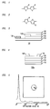
- FIG. 1 is an illustration of a regioregular homopolymer of 3-alkylthiophene monomers useful as the active semiconducting layer of a TFT.
- the alkyl group has at least two to twelve carbon atoms and is designated generally by the letter R in FIGs. 1 and 2.
- Examples of the alkyl groups include branched chains such as isopropyl and isobutyl as well as linear alkyl chains.
- the alkyl groups are either substituted or unsubstituted. If substituted, examples of suitable substituents include carboxylic acid, sulfonic acid, and thiol.
- FIG. 1 illustrates a structure in which the thiophene moieties are oriented uniformly with respect to the polymer backbone. Consequently, the R groups in FIG. 1 are on one side of the polymer chain.
- FIG. 2 illustrates a structure in which the orientation of the thiophene moieties in the chain with respect to the polymer backbone alternate between a first orientation and a second orientation.
- the R groups on the thiophene moieties with the first orientation are on a first side of the polymer backbone.
- R groups on the thiophene moieties with the second orientation are on the side of the polymer backbone opposite the first side. Since the location of the R groups in the polymers depicted in FIGs. 1 and 2 is regular, the structures are denominated as regioregular.
- Such a regioregular orientation of the R groups on the thiophene moieties that make up the polymer backbone will hereinafter be referred to as having a head-to-tail (HT) linkage.
- HT head-to-tail
- a homopolymer of 3-alkylthiophene monomers has at least 95 % HT linkages, with a small number of the thiophene moieties (less than about 5 %) in the polymer chain having an orientation that does not conform to the regioregular orientation.
- FIG. 3 illustrates an example of a metal-insulator-semiconductor (MIS) FET type device made using the process of the present invention.
- the MISFET 100 includes a substrate 110 over which a layer of insulating material 120 and a metal contact 130 are formed. Two additional metal contacts, 140 and 150 , are formed over the layer of insulating material. A layer of organic semiconducting material 160 is formed over and between the contacts 140 and 150 . (In another example of a MISFET, shown in FIG. 4, metal contact 130 is formed between the substrate 110 and the layer of insulating material 120 , and the metal contacts 140, 150 are formed on organic semiconducting material 160 ).
- the substrate 110 is made of conventional materials such as silicon, glass, or plastic.
- the contacts 130, 140, 150 are made of a conventional material for this purpose such as gold, indium-tin-oxide (ITO), conductive ink, or conducting polymer.
- ITO indium-tin-oxide
- the contacts 130, 140, 150 are formed using well known, conventional techniques which are not discussed in detail herein.
- the layer of insulating material 120 is an organic material.
- organic insulating materials include polyimides, polyesters, and polymethylmethacrylate (PMMA).
- the layer of insulating material is formed by casting, spin coating or printing the organic insulating material on the substrate surface.
- the insulating layer is printed on the substrate using a screen mask.
- the screen mask is made of a stainless steel fabric with 400 mesh count per inch and an emulsion thickness of about 7.5 micrometers ( ⁇ m).
- the organic material is applied to the stainless steel fabric and a squeegee (doctor blade) is used to press the organic material through the openings in the screen and onto the substrate surface.
- Insulating layers formed using such screen printing have thicknesses approximating 0.1 micrometers ( ⁇ m) to 1.0 micrometers ( ⁇ m). Typically, the capacitance of the insulating material should be about 10 -8 F/cm 2 (farads/square centimeter).
- the layer of insulating material is optionally formed of an inorganic material such as silicon dioxide, silicon nitride (Si 3 N 4 ), or aluminum oxide (Al 2 O 3 ), using well known conventional techniques.
- the active organic semiconducting material 160 is formed by applying a solution of the regioregular organic polymer and an appropriate solvent, using conventional techniques such as spin-coating, casting, or printing.
- regioregular poly (3-alkylthiophene) compounds are soluble in chlorinated organic solvents such as chloroform, methylene chloride, chlorobenzene, and tetrachloroethylene. It is desirable for the organic polymer to be completely dissolved in the solvent because discontinuities occur in films formed from solutions containing precipitated polymers.
- the thickness of the organic semiconducting material 160 is at least 300 ⁇ .
- MIS-FET type TFTs such as the MIS-FET shown in FIG. 3, are formed with a 12 ⁇ m channel length and a 250 ⁇ m gate length on an n-doped silicon substrate 110 .
- a 3000 ⁇ thick layer of silicon dioxide (SiO 2 ) is formed over the substrate 110 .
- the insulating material 120 is the SiO 2 layer having a capacitance of about 10 nF/cm 2 (nanofarads/square centimeter).
- a third contact is formed directly on the silicon substrate 110 .
- a layer of poly (3-alkylthiophene) is formed over the insulating material 120 and the contacts 140, 150 formed thereon.
- PTFE polytetraflouroethylene
- Devices were formed using the above identified regioregular poly (3-alkylthiophene) compounds as the active layer, as generally described above with reference to FIG. 3.
- the solution containing the dissolved polymer was applied over the insulating layer by casting, with the thickness of the resulting films dependent on the solution concentration.
- the substrate was dried in a vacuum environment for up to 24 hours.
- the poly (3-alkylthiophene) films were optionally exposed to gaseous ammonia (NH 3 ) for up to 10 hours, by placing the substrate in an enclosure where nitrogen (N 2 ) gas was bubbled through an ammonium hydroxide aqueous solution.
- NH 3 gaseous ammonia
- the range of values for the carrier mobility, conductivity, and on/off ratio reported in Table I were measured from devices formed using at least two substrates for each semiconducting material layer.
- semiconducting organic polymer layers with the hexyl substituents were formed on ten substrates with at least twenty devices formed on each substrate.
- the I DS at the saturated region is determined by observing the relationship between the drain-source voltage (V DS ) and the drain-source current at a given V G .
- I DS at the saturated region is where I DS no longer increases with increasing drain-source voltage.
- I DS at the saturated region varies with V G . This method for determining V 0 is conventional and well known to persons skilled in the art.
- FIG. 5 illustrates a very strong, sharp first order diffraction peak at 5.4°, a second order diffraction peak at 10.8°, and a third order diffraction peak at 16.3° corresponding to an intermolecular spacing of 16.36 ⁇ (see graph).
- Such an intermolecular spacing provides for the planar stacking (parallel to the substrate surface) of layers of thiophene chains, spaced apart by the alkyl groups.
- the thiophene polymer backbone is generally parallel to the substrate surface.
- Electron diffraction analysis performed for the same regioregular poly (3-hexylthiophene) films is also shown in the photograph of FIG. 5.
- Electron diffraction illustrates a major peak at about 3.7 - 3.8 ⁇ , which corresponds to the distance between the stacked thiophene rings in adjacent chains.
- Such a value for the thiophene ring spacing indicates a preferred orientation in which the hexyl groups are orientated about normal to the surface of the substrate with the direction of the stacked thiophene chains parallel to the substrate.
Landscapes
- Engineering & Computer Science (AREA)
- Chemical & Material Sciences (AREA)
- Materials Engineering (AREA)
- Manufacturing & Machinery (AREA)
- Thin Film Transistor (AREA)
- Electroluminescent Light Sources (AREA)
Applications Claiming Priority (2)
| Application Number | Priority Date | Filing Date | Title |
|---|---|---|---|
| US770535 | 1985-08-28 | ||
| US08/770,535 US6107117A (en) | 1996-12-20 | 1996-12-20 | Method of making an organic thin film transistor |
Publications (1)
| Publication Number | Publication Date |
|---|---|
| EP0852403A1 true EP0852403A1 (de) | 1998-07-08 |
Family
ID=25088888
Family Applications (1)
| Application Number | Title | Priority Date | Filing Date |
|---|---|---|---|
| EP97309718A Withdrawn EP0852403A1 (de) | 1996-12-20 | 1997-12-02 | Methode zur Herstellung eines organischen Dünnfilmtransistors |
Country Status (5)
| Country | Link |
|---|---|
| US (1) | US6107117A (de) |
| EP (1) | EP0852403A1 (de) |
| JP (1) | JPH10190001A (de) |
| KR (1) | KR19980064344A (de) |
| TW (1) | TW395059B (de) |
Cited By (22)
| Publication number | Priority date | Publication date | Assignee | Title |
|---|---|---|---|---|
| WO2000065653A1 (en) * | 1999-04-22 | 2000-11-02 | Thin Film Electronics Asa | A method in the fabrication of organic thin-film semiconducting devices |
| US6312971B1 (en) | 1999-08-31 | 2001-11-06 | E Ink Corporation | Solvent annealing process for forming a thin semiconductor film with advantageous properties |
| US6473072B1 (en) | 1998-05-12 | 2002-10-29 | E Ink Corporation | Microencapsulated electrophoretic electrostatically-addressed media for drawing device applications |
| US6498114B1 (en) | 1999-04-09 | 2002-12-24 | E Ink Corporation | Method for forming a patterned semiconductor film |
| US6518949B2 (en) | 1998-04-10 | 2003-02-11 | E Ink Corporation | Electronic displays using organic-based field effect transistors |
| US6545291B1 (en) | 1999-08-31 | 2003-04-08 | E Ink Corporation | Transistor design for use in the construction of an electronically driven display |
| EP1327646A1 (de) * | 2002-01-11 | 2003-07-16 | Xerox Corporation | Polythiophene und damit hergestellte Vorrichtungen |
| EP1327647A1 (de) * | 2002-01-11 | 2003-07-16 | Xerox Corporation | Polythiophene und damit hergestellte Vorrichtungen |
| EP1329475A1 (de) * | 2002-01-11 | 2003-07-23 | Xerox Corporation | Polythiophene und damit hergestellte Vorrichtungen |
| US6839158B2 (en) | 1997-08-28 | 2005-01-04 | E Ink Corporation | Encapsulated electrophoretic displays having a monolayer of capsules and materials and methods for making the same |
| US6842657B1 (en) | 1999-04-09 | 2005-01-11 | E Ink Corporation | Reactive formation of dielectric layers and protection of organic layers in organic semiconductor device fabrication |
| EP1439173A3 (de) * | 2002-10-18 | 2005-09-14 | H.C. Starck GmbH | Verfahren zur Herstellung linearer organischer Oligomere |
| US7250625B2 (en) | 2002-01-11 | 2007-07-31 | Xerox Corporation | Polythiophenes and electronic devices generated therefrom |
| US7297621B2 (en) | 2003-04-15 | 2007-11-20 | California Institute Of Technology | Flexible carbon-based ohmic contacts for organic transistors |
| EP1316116B1 (de) * | 2000-09-01 | 2009-07-22 | PolyIC GmbH & Co. KG | Verfahren zur strukturierung eines organischen feldeffekttransistors |
| US8022401B2 (en) | 2006-11-14 | 2011-09-20 | Idemitsu Kosan, Co., Ltd. | Organic thin film transistor and organic thin film light-emitting transistor |
| US8148720B2 (en) | 2006-11-24 | 2012-04-03 | Idemitsu Kosan Co., Ltd. | Organic thin film transistor and organic thin film light-emitting transistor |
| US8203139B2 (en) | 2006-11-24 | 2012-06-19 | Idemitsu Kosan Co., Ltd | Organic thin film transistor and organic thin film light-emitting transistor using an organic semiconductor layer having an aromatic hydrocarbon group or an aromatic heterocyclic group in the center thereof |
| EP1890346A3 (de) * | 1999-06-21 | 2012-06-20 | Cambridge Enterprise Limited | Ausgerichtete Polymere für einen organischen Dünnschichttransistor |
| US8217389B2 (en) | 2006-10-12 | 2012-07-10 | Idemitsu Kosan, Co., Ltd. | Organic thin film transistor device and organic thin film light-emitting transistor |
| CN101255156B (zh) * | 2007-01-24 | 2013-04-03 | 三星电子株式会社 | 含噻唑环合成物、聚合物、有源层、晶体管、器件及制法 |
| US8541257B2 (en) | 1999-06-21 | 2013-09-24 | Cambridge University Technical Services Limited | Aligned polymers for an organic TFT |
Families Citing this family (167)
| Publication number | Priority date | Publication date | Assignee | Title |
|---|---|---|---|---|
| US7075502B1 (en) | 1998-04-10 | 2006-07-11 | E Ink Corporation | Full color reflective display with multichromatic sub-pixels |
| US6335539B1 (en) | 1999-11-05 | 2002-01-01 | International Business Machines Corporation | Method for improving performance of organic semiconductors in bottom electrode structure |
| US6429040B1 (en) * | 2000-04-06 | 2002-08-06 | Agere Systems Guardian Corp. | Device comprising a bipolar semi-conducting film |
| US6414164B1 (en) * | 2000-07-12 | 2002-07-02 | International Business Machines Corporation | Synthesis of soluble derivatives of sexithiophene and their use as the semiconducting channels in thin-film filed-effect transistors |
| DE10034873B4 (de) * | 2000-07-18 | 2005-10-13 | Pacifica Group Technologies Pty Ltd | Verfahren und Bremsanlage zum Regeln des Bremsvorgangs bei einem Kraftfahrzeug |
| GB0028867D0 (en) | 2000-11-28 | 2001-01-10 | Avecia Ltd | Field effect translators,methods for the manufacture thereof and materials therefor |
| JP3856202B2 (ja) | 2001-10-05 | 2006-12-13 | 日本電気株式会社 | 有機薄膜トランジスタ |
| JP3963693B2 (ja) * | 2001-10-15 | 2007-08-22 | 富士通株式会社 | 導電性有機化合物及び電子素子 |
| JP3823312B2 (ja) | 2001-10-18 | 2006-09-20 | 日本電気株式会社 | 有機薄膜トランジスタ |
| US6602974B1 (en) * | 2001-12-04 | 2003-08-05 | Carnegie Mellon University | Polythiophenes, block copolymers made therefrom, and methods of forming the same |
| JP4247377B2 (ja) * | 2001-12-28 | 2009-04-02 | 独立行政法人産業技術総合研究所 | 薄膜トランジスタ及びその製造方法 |
| US7141644B2 (en) | 2002-01-11 | 2006-11-28 | Xerox Corporation | Polthiophenes and devices thereof |
| US6777529B2 (en) | 2002-01-11 | 2004-08-17 | Xerox Corporation | Polythiophenes and devices thereof |
| US6621099B2 (en) * | 2002-01-11 | 2003-09-16 | Xerox Corporation | Polythiophenes and devices thereof |
| WO2003067667A1 (en) * | 2002-02-08 | 2003-08-14 | Dai Nippon Printing Co., Ltd. | Organic semiconductor structure, process for producing the same, and organic semiconductor device |
| WO2003080730A1 (en) | 2002-03-20 | 2003-10-02 | Michigan Biotechnology Institute | Conductive polymer-based material |
| WO2003089515A1 (en) * | 2002-04-22 | 2003-10-30 | Konica Minolta Holdings, Inc. | Organic semiconductor composition, organic semiconductor element, and process for producing the same |
| US20030227014A1 (en) * | 2002-06-11 | 2003-12-11 | Xerox Corporation. | Process for forming semiconductor layer of micro-and nano-electronic devices |
| DE10228772A1 (de) * | 2002-06-27 | 2004-01-15 | Infineon Technologies Ag | Verringerung des Kontaktwiderstandes in organischen Feldeffekttransistoren mit Palladiumkontakten durch Verwendung von Nitrilen und Isonitrilen |
| US7078702B2 (en) * | 2002-07-25 | 2006-07-18 | General Electric Company | Imager |
| JP2004095874A (ja) * | 2002-08-30 | 2004-03-25 | Pioneer Electronic Corp | 有機半導体素子及びその製造方法 |
| KR100524552B1 (ko) * | 2002-09-28 | 2005-10-28 | 삼성전자주식회사 | 유기 게이트 절연막 및 이를 이용한 유기박막 트랜지스터 |
| US6803262B2 (en) * | 2002-10-17 | 2004-10-12 | Xerox Corporation | Process using self-organizable polymer |
| US6890868B2 (en) * | 2002-10-17 | 2005-05-10 | Xerox Corporation | Process for depositing gelable composition that includes dissolving gelable composition in liquid with agitating to disrupt gelling |
| US20040119049A1 (en) * | 2002-12-04 | 2004-06-24 | Martin Heeney | Mono-, oligo- and poly-bis(thienyl) arylenes and their use as charge transport materials |
| JP4892973B2 (ja) | 2003-02-18 | 2012-03-07 | コニカミノルタホールディングス株式会社 | 有機薄膜トランジスタ素子の製造方法 |
| US6855951B2 (en) | 2003-03-19 | 2005-02-15 | Xerox Corporation | Fluorinated polythiophenes and devices thereof |
| US6960643B2 (en) * | 2003-03-19 | 2005-11-01 | Xerox Corporation | Fluorinated polythiophenes and devices thereof |
| US6897284B2 (en) * | 2003-03-19 | 2005-05-24 | Xerox Corporation | Polythiophenes and devices thereof |
| JP4366116B2 (ja) * | 2003-05-20 | 2009-11-18 | キヤノン株式会社 | 電界効果型有機トランジスタ |
| JP4470398B2 (ja) * | 2003-06-23 | 2010-06-02 | Tdk株式会社 | 電界効果トランジスタ |
| CN100490205C (zh) * | 2003-07-10 | 2009-05-20 | 国际商业机器公司 | 淀积金属硫族化物膜的方法和制备场效应晶体管的方法 |
| JP4194436B2 (ja) * | 2003-07-14 | 2008-12-10 | キヤノン株式会社 | 電界効果型有機トランジスタ |
| US7049629B2 (en) * | 2003-08-22 | 2006-05-23 | Xerox Corporation | Semiconductor polymers and devices thereof |
| US7169883B2 (en) * | 2003-08-22 | 2007-01-30 | Xerox Corporation | Polymers |
| JPWO2005022660A1 (ja) * | 2003-08-29 | 2006-10-26 | 松下電器産業株式会社 | 有機半導体膜、それを用いた電子デバイス、およびそれらの製造方法 |
| JP4365825B2 (ja) * | 2003-11-11 | 2009-11-18 | パナソニック株式会社 | 薄膜トランジスタ及びその製造方法 |
| CN100428521C (zh) | 2003-11-17 | 2008-10-22 | 富士施乐株式会社 | 有机半导体晶体管元件 |
| KR101007787B1 (ko) * | 2003-12-08 | 2011-01-14 | 삼성전자주식회사 | 퀴녹살린환을 주쇄에 포함하는 유기박막 트랜지스터용유기반도체 고분자 |
| WO2005089450A2 (en) * | 2004-03-19 | 2005-09-29 | Ohio University | Organic semiconductor devices and methods |
| JP4449549B2 (ja) | 2004-04-15 | 2010-04-14 | 日本電気株式会社 | 有橋環式炭化水素ラクトン構造を有する材料を用いた有機薄膜トランジスタとその製造方法 |
| US7312469B2 (en) * | 2004-06-10 | 2007-12-25 | Xerox Corporation | Device with small molecular thiophene compound |
| JP4731840B2 (ja) * | 2004-06-14 | 2011-07-27 | キヤノン株式会社 | 電界効果型トランジスタおよびその製造方法 |
| US7476599B2 (en) * | 2004-06-22 | 2009-01-13 | Changchun Institute Of Applied Chemistry | Two-phase thermal method for preparation of cadmium sulfide quantum dots |
| US7300861B2 (en) * | 2004-06-24 | 2007-11-27 | Palo Alto Research Center Incorporated | Method for interconnecting electronic components using a blend solution to form a conducting layer and an insulating layer |
| US7351606B2 (en) * | 2004-06-24 | 2008-04-01 | Palo Alto Research Center Incorporated | Method for forming a bottom gate thin film transistor using a blend solution to form a semiconducting layer and an insulating layer |
| KR101069519B1 (ko) | 2004-07-08 | 2011-09-30 | 삼성전자주식회사 | 올리고티오펜과 n-형 방향족 화합물을 주쇄에 교호로 포함하는 유기 반도체 고분자 |
| KR101001441B1 (ko) * | 2004-08-17 | 2010-12-14 | 삼성전자주식회사 | 유무기 금속 하이브리드 물질 및 이를 포함하는 유기절연체 조성물 |
| EP1737027B1 (de) * | 2004-08-20 | 2017-10-11 | Panasonic Intellectual Property Management Co., Ltd. | Beschichtungsflüssigkeit zum formen von organischen mehrschichtfolien, verfahren zur herstellung eines feldeffekttransistors und feldeffekttransistor |
| WO2006038459A1 (ja) * | 2004-10-01 | 2006-04-13 | Konica Minolta Holdings, Inc. | 有機薄膜トランジスタ材料、有機薄膜トランジスタ、電界効果トランジスタ及びスイッチング素子 |
| US7270694B2 (en) | 2004-10-05 | 2007-09-18 | Xerox Corporation | Stabilized silver nanoparticles and their use |
| KR101224708B1 (ko) * | 2004-10-19 | 2013-01-21 | 삼성전자주식회사 | (올리고티오펜-아릴렌) 유도체 및 이를 이용한유기박막트랜지스터 |
| US7355199B2 (en) * | 2004-11-02 | 2008-04-08 | E.I. Du Pont De Nemours And Company | Substituted anthracenes and electronic devices containing the substituted anthracenes |
| KR101151082B1 (ko) * | 2004-11-29 | 2012-06-01 | 삼성전자주식회사 | 스타형 (올리고티오펜-아릴렌) 유도체 및 이를 이용한유기박막 트랜지스터 |
| KR20060081441A (ko) * | 2005-01-07 | 2006-07-13 | 삼성전자주식회사 | 신규한 티오펜-티아졸 유도체 및 이를 이용한 유기박막트랜지스터 |
| JP2006219550A (ja) * | 2005-02-09 | 2006-08-24 | Konica Minolta Holdings Inc | 有機半導体材料、有機薄膜トランジスタ、電界効果トランジスタ及びスイッチング素子 |
| KR101314877B1 (ko) * | 2005-02-10 | 2013-10-04 | 플렉스트로닉스, 인크 | 정공 주입/수송 층 조성물 및 장치 |
| JP2006232986A (ja) * | 2005-02-24 | 2006-09-07 | Mitsubishi Chemicals Corp | 導電性高分子並びにそれを用いた有機電子デバイス及び電界効果トランジスタ |
| US7619242B2 (en) * | 2005-02-25 | 2009-11-17 | Xerox Corporation | Celluloses and devices thereof |
| US7598518B2 (en) | 2005-03-07 | 2009-10-06 | Ricoh Company, Ltd. | Organic transistor with light emission, organic transistor unit and display device incorporating the organic transistor |
| US7321021B2 (en) * | 2005-03-22 | 2008-01-22 | Xerox Corporation | Removing impurities from polythiophene |
| US8089062B2 (en) * | 2005-03-23 | 2012-01-03 | Xerox Corporation | Wax encapsulated electronic devices |
| US7511296B2 (en) | 2005-03-25 | 2009-03-31 | Canon Kabushiki Kaisha | Organic semiconductor device, field-effect transistor, and their manufacturing methods |
| KR101102158B1 (ko) | 2005-05-11 | 2012-01-02 | 삼성전자주식회사 | 신규한 유기 고분자 반도체, 이를 이용한 유기 고분자반도체 박막의 형성방법 및 이를 이용한 유기박막트랜지스터 |
| JPWO2006137233A1 (ja) * | 2005-06-21 | 2009-01-08 | コニカミノルタホールディングス株式会社 | 有機半導体材料薄膜の形成方法および有機薄膜トランジスタの製造方法 |
| KR101139038B1 (ko) * | 2005-06-28 | 2012-05-02 | 삼성전자주식회사 | 피리미도피리미딘 유도체 및 이를 이용한 유기 박막 트랜지스터 |
| KR20080047543A (ko) | 2005-08-31 | 2008-05-29 | 스미또모 가가꾸 가부시끼가이샤 | 트랜지스터, 유기 반도체 소자, 및 이들의 제조 방법 |
| CN101253609B (zh) | 2005-08-31 | 2012-06-13 | 住友化学株式会社 | 晶体管及其制造方法、以及具有该晶体管的半导体装置 |
| JP2006093725A (ja) * | 2005-10-18 | 2006-04-06 | Matsushita Electric Ind Co Ltd | 電子デバイス |
| JP2007134629A (ja) | 2005-11-14 | 2007-05-31 | Konica Minolta Holdings Inc | 半導体層の成膜方法、半導体層を成膜する製造装置 |
| US8637138B2 (en) | 2005-12-27 | 2014-01-28 | Palo Alto Research Center Incorporated | Layered structures on thin substrates |
| US7816146B2 (en) * | 2005-12-27 | 2010-10-19 | Palo Alto Research Center Incorporated | Passive electronic devices |
| US7784173B2 (en) * | 2005-12-27 | 2010-08-31 | Palo Alto Research Center Incorporated | Producing layered structures using printing |
| JP5066848B2 (ja) | 2006-02-10 | 2012-11-07 | コニカミノルタホールディングス株式会社 | 薄膜トランジスタの製造方法 |
| US7521710B2 (en) | 2006-02-16 | 2009-04-21 | Idemitsu Kosan Co., Ltd. | Organic thin film transistor |
| US7640749B2 (en) * | 2006-02-16 | 2010-01-05 | Yousoufian Hrant H | Moisture separator and reheater |
| US7517477B2 (en) * | 2006-04-06 | 2009-04-14 | Xerox Corporation | Polydiazaacenes and electronic devices generated therefrom |
| US8334391B2 (en) * | 2006-04-06 | 2012-12-18 | Xerox Corporation | Functionalized heteroacenes |
| US7517476B2 (en) * | 2006-04-06 | 2009-04-14 | Xerox Corporation | Polydiazaacenes |
| US7847052B2 (en) * | 2006-04-06 | 2010-12-07 | Xerox Corporation | Linked arylamine polymers |
| US8049205B2 (en) * | 2006-04-06 | 2011-11-01 | Xerox Corporation | Poly(alkynylthiophene)s and electronic devices generated therefrom |
| US7550760B2 (en) * | 2006-04-06 | 2009-06-23 | Xerox Corporation | Polyacenes and electronic devices generated therefrom |
| US7563860B2 (en) * | 2006-04-06 | 2009-07-21 | Xerox Corporation | Semiconductors and electronic devices generated therefrom |
| US7557370B2 (en) * | 2006-04-06 | 2009-07-07 | Xerox Corporation | Heteroacene polymers and electronic devices generated therefrom |
| US7619055B2 (en) * | 2006-04-06 | 2009-11-17 | Xerox Corporation | Linked arylamine polymers and electronic devices generated therefrom |
| US7705111B2 (en) * | 2006-04-06 | 2010-04-27 | Xerox Corporation | Poly(alkynylthiophene)s |
| US7586120B2 (en) * | 2006-04-06 | 2009-09-08 | Xerox Corporation | Ethynylene acene polymers and electronic devices generated therefrom |
| US7372071B2 (en) * | 2006-04-06 | 2008-05-13 | Xerox Corporation | Functionalized heteroacenes and electronic devices generated therefrom |
| US7615607B2 (en) * | 2006-04-06 | 2009-11-10 | Xerox Corporation | Semiconductor polymers |
| US7449715B2 (en) * | 2006-04-06 | 2008-11-11 | Xerox Corporation | Poly[bis(ethynyl)heteroacene]s and electronic devices generated therefrom |
| US7795373B2 (en) * | 2006-04-06 | 2010-09-14 | Xerox Corporation | Ethynylene acene polymers |
| CN100555702C (zh) * | 2006-04-29 | 2009-10-28 | 中国科学院长春应用化学研究所 | 有机半导体晶体薄膜及弱取向外延生长制备方法和应用 |
| JP2007311677A (ja) | 2006-05-22 | 2007-11-29 | Konica Minolta Holdings Inc | 有機薄膜トランジスタの製造方法、有機薄膜トランジスタ |
| WO2007142238A1 (ja) * | 2006-06-07 | 2007-12-13 | Panasonic Corporation | 半導体素子およびその製造方法ならびに電子デバイスおよびその製造方法 |
| WO2008105816A2 (en) * | 2006-08-22 | 2008-09-04 | Northwestern University | Gate dielectric structures, organic semiconductors, thin film transistors and related methods |
| KR100737383B1 (ko) | 2006-09-11 | 2007-07-09 | 한국전자통신연구원 | 절연막, 이를 이용한 유기박막 트랜지스터 및 제조방법 |
| KR101314931B1 (ko) * | 2006-10-30 | 2013-10-04 | 삼성전자주식회사 | 유기 고분자 반도체, 이의 제조방법 및 이를 이용한 양극성 유기 박막 트랜지스터 |
| KR101249090B1 (ko) * | 2006-11-14 | 2013-03-29 | 삼성전자주식회사 | 유기 절연막 형성용 조성물, 이를 이용하여 제조된 유기절연막 |
| KR20090080522A (ko) | 2006-11-14 | 2009-07-24 | 이데미쓰 고산 가부시키가이샤 | 유기 박막 트랜지스터 및 유기 박막 발광 트랜지스터 |
| JPWO2008069061A1 (ja) * | 2006-12-04 | 2010-03-18 | 出光興産株式会社 | 有機薄膜トランジスタ及び有機薄膜発光トランジスタ |
| JP5308164B2 (ja) * | 2006-12-04 | 2013-10-09 | 出光興産株式会社 | 有機薄膜トランジスタ及び有機薄膜発光トランジスタ |
| US7718998B2 (en) | 2006-12-14 | 2010-05-18 | Xerox Corporation | Thiophene electronic devices |
| US7795614B2 (en) | 2007-04-02 | 2010-09-14 | Xerox Corporation | Device with phase-separated dielectric structure |
| US7754510B2 (en) | 2007-04-02 | 2010-07-13 | Xerox Corporation | Phase-separated dielectric structure fabrication process |
| JP2009021297A (ja) | 2007-07-10 | 2009-01-29 | Sumitomo Chemical Co Ltd | 有機半導体素子の製造方法、有機半導体素子及び有機半導体装置 |
| US7829375B2 (en) | 2007-07-18 | 2010-11-09 | Konica Minolta Holdings, Inc. | Method for manufacturing organic thin film transistor and organic thin film transistor |
| US7932344B2 (en) * | 2007-09-06 | 2011-04-26 | Xerox Corporation | Diketopyrrolopyrrole-based polymers |
| US7910684B2 (en) | 2007-09-06 | 2011-03-22 | Xerox Corporation | Diketopyrrolopyrrole-based derivatives for thin film transistors |
| EP2043061A1 (de) * | 2007-09-28 | 2009-04-01 | Innospense Capital B.V. | Abgabevorrichtung und Verfahren zur Abgabe einzelner Waren, insbesondere Medikamentenverpackungen |
| US20090111086A1 (en) * | 2007-10-18 | 2009-04-30 | Katz Howard E | Kit for facile deposition and evaluation of semiconductor devices |
| KR101377924B1 (ko) | 2007-11-08 | 2014-03-25 | 삼성전자주식회사 | 페닐렌 비닐렌-올리고아릴렌 비닐렌 교호공중합체, 이의제조방법 및 이를 포함하는 유기박막 트랜지스터 |
| KR101377842B1 (ko) * | 2007-11-08 | 2014-03-25 | 삼성전자주식회사 | 페닐렌 비닐렌-바이아릴렌 비닐렌 교호공중합체, 이의제조방법 및 이를 포함하는 유기박막 트랜지스터 |
| US20090142482A1 (en) * | 2007-11-30 | 2009-06-04 | Xerox Corporation | Methods of Printing Conductive Silver Features |
| US20090148600A1 (en) * | 2007-12-05 | 2009-06-11 | Xerox Corporation | Metal Nanoparticles Stabilized With a Carboxylic Acid-Organoamine Complex |
| DE602008001431D1 (de) | 2007-12-27 | 2010-07-15 | Ind Tech Res Inst | Lösliche Polythiophenderivate |
| KR101450137B1 (ko) * | 2008-01-25 | 2014-10-13 | 삼성전자주식회사 | 유기반도체용 공중합체 및 이를 이용한 유기박막트랜지스터 및 유기 전자소자 |
| US8329504B2 (en) * | 2008-02-12 | 2012-12-11 | Konica Minolta Holdings, Inc. | Method of forming organic semiconductor layer and method of manufacturing organic thin film transistor |
| US20090224011A1 (en) * | 2008-03-07 | 2009-09-10 | Sperbeck Bryanlee P | Method of and an apparatus for assisting in putting on and taking off a wet suit used by water enthusiasts |
| US8298314B2 (en) | 2008-08-18 | 2012-10-30 | Xerox Corporation | Silver nanoparticles and process for producing same |
| US7821068B2 (en) | 2008-08-18 | 2010-10-26 | Xerox Corporation | Device and process involving pinhole undercut area |
| US8419822B2 (en) | 2008-08-18 | 2013-04-16 | Xerox Corporation | Methods for producing carboxylic acid stabilized silver nanoparticles |
| US8834965B2 (en) | 2009-02-12 | 2014-09-16 | Xerox Corporation | Organoamine stabilized silver nanoparticles and process for producing same |
| JP5658174B2 (ja) * | 2009-03-04 | 2015-01-21 | ゼロックス コーポレイションXerox Corporation | 複合材構造化有機薄膜 |
| US7935278B2 (en) | 2009-03-05 | 2011-05-03 | Xerox Corporation | Feature forming process using acid-containing composition |
| US20100233361A1 (en) * | 2009-03-12 | 2010-09-16 | Xerox Corporation | Metal nanoparticle composition with improved adhesion |
| JP2010225758A (ja) * | 2009-03-23 | 2010-10-07 | Fuji Xerox Co Ltd | 有機半導体トランジスタ |
| JP4893767B2 (ja) * | 2009-03-24 | 2012-03-07 | 富士ゼロックス株式会社 | 有機半導体トランジスタ |
| JP5347690B2 (ja) * | 2009-04-30 | 2013-11-20 | 富士ゼロックス株式会社 | 有機電界発光素子、及び表示媒体 |
| TWI418571B (zh) * | 2009-05-15 | 2013-12-11 | 財團法人工業技術研究院 | 可溶性聚噻吩衍生物 |
| US8164089B2 (en) * | 2009-10-08 | 2012-04-24 | Xerox Corporation | Electronic device |
| US8366971B2 (en) | 2010-04-02 | 2013-02-05 | Xerox Corporation | Additive for robust metal ink formulations |
| JP5701861B2 (ja) | 2010-04-22 | 2015-04-15 | 出光興産株式会社 | 有機薄膜トランジスタ |
| US9076975B2 (en) | 2010-04-27 | 2015-07-07 | Xerox Corporation | Dielectric composition for thin-film transistors |
| US8765025B2 (en) | 2010-06-09 | 2014-07-01 | Xerox Corporation | Silver nanoparticle composition comprising solvents with specific hansen solubility parameters |
| US8147908B2 (en) | 2010-06-09 | 2012-04-03 | Xerox Corporation | Increased throughput for large-scale production of low melt organoamine stabilized silver nano-particles |
| US9567425B2 (en) | 2010-06-15 | 2017-02-14 | Xerox Corporation | Periodic structured organic films |
| US8318892B2 (en) | 2010-07-28 | 2012-11-27 | Xerox Corporation | Capped structured organic film compositions |
| US8697322B2 (en) | 2010-07-28 | 2014-04-15 | Xerox Corporation | Imaging members comprising structured organic films |
| US8257889B2 (en) | 2010-07-28 | 2012-09-04 | Xerox Corporation | Imaging members comprising capped structured organic film compositions |
| US8119315B1 (en) | 2010-08-12 | 2012-02-21 | Xerox Corporation | Imaging members for ink-based digital printing comprising structured organic films |
| US8119314B1 (en) | 2010-08-12 | 2012-02-21 | Xerox Corporation | Imaging devices comprising structured organic films |
| US8158032B2 (en) | 2010-08-20 | 2012-04-17 | Xerox Corporation | Silver nanoparticle ink composition for highly conductive features with enhanced mechanical properties |
| US8623447B2 (en) | 2010-12-01 | 2014-01-07 | Xerox Corporation | Method for coating dielectric composition for fabricating thin-film transistors |
| US8759473B2 (en) | 2011-03-08 | 2014-06-24 | Xerox Corporation | High mobility periodic structured organic films |
| US8586134B2 (en) | 2011-05-06 | 2013-11-19 | Xerox Corporation | Method of fabricating high-resolution features |
| US20120288697A1 (en) * | 2011-05-13 | 2012-11-15 | Xerox Corporation | Coating methods using silver nanoparticles |
| US8353574B1 (en) | 2011-06-30 | 2013-01-15 | Xerox Corporation | Ink jet faceplate coatings comprising structured organic films |
| US8247142B1 (en) | 2011-06-30 | 2012-08-21 | Xerox Corporation | Fluorinated structured organic film compositions |
| US8377999B2 (en) | 2011-07-13 | 2013-02-19 | Xerox Corporation | Porous structured organic film compositions |
| US8313560B1 (en) | 2011-07-13 | 2012-11-20 | Xerox Corporation | Application of porous structured organic films for gas separation |
| US8410016B2 (en) | 2011-07-13 | 2013-04-02 | Xerox Corporation | Application of porous structured organic films for gas storage |
| US20130029034A1 (en) | 2011-07-28 | 2013-01-31 | Xerox Corporation | Process for producing silver nanoparticles |
| US8372566B1 (en) | 2011-09-27 | 2013-02-12 | Xerox Corporation | Fluorinated structured organic film photoreceptor layers |
| US8460844B2 (en) | 2011-09-27 | 2013-06-11 | Xerox Corporation | Robust photoreceptor surface layer |
| JP5966353B2 (ja) | 2011-12-26 | 2016-08-10 | 富士ゼロックス株式会社 | 有機半導体トランジスタ |
| US8529997B2 (en) | 2012-01-17 | 2013-09-10 | Xerox Corporation | Methods for preparing structured organic film micro-features by inkjet printing |
| US8558109B2 (en) | 2012-03-19 | 2013-10-15 | Xerox Corporation | Semiconductor composition for high performance organic devices |
| US8563851B2 (en) | 2012-03-19 | 2013-10-22 | Xerox Corporation | Method to increase field effect mobility of donor-acceptor semiconductors |
| US8765340B2 (en) | 2012-08-10 | 2014-07-01 | Xerox Corporation | Fluorinated structured organic film photoreceptor layers containing fluorinated secondary components |
| KR101461136B1 (ko) * | 2012-10-18 | 2014-11-13 | 광주과학기술원 | 세미플루오로 알킬기가 치환된 유기 반도체 고분자 및 이를 포함하는 유기 박막 트랜지스터 |
| US8575477B1 (en) | 2012-12-27 | 2013-11-05 | Xerox Corporation | Diketopyrrolopyrrole-based polymers containing a diene group for semiconductors |
| US8906462B2 (en) | 2013-03-14 | 2014-12-09 | Xerox Corporation | Melt formulation process for preparing structured organic films |
| KR20160082287A (ko) | 2014-12-30 | 2016-07-08 | 도레이케미칼 주식회사 | 플렉서블 oled소자의 기재용 평탄화 필름 및 이를 포함하는 플렉서블 oled소자 |
| KR20160082344A (ko) | 2014-12-30 | 2016-07-08 | 도레이케미칼 주식회사 | 플렉서블 oled소자 및 이의 제조방법 |
| TWI692002B (zh) * | 2017-02-28 | 2020-04-21 | 財團法人國家實驗研究院 | 可撓式基板結構、可撓式電晶體及其製造方法 |
| CN111032567B (zh) | 2017-08-31 | 2023-05-09 | 松下知识产权经营株式会社 | 杂富勒烯以及使用了其的n型半导体膜和电子设备 |
| CN111052429B (zh) | 2017-08-31 | 2023-07-04 | 松下知识产权经营株式会社 | 包含杂富勒烯的p型半导体膜和电子设备 |
Citations (1)
| Publication number | Priority date | Publication date | Assignee | Title |
|---|---|---|---|---|
| WO1992001313A1 (fr) * | 1990-07-04 | 1992-01-23 | Centre National De La Recherche Scientifique (Cnrs) | Transistors a effet de champ en couche mince de structure mis, dont l'isolant et le semiconducteur sont realises en materiaux organiques |
Family Cites Families (3)
| Publication number | Priority date | Publication date | Assignee | Title |
|---|---|---|---|---|
| US5498761A (en) * | 1988-10-11 | 1996-03-12 | Wessling; Bernhard | Process for producing thin layers of conductive polymers |
| US5574291A (en) * | 1994-12-09 | 1996-11-12 | Lucent Technologies Inc. | Article comprising a thin film transistor with low conductivity organic layer |
| TW293172B (de) * | 1994-12-09 | 1996-12-11 | At & T Corp |
-
1996
- 1996-12-20 US US08/770,535 patent/US6107117A/en not_active Expired - Lifetime
-
1997
- 1997-12-02 JP JP9331398A patent/JPH10190001A/ja active Pending
- 1997-12-02 EP EP97309718A patent/EP0852403A1/de not_active Withdrawn
- 1997-12-10 TW TW086118596A patent/TW395059B/zh not_active IP Right Cessation
- 1997-12-19 KR KR1019970070572A patent/KR19980064344A/ko not_active Withdrawn
Patent Citations (1)
| Publication number | Priority date | Publication date | Assignee | Title |
|---|---|---|---|---|
| WO1992001313A1 (fr) * | 1990-07-04 | 1992-01-23 | Centre National De La Recherche Scientifique (Cnrs) | Transistors a effet de champ en couche mince de structure mis, dont l'isolant et le semiconducteur sont realises en materiaux organiques |
Non-Patent Citations (8)
| Title |
|---|
| CHEN F ET AL: "IMPROVED ELECTROLUMINESCENCE PERFORMANCE OF POLY 3-(ALKYLTHIOPHENES) HAVING A HIGH HEAD-TO-TAIL (HT) RATIO", JOURNAL OF MATERIALS CHEMISTRY, vol. 6, no. 11, November 1996 (1996-11-01), pages 1763 - 1766, XP000633857 * |
| DIMITRAKOPOULOS C D ET AL: "trans-trans-2,5-bis- 2-{5-2,2'-bithienyl}ethenylthiophene: synthesis, characterization, thin film deposition and fabrication of organic field-effect transistors", SYNTHETIC METALS, SEPT. 1997, ELSEVIER, SWITZERLAND, vol. 89, no. 3, ISSN 0379-6779, pages 193 - 197, XP002059691 * |
| FUCHIGAMI H ET AL: "Polythienylenevinylene thin-film transistor with high carrier mobility", APPLIED PHYSICS LETTERS, 6 SEPT. 1993, USA, vol. 63, no. 10, ISSN 0003-6951, pages 1372 - 1374, XP000394584 * |
| HIROYUKI FUCHIGAMI ET AL: "A NEW TYPE OF TFT BASED ON A POLYMERIC SEMICONDUCTOR", JAPANESE JOURNAL OF APPLIED PHYSICS, SUPPLEMENTS, 27 August 1991 (1991-08-27), pages 596 - 598, XP000279503 * |
| HOROWITZ G ET AL: "Structure dependent properties of organic field-effect transistors", 9TH EUROPEAN HYBRID MICROELECTRONIC CONFERENCE PROCEEDINGS, PROCEEDINGS OF 9TH ISHM-EUROPEAN HYBRID MICROELECTRONICS CONFERENCE, NICE, FRANCE, 2-4 JUNE 1993, 1993, VERSAILLES, FRANCE, INT. SOC. HYBRID MICROELECTRON, FRANCE, pages 60 - 67, XP002059692 * |
| XUEZHOU PENG ET AL: "ALL-ORGANIC THIN-FILM TRANSISTORS MADE OF ALPHA-SEXITHIENYL SEMICONDUCTING AND VARIOUS POLYMERIC INSULATING LAYERS", APPLIED PHYSICS LETTERS, vol. 57, no. 19, 5 November 1990 (1990-11-05), pages 2013 - 2015, XP000172667 * |
| YUTAKA OHMORI ET AL: "FABRICATION AND CHARACTERISTICS OF SCHOTTKY GATED POLY (3-ALKYLTHIOPHENE) FIELD EFFECT TRANSISTORS", JAPANESE JOURNAL OF APPLIED PHYSICS, vol. 30, no. 4A, 1 April 1991 (1991-04-01), pages L610 - L611, XP000225828 * |
| ZHENAN BAO ET AL: "Soluble and processable regioregular poly(3-hexylthiophene) for thin film field-effect transistor applications with high mobility", APPLIED PHYSICS LETTERS, 23 DEC. 1996, AIP, USA, vol. 69, no. 26, ISSN 0003-6951, pages 4108 - 4110, XP002059693 * |
Cited By (36)
| Publication number | Priority date | Publication date | Assignee | Title |
|---|---|---|---|---|
| US6839158B2 (en) | 1997-08-28 | 2005-01-04 | E Ink Corporation | Encapsulated electrophoretic displays having a monolayer of capsules and materials and methods for making the same |
| US6518949B2 (en) | 1998-04-10 | 2003-02-11 | E Ink Corporation | Electronic displays using organic-based field effect transistors |
| US6473072B1 (en) | 1998-05-12 | 2002-10-29 | E Ink Corporation | Microencapsulated electrophoretic electrostatically-addressed media for drawing device applications |
| US6738050B2 (en) | 1998-05-12 | 2004-05-18 | E Ink Corporation | Microencapsulated electrophoretic electrostatically addressed media for drawing device applications |
| US6498114B1 (en) | 1999-04-09 | 2002-12-24 | E Ink Corporation | Method for forming a patterned semiconductor film |
| US6842657B1 (en) | 1999-04-09 | 2005-01-11 | E Ink Corporation | Reactive formation of dielectric layers and protection of organic layers in organic semiconductor device fabrication |
| US6852555B1 (en) | 1999-04-22 | 2005-02-08 | Thin Film Electronics Asa | Method in the fabrication of organic thin-film semiconducting devices |
| WO2000065653A1 (en) * | 1999-04-22 | 2000-11-02 | Thin Film Electronics Asa | A method in the fabrication of organic thin-film semiconducting devices |
| US8541257B2 (en) | 1999-06-21 | 2013-09-24 | Cambridge University Technical Services Limited | Aligned polymers for an organic TFT |
| EP1890346A3 (de) * | 1999-06-21 | 2012-06-20 | Cambridge Enterprise Limited | Ausgerichtete Polymere für einen organischen Dünnschichttransistor |
| US6545291B1 (en) | 1999-08-31 | 2003-04-08 | E Ink Corporation | Transistor design for use in the construction of an electronically driven display |
| US6750473B2 (en) | 1999-08-31 | 2004-06-15 | E-Ink Corporation | Transistor design for use in the construction of an electronically driven display |
| US6312971B1 (en) | 1999-08-31 | 2001-11-06 | E Ink Corporation | Solvent annealing process for forming a thin semiconductor film with advantageous properties |
| EP1316116B1 (de) * | 2000-09-01 | 2009-07-22 | PolyIC GmbH & Co. KG | Verfahren zur strukturierung eines organischen feldeffekttransistors |
| US7132682B2 (en) | 2002-01-11 | 2006-11-07 | Xerox Corporation | Polythiophenes and devices thereof |
| US7781564B2 (en) | 2002-01-11 | 2010-08-24 | Xerox Corporation | Polythiophenes and devices thereof |
| EP1327646A1 (de) * | 2002-01-11 | 2003-07-16 | Xerox Corporation | Polythiophene und damit hergestellte Vorrichtungen |
| US6949762B2 (en) | 2002-01-11 | 2005-09-27 | Xerox Corporation | Polythiophenes and devices thereof |
| US6770904B2 (en) | 2002-01-11 | 2004-08-03 | Xerox Corporation | Polythiophenes and electronic devices generated therefrom |
| US7132500B2 (en) * | 2002-01-11 | 2006-11-07 | Xerox Corporation | Polythiophenes and devices thereof |
| US7250625B2 (en) | 2002-01-11 | 2007-07-31 | Xerox Corporation | Polythiophenes and electronic devices generated therefrom |
| US7256418B2 (en) | 2002-01-11 | 2007-08-14 | Xerox Corporation | Polythiophenes and devices thereof |
| EP1327647A1 (de) * | 2002-01-11 | 2003-07-16 | Xerox Corporation | Polythiophene und damit hergestellte Vorrichtungen |
| EP1329475A1 (de) * | 2002-01-11 | 2003-07-23 | Xerox Corporation | Polythiophene und damit hergestellte Vorrichtungen |
| US7767999B2 (en) | 2002-01-11 | 2010-08-03 | Xerox Corporation | Polythiophenes and devices thereof |
| US6872801B2 (en) | 2002-01-11 | 2005-03-29 | Xerox Corporation | Polythiophenes and devices thereof |
| US8067264B2 (en) | 2002-01-11 | 2011-11-29 | Xerox Corporation | Polythiophenes and devices thereof |
| US8039833B2 (en) | 2002-01-11 | 2011-10-18 | Xerox Corporation | Polythiophenes and devices thereof |
| EP2336118A1 (de) * | 2002-10-18 | 2011-06-22 | Heraeus Clevios GmbH | Lineare organische Oligomere und diese enthaltende Schichten |
| EP1439173A3 (de) * | 2002-10-18 | 2005-09-14 | H.C. Starck GmbH | Verfahren zur Herstellung linearer organischer Oligomere |
| US7297621B2 (en) | 2003-04-15 | 2007-11-20 | California Institute Of Technology | Flexible carbon-based ohmic contacts for organic transistors |
| US8217389B2 (en) | 2006-10-12 | 2012-07-10 | Idemitsu Kosan, Co., Ltd. | Organic thin film transistor device and organic thin film light-emitting transistor |
| US8022401B2 (en) | 2006-11-14 | 2011-09-20 | Idemitsu Kosan, Co., Ltd. | Organic thin film transistor and organic thin film light-emitting transistor |
| US8148720B2 (en) | 2006-11-24 | 2012-04-03 | Idemitsu Kosan Co., Ltd. | Organic thin film transistor and organic thin film light-emitting transistor |
| US8203139B2 (en) | 2006-11-24 | 2012-06-19 | Idemitsu Kosan Co., Ltd | Organic thin film transistor and organic thin film light-emitting transistor using an organic semiconductor layer having an aromatic hydrocarbon group or an aromatic heterocyclic group in the center thereof |
| CN101255156B (zh) * | 2007-01-24 | 2013-04-03 | 三星电子株式会社 | 含噻唑环合成物、聚合物、有源层、晶体管、器件及制法 |
Also Published As
| Publication number | Publication date |
|---|---|
| JPH10190001A (ja) | 1998-07-21 |
| US6107117A (en) | 2000-08-22 |
| KR19980064344A (ko) | 1998-10-07 |
| TW395059B (en) | 2000-06-21 |
Similar Documents
| Publication | Publication Date | Title |
|---|---|---|
| US6107117A (en) | Method of making an organic thin film transistor | |
| KR100524552B1 (ko) | 유기 게이트 절연막 및 이를 이용한 유기박막 트랜지스터 | |
| Bao et al. | Soluble and processable regioregular poly (3‐hexylthiophene) for thin film field‐effect transistor applications with high mobility | |
| Parashkov et al. | All-organic thin-film transistors made of poly (3-butylthiophene) semiconducting and various polymeric insulating layers | |
| US7795611B2 (en) | Field effect organic transistor | |
| US6621098B1 (en) | Thin-film transistor and methods of manufacturing and incorporating a semiconducting organic material | |
| US8293363B2 (en) | Thin-film transistors | |
| Laquindanum et al. | Morphological origin of high mobility in pentacene thin-film transistors | |
| US8222073B2 (en) | Fabricating TFT having fluorocarbon-containing layer | |
| EP1498456A1 (de) | Organische halbleiterzusammensetzung, organisches halbleiterelement und herstellungsverfahren dafür | |
| US20060273303A1 (en) | Organic thin film transistors with multilayer electrodes | |
| JP2003261655A (ja) | ポリチオフェン類及びそれを用いたデバイス | |
| Becker et al. | All-organic thin-film transistors patterned by means of selective electropolymerization | |
| US20060108582A1 (en) | Organic field-effect transistor and method of making same based on polymerizable self-assembled monolayers | |
| US20200225186A1 (en) | Ofet-based ethylene gas sensor | |
| EP1843409B1 (de) | Organischer Dünnschichttransistor mit einem Poly(ethynylthiophen) | |
| US20090256138A1 (en) | Organic thin film transistor | |
| US7928181B2 (en) | Semiconducting polymers | |
| US7837903B2 (en) | Polythiophenes and electronic devices comprising the same | |
| KR101064773B1 (ko) | 유기박막 트랜지스터의 제조방법 | |
| US7872258B2 (en) | Organic thin-film transistors | |
| US20100038631A1 (en) | Electronic device comprising semiconducting polymers | |
| US20130273688A1 (en) | Organic thin-film transistors | |
| EP2363904A2 (de) | Organisches Halbleiterelement und organische Elektrode | |
| US8106387B2 (en) | Organic thin film transistors |
Legal Events
| Date | Code | Title | Description |
|---|---|---|---|
| PUAI | Public reference made under article 153(3) epc to a published international application that has entered the european phase |
Free format text: ORIGINAL CODE: 0009012 |
|
| 17P | Request for examination filed |
Effective date: 19971210 |
|
| AK | Designated contracting states |
Kind code of ref document: A1 Designated state(s): DE FR GB |
|
| AX | Request for extension of the european patent |
Free format text: AL;LT;LV;MK;RO;SI |
|
| 17Q | First examination report despatched |
Effective date: 19980716 |
|
| AKX | Designation fees paid |
Free format text: DE FR GB |
|
| RBV | Designated contracting states (corrected) |
Designated state(s): DE FR GB |
|
| STAA | Information on the status of an ep patent application or granted ep patent |
Free format text: STATUS: THE APPLICATION IS DEEMED TO BE WITHDRAWN |
|
| 18D | Application deemed to be withdrawn |
Effective date: 20000530 |