EP0853839B1 - Circuit electronique comprenant des transducteurs complementaires pour filtres et oscillateurs - Google Patents
Circuit electronique comprenant des transducteurs complementaires pour filtres et oscillateurs Download PDFInfo
- Publication number
- EP0853839B1 EP0853839B1 EP97924199A EP97924199A EP0853839B1 EP 0853839 B1 EP0853839 B1 EP 0853839B1 EP 97924199 A EP97924199 A EP 97924199A EP 97924199 A EP97924199 A EP 97924199A EP 0853839 B1 EP0853839 B1 EP 0853839B1
- Authority
- EP
- European Patent Office
- Prior art keywords
- transconductor
- transistor
- diode
- node
- input terminal
- Prior art date
- Legal status (The legal status is an assumption and is not a legal conclusion. Google has not performed a legal analysis and makes no representation as to the accuracy of the status listed.)
- Expired - Lifetime
Links
- 230000000295 complement effect Effects 0.000 title abstract description 5
- 238000005259 measurement Methods 0.000 claims description 7
- 239000003990 capacitor Substances 0.000 description 17
- 238000000034 method Methods 0.000 description 3
- 230000010355 oscillation Effects 0.000 description 2
- 230000001419 dependent effect Effects 0.000 description 1
- 238000010586 diagram Methods 0.000 description 1
Images


Classifications
-
- H—ELECTRICITY
- H03—ELECTRONIC CIRCUITRY
- H03F—AMPLIFIERS
- H03F3/00—Amplifiers with only discharge tubes or only semiconductor devices as amplifying elements
- H03F3/45—Differential amplifiers
-
- H—ELECTRICITY
- H03—ELECTRONIC CIRCUITRY
- H03H—IMPEDANCE NETWORKS, e.g. RESONANT CIRCUITS; RESONATORS
- H03H11/00—Networks using active elements
- H03H11/02—Multiple-port networks
- H03H11/04—Frequency selective two-port networks
- H03H11/0422—Frequency selective two-port networks using transconductance amplifiers, e.g. gmC filters
-
- H—ELECTRICITY
- H03—ELECTRONIC CIRCUITRY
- H03F—AMPLIFIERS
- H03F3/00—Amplifiers with only discharge tubes or only semiconductor devices as amplifying elements
- H03F3/34—DC amplifiers in which all stages are DC-coupled
- H03F3/343—DC amplifiers in which all stages are DC-coupled with semiconductor devices only
-
- H—ELECTRICITY
- H03—ELECTRONIC CIRCUITRY
- H03F—AMPLIFIERS
- H03F3/00—Amplifiers with only discharge tubes or only semiconductor devices as amplifying elements
- H03F3/45—Differential amplifiers
- H03F3/45071—Differential amplifiers with semiconductor devices only
- H03F3/45076—Differential amplifiers with semiconductor devices only characterised by the way of implementation of the active amplifying circuit in the differential amplifier
- H03F3/4508—Differential amplifiers with semiconductor devices only characterised by the way of implementation of the active amplifying circuit in the differential amplifier using bipolar transistors as the active amplifying circuit
- H03F3/45139—Complementary long tailed pairs having parallel inputs and being supplied in series
-
- H—ELECTRICITY
- H03—ELECTRONIC CIRCUITRY
- H03F—AMPLIFIERS
- H03F3/00—Amplifiers with only discharge tubes or only semiconductor devices as amplifying elements
- H03F3/45—Differential amplifiers
- H03F3/45071—Differential amplifiers with semiconductor devices only
- H03F3/45479—Differential amplifiers with semiconductor devices only characterised by the way of common mode signal rejection
- H03F3/45484—Differential amplifiers with semiconductor devices only characterised by the way of common mode signal rejection in differential amplifiers with bipolar transistors as the active amplifying circuit
- H03F3/45488—Differential amplifiers with semiconductor devices only characterised by the way of common mode signal rejection in differential amplifiers with bipolar transistors as the active amplifying circuit by using feedback means
- H03F3/45533—Measuring at the common emitter circuit of the differential amplifier
- H03F3/45542—Controlling the common emitter circuit of the differential amplifier
-
- H—ELECTRICITY
- H03—ELECTRONIC CIRCUITRY
- H03F—AMPLIFIERS
- H03F2200/00—Indexing scheme relating to amplifiers
- H03F2200/453—Controlling being realised by adding a replica circuit or by using one among multiple identical circuits as a replica circuit
-
- H—ELECTRICITY
- H03—ELECTRONIC CIRCUITRY
- H03F—AMPLIFIERS
- H03F2203/00—Indexing scheme relating to amplifiers with only discharge tubes or only semiconductor devices as amplifying elements covered by H03F3/00
- H03F2203/45—Indexing scheme relating to differential amplifiers
- H03F2203/45562—Indexing scheme relating to differential amplifiers the IC comprising a cross coupling circuit, e.g. comprising two cross-coupled transistors
Definitions
- the invention relates to an electronic circuit comprising a plurality of at least a first transconductor and a second transconductor, each having first and second input terminals for receiving a differential voltage and having first and second output terminals for supplying a differential current in response to the differential voltage.
- Transconductors are voltage-controlled current sources used in so-termed Transconductor-C filters, also referred to as Balanced Integrator Filters, because the electronic circuits are generally constructed as balanced devices.
- the background technique for filters of this type is described comprehensively in the book “Integrated Continuous-Time Filters”, edited by Y.P. Tsividis and J.O. Voorman, IEEE Press, New York, in which book said IEEE-article appears as Paper 3-B.4.
- the simplest transconductor is the differential transistor pair.
- the operational transconductance amplifier can be regarded as a complex transconductor.
- Transconductor-C filters are often integrated, the aim then being, on the one hand, to use a minimal chip area and, on the other hand, to provide a high-quality filter.
- Said book discloses many variants and improvements based on the differential pair, with the purpose of improving certain characteristics such as linearity, bandwidth and output voltage swing. This means that there is a need for compact transconductors, i.e. occupying a small chip area, which are suitable for use in transconductor-C filters.
- each transconductor of the at least first transconductor and second transconductor comprises:
- the transconductors each comprise two complementary transistor pairs which, depending on the transistor type, have their bases or gates connected to the input terminals and their collectors or drains connected to the output terminals.
- the emitter or source nodes of each pair are coupled to a bias current source.
- Two diode-connected transistors, i.e. transistors whose base is connected to the collector or whose gate is connected to the drain, are arranged in series between the respective nodes of the two pairs.
- a transconductor of this type is known per se from United States Patent No. 3,991,380.
- the bias currents in the transistors of the complementary transistor pairs should be exactly equal to one another. Possible differences can only find their way via the load, provided that this load allows the passage of direct current.
- transconductor-C filters the outputs of the one transconductor are coupled to the inputs of another transconductor.
- no separate steps are taken within each individual transconductor in order to influence the common-mode voltage on the output terminals of this transconductor, as disclosed in said United States Patent No. 3,991,380, but such steps are applied to groups.
- the common-mode voltage of one transconductor is then used to control one of the two bias current sources of one or more other transconductors and, if desired, also of this one transconductor. This saves many components and precludes instabilities, particularly in complex filter arrangements.
- the common-mode voltage of a first transconductor is used to influence the common-mode voltage of a second transconductor. This is effected only between each time two transconductors and not in groups. Moreover, the transconductors in said IEEE article are of an entirely different type, in which not the bias current source of one of the two input differential pairs is controlled.
- one of the two bias current sources of the one transconductor can be controlled in response to the common-mode voltage in various manners.
- a compact circuit for this purpose is characterized in that the means for controlling comprise:
- the common-mode voltage of the second transconductor appears on the node between the two diode-connected transistors.
- the measurement transistor feeds this voltage back to the input branch of the current mirror.
- the current through the input branch is mirrored to the first nodes, i.e. one of the two emitter or source nodes, of the group of transconductors.
- first and the second transconductor each further comprise:
- the further differential pair provides attenuation equalization for small signals, so that the oscillator starts correctly, and also functions as the supplier of the common-mode voltage of the relevant transconductor.
- first and the second transconductor each further comprise:
- the third through sixth diode-connected transistors and the third and the fourth current source provide large-signal attenuation so as to limit the amplitude of the oscillation signal.
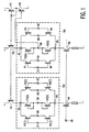
- FIG. 1 shows an embodiment of an electronic circuit with transconductors in accordance with the invention.
- the circuit comprises two transconductors TR1 and TR2.
- Each of the transconductors has input terminals IA and IB for receiving a differential input voltage, output terminals OA and OB for supplying a differential output current, a first node BA for receiving a first bias current, a second node BB for receiving a second bias current, and a common-mode terminal CM for supplying a common-mode voltage.
- Each of the transconductors further comprises: a PNP transistor pair comprising transistors P1 and P2 having their first main electrodes or emitters coupled to the first node BA, having their control electrodes or bases coupled to the input terminal IA and the input terminal IB, respectively, and having their second main electrodes or collectors coupled to the input terminal OA and the output terminal OB, respectively; an NPN transistor pair comprising transistors N1 and N2 having their emitters coupled to the second node BB, having their bases coupled to the input terminal IA and the input terminal IB, respectively, and having their collectors coupled to the output terminal OA and the output terminal OB, respectively; as well as a diode-connected PNP transistor P3 between the first node BA and the common-mode terminal CM, and a second diode-connected NPN transistor between the common-mode terminal CM and the second node BB.
- the emitter area of the transistor P3 is preferably 4 times as large as the emitter area of the transistors P1 and P2, as is indicated by the parenthesized figures.
- the NPN transistor pair N1, N2 of the transconductor TR1 receives bias current from an NPN current source transistor N4, which is connected between the second node BB and the negative supply voltage.
- An NPN transistor N5 performs the same function for the other transconductor TR2.
- the bases of the current source transistors N4 and N5 are connected to a voltage source VB, by means of which the bias currents of the transistors N4 and N5 are fixed.
- the PNP transistor pair P1, P2 of the transconductor TR1 receives bias current from a PNP current source transistor P4, which is connected between the first node BA and the positive supply voltage.
- a similarly arranged PNP transistor P5 supplies bias current to the first node BA of the transconductor TR2.
- the common-mode terminal CM of the transconductor TR2 is coupled to a diode-connected PNP transistor P7 via the base-emitter junction of a PNP transistor P6 arranged as an emitter-follower, the transistor P7 having its base-emitter junction arranged in parallel with that of the transistors P4 and P5.
- the transistors P4 and P5/P6/P7 together form a simple current mirror having an input branch, i.e. the transistors P5/P6/P7, and an output branch, i.e. the transistor P4.
- each transconductor is represented as a symbol with indications of the input terminals IA and IB, the output terminals OA and OB, the common-mode terminal CM and the first node BA.
- the biasing of the respective nodes BA of the transconductors with the transistors P4, P5, P6 and P7 is shown explicitly.
- the biasing of the respective nodes BB with the current source transistors N4 and N5 is not shown.
- the output terminals OA and OB of the transconductor TR1 are interconnected to the input terminals IA and IB of the transconductor TR2.
- the output terminals OA and OB of the transconductor TR2 are interconnected to the input terminals IA and IB, as a result of which the transconductor TR2 functions as a resistor which loads the transconductor TR1.
- the quiescent current through the transistor P1 also flows through the transistor N1.
- the nodes BA and BB were both energized with current sources having a fixed current intensity a problem would arise if these current sources do not supply equal currents and/or if the transistors P1/N1 and the transistors P2/N2 are not equally conductive for the same base voltage.
- the common-mode voltage component of the voltage between the output terminals OA and OB of the transconductor TR is indeterminate and, as a consequence, the transconductor TR2 coupled to the output terminals of the transconductor TR1 can end up in an undesirable DC operating range.
- the common-mode voltage can also be fed back to the common-mode terminal CM of the transconductor TR2 to the base of the transistor P5 in another manner than shown in Figure 1.
- the transistor P6 can alternatively be a diode-connected transistor having its emitter connected to the base of the transistor P5, in which case the transistor P7 is dispensed with. This again results in a constant voltage difference between the base and the collector of the transistor P5, which transistor then again functions as the input branch of the current mirror.
- the use of the diode-connected transistor P7 reduces the settling time of the common-mode control.
- the d.c. level on the input terminals IA and IB of the transconductor TR1 can be chosen freely.
- the transconductors are of a simple structure and can be used up to signal frequencies of a few hundreds of MHz.
- bipolar transistors instead of the bipolar transistors shown, it is possible to use unipolar (MOS) transistors, in which case base, emitter and collector should read gate, source and drain, respectively, and a diode-connected transistor is formed by interconnecting the gate and the drain.
- MOS unipolar
- the transistors chosen for the current source transistors may be of another type than the transistors in the transconductors, for example MOS transistors in the current source transistors and bipolar transistors in the transconductors or the other way round.
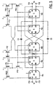
- FIG. 3 shows a first-order low-pass filter followed by a first-order all-pass filter.
- transconductors TR1..TR5 of which the transconductor TR1 has transconductance 2G and the other transconductors have a transconductance G.
- the input terminals IA and IB of the transconductor TR1 are connected to the filter input terminals FIA and FIB and the output terminals OA and OB of the transconductor TR5 are connected to the filter output terminals FOA and FOB.
- the output terminals OA and OB of the transconductor TR1 are connected to the output terminals OA and OB of the transconductor TR2;
- the input terminals IA and IB of the transconductor TR2 are connected to the input terminals IA and IB of the transconductor TR3;
- the input terminals IA and IB of the transconductor TR4 are connected to the input terminals IA and IB of the transconductor TR5.
- the output terminals OA and OB and the input terminals IA and IB of the transconductor TR2 are connected to one another and the output terminals OA and OB and the input terminals IA and IB of the transconductor TR5 are connected to one another.
- the output terminals OA and OB of the transconductor TR3 are connected to the input terminals IA and IB of the transconductor TR4 and the output terminals OA and OB of the transconductor TR4 are connected the other way round to the input terminals IA and IB of the transconductor TR3.
- a capacitor C1 having a capacitance 2Ca is connected across the input terminals IA and IB of the transconductor TR2.
- a capacitor C3 having a capacitance 2Cb is connected between the input terminal IA of the transconductor TR3 and the input terminal IA of the transconductor TR4; a capacitor C2 also having a capacitance 2Cb is connected between the input terminal IB of the transconductor TR3 and the input terminal IB of the transconductor TR4.
- Vo Vi G G + p . Ca G - p . Cb G + p . Cb
- the common-mode terminals CM of the transconductors TR2 and TR3 are interconnected and function as a reference for the bias of the respective nodes BA of the transconductors TR1, TR2 and TR4 via the current source transistors P8, P11 and P12, which form a current mirror with the diode-connected transistor P9, which is connected to the common-mode terminals CM of the transconductors TR2 and TR3 via a transistor P10.
- the common-mode terminals CM of the transconductors TR4 and TR5 are connected to one another and function as a reference for the bias of the respective nodes BA of the transconductors TR3 and TR5 via the current source transistors P13 and P14, which form a current mirror with the diode-connected transistor P15, which is connected to the common-mode terminals CM of the transconductors TR4 and TR5 via a transistor P16. Interconnection of the common-mode terminals CM of the transconductors TR2 and TR3 and of the transconductors TR4 and TR5 is possible because the inputs of these transconductors are at the same voltage.
- the area of the current source transistor P8 is twice as large as that of the other current source transistors in order to supply the transconductor TR1 with a quiescent current which is twice as large, so that this transconductor is given a transconductance which is twice as high as that of the other transconductors.
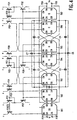
- FIG. 4 shows a second example of an application in a transconductor-C filter.
- This concerns a combination of a first-order low-pass filter and a second-order all-pass filter.
- the input terminals IA and IB of the transconductor TR1 are connected to the filter input terminals FIA and FIB and the output terminals OA and OB of the transconductor TR7 are connected to the filter output terminals FOA and FOB.
- the output terminals OA and OB of the transconductor TR1 are connected to the output terminals OA and OB of the transconductor TR2; the input terminals IA and IB of the transconductor TR2 are connected to the input terminals IA and IB of the transconductor TR3; the input terminals IA and IB of the transconductor TR4 are connected to the input terminals IA and IB of the transconductor TR5; the input terminals IA and IB of the transconductor TR6 are connected to the input terminals IA and IB of the transconductor TR7.
- the output terminals OA and OB and the input terminals IA and IB of the transconductor TR2 are connected to one another and the output terminals OA and OB and the input terminals IA and IB of the transconductor TR7 are connected to one another.
- the output terminals OA and OB of the transconductor TR3 are connected to the input terminals IA and IB of the transconductor TR4 and the output terminals OA and OB of the transconductor TR4 are connected the other way round to the input terminals IA and IB of the transconductor TR3; and the output terminals OA and OB of the transconductor TR5 are connected to the input terminals IA and IB of the transconductor TR6 and the output terminals OA and OB of the transconductor TR6 are connected the other way round to the input terminals IA and IB of the transconductor TR5.
- a capacitor C1 having a capacitance 2Cc is connected across the input terminals IA and IB of the transconductor TR2.
- a capacitor C3 having a capacitance 2Cd is connected between the input terminal IA of the transconductor TR3 and the input terminal IA of the transconductor TR4;
- a capacitor C2 also having a capacitance 2Cd is connected between the input terminal IB of the transconductor TR3 and the input terminal IB of the transconductor TR4;
- a capacitor C5 having a capacitance 2Ce is connected between the input terminal IA of the transconductor TR5 and the input terminal IA of the transconductor TR6;
- a capacitor C4 also having a capacitance 2Ce is connected between the input terminal IB of the transconductor TR5 and the input terminal IB of the transconductor TR6;
- a capacitor C7 having a capacitance 2Cf is connected between the input terminal IA of the transconductor TR3
- the common-mode terminals CM of the transconductors TR2 and TR3 are interconnected and function as a reference for the bias of the respective nodes BA of the transconductors TR1, TR2 and TR4 via the current source transistors P20, P23 and P24, which form a current mirror with the diode-connected transistor P21, which is connected to the common-mode terminals CM of the transconductors TR2 and TR3 via a transistor P22.
- the common-mode terminals CM of the transconductors TR4 and TR5 are connected to one another and function as a reference for the bias of the respective nodes BA of the transconductors TR3 and TR6 via the current source transistors P27 and P28, which form a current mirror with the diode-connected transistor P25, which is connected to the common-mode terminals CM of the transconductors TR4 and TR5 via a transistor P26.
- the common-mode terminals CM of the transconductors TR6 and TR7 are connected to one another and function as a reference for the bias of the respective nodes BA of the transconductors TR5 and TR7 via the current source transistors P29 and P30, which form a current mirror with the diode-connected transistor P31, which is connected to the common-mode terminals CM of the transconductors TR6 and TR7 via a transistor P32. Interconnection of the common-mode terminals CM of the transconductors TR2 and TR3, of the transconductors TR4 and TR5, and of the transconductors TR6 and TR7 is possible because the inputs of these transconductors are at the same voltage.
- the area of the current source transistor P20 is twice as large as that of the other current source transistors in order to supply the transconductor TR1 with a quiescent current which is twice as large, so that this transconductor is given a transconductance which is twice as high as that of the other transconductors.
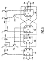
- Figure 5 shows a second-order low-pass filter.
- the input terminals IA and IB of the transconductor TR1 are connected to the filter input terminals FIA and FIB and the input terminals IA and IB of the transconductor TR4 are connected to the filter output terminals FOA and FOB.
- the output terminals OA and OB of the transconductor TR1 are connected to the output terminals OA and OB of the transconductor TR2; the input terminals IA and IB of the transconductor TR2 are connected to the input terminals IA and IB of the transconductor TR3; the input terminals IA and IB of the transconductor TR4 are connected to the output terminals OA and OB of the transconductor TR3.
- the output terminals OA and OB and the input terminals IA and IB of the transconductor TR2 are connected to one another.
- the output terminals OA and OB of the transconductor TR4 are connected the other way round to the input terminals IA and IB of the transconductor TR3.
- a capacitor C8 having a capacitance Cg is connected across the input terminals IA and IB of the transconductor TR2; and a capacitor C9 having a capacitance Ch is connected across the input terminals IA and IB of the transconductor TR4.
- Vo Vi G . G G . G + p . Ch . G + p . p . Cg . Ch
- the common-mode terminals CM of the transconductors TR2 and TR3 are interconnected and function as a reference for the bias of the respective nodes BA of the transconductors TR1 and TR2 via the current source transistors P33 and P36, which form a current mirror with the diode-connected transistor P34, which is connected to the common-mode terminals CM of the transconductors TR2 and TR3 via a transistor P35.
- the common-mode terminal CM of the transconductor TR4 functions as a reference for the bias of the respective nodes BA of the transconductors TR3 and TR4 via the current source transistors P37 and P40, which form a current mirror with the diode-connected transistor P38, which is connected to the common-mode terminal CM of the transconductor TR4 via a transistor P39. Interconnection of the common-mode terminals CM of the transconductors TR2 and TR3 is possible because the inputs of these transconductors are at the same voltage.
- FIG. 6 shows an oscillator with two transconductors TRA and TRB, which are again of the type as shown in Figure 1.
- the output terminals OA and OB of the transconductor TRA are connected to the input terminals IA and Ib of the transconductor TRB and the output terminals OA and OB of the transconductor TRB are connected the other way round to the input terminals IA and IB of the transconductor TRA.
- a capacitor C10 is connected across the input terminals IA and IB of the transconductor TRA and a capacitor C11 is connected across the input terminals IA and IB of the transconductor TRB.
- the oscillation frequency is equal to G/Co, Co being the capacitance of the capacitors C10 and C11.
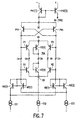
- Figure 7 shows the transconductor TRA of Figure 6.
- a PNP transistor P43 has its emitter, collector and base connected to a further node BC, the input terminal IA and the input terminal IB, respectively.
- a PNP transistor P43 has its emitter, collector and base connected to the node BC, the input terminal IB and the input terminal IA, respectively.
- the node BC is connected to the positive supply terminal via a diode-connected PNP transistor P41.
- the transistor P41 forms a current mirror with a PNP transistor P42, whose collector is connected to the node BA of the other transconductor TRB, which is identical to the transconductor TRA and which is not shown in Figure 7.
- the transconductor TRB consequently also comprises a transistor similar to the transistor P42, whose collector is connected to the node BA of the transconductor TRA.
- the emitter area of the transistor P42 is, for example, 3 times as large as that of the transistor P41.
- the input terminal IA is coupled to a current source CS1 via a diode-connected NPN transistor N6 and the input terminal IB is coupled to this current source via a diode-connected transistor N8.
- the ratio between the emitter areas of the transistors N6 and N8 is, for example, 3:1.
- the input terminal IA is coupled to a current source CS3 via a diode-connected NPN transistor N7 and the input terminal IB is coupled to this current source via a diode-connected transistor N9.
- the ratio between the emitter areas of the transistors N7 and N9 is, for example, 1:3.
- the node BB is coupled to a current source CS2, which supplies a bias current which is, for example, twice as large as that of the current sources CS1 and CS3.
- the transistors P43 and P44 provide attenuation equalization for small signals, so that the oscillator starts correctly.
- the transistors N6, N7, N8 and N9 and the current sources CS1 and CS2 together form a transconductor arranged as a resistor to provide attenuation for large signals, in order to limit the amplitude of such signals.
- the common-mode voltage is not measured on the terminal CM but on the further node BC.
- the transistors P43 and P44 now perform a double function, i.e. they provide attenuation equalization and they buffer a common-mode voltage. In this way, no extra current is required in order to achieve attenuation equalization.
Landscapes
- Engineering & Computer Science (AREA)
- Power Engineering (AREA)
- Amplifiers (AREA)
- Oscillators With Electromechanical Resonators (AREA)
- Inductance-Capacitance Distribution Constants And Capacitance-Resistance Oscillators (AREA)
- Networks Using Active Elements (AREA)
Claims (7)
- Circuit électronique comprenant une pluralité d'au moins un premier transconducteur (TR1) et un deuxième transconducteur (TR2), chacun comprenant des première (IA) et deuxième bornes d'entrée (IB) pour recevoir une tension différentielle et comprenant des première (OA) et deuxième bornes de sortie (OB) pour délivrer un courant différentiel en réponse à la tension différentielle, caractérisé en ce que chaque transconducteur du au moins premier transconducteur (TR1) et deuxième transconducteur (TR2) comprend:et en ce que le circuit électronique comprend encore:une première paire différentielle (P1, P2) de transistors d'un premier type de conductivité ayant leurs premières électrodes principales respectives les unes couplées aux autres dans un premier point commun (BA), ayant leurs deuxièmes électrodes principales respectives couplées à la première borne de sortie (OA) et à la deuxième borne de sortie (OB), et ayant leurs électrodes de commande respectives couplées à la première borne d'entrée (IA) et à la deuxième borne d'entrée (IB);une deuxième paire différentielle (N1, N2) de transistors d'un second type de conductivité qui est opposé au premier type de conductivité de la première paire différentielle (P1, P2), la deuxième paire différentielle ayant leurs premières électrodes principales respectives les unes couplées aux autres dans un deuxième point commun (BB), ayant leurs deuxièmes électrodes principales respectives couplées à la première borne de sortie (OA) et à la deuxième borne de sortie (OB), et ayant leurs électrodes de commande respectives couplées à la première borne d'entrée (IA) et à la deuxième borne d'entrée (IB);une première source de courant (P4) étant couplée au premier point commun (BA) pour délivrer un premier courant de polarisation à la première paire différentielle (P1, P2);une deuxième source de courant (N4) étant couplée au deuxième point commun (BB) pour délivrer un deuxième courant de polarisation à la deuxième paire différentielle (N1, N2);un premier transistor connecté en diode (P3) du premier type de conductivité et un deuxième transistor connecté en diode (N3) du second type de conductivité qui sont connectés en série entre le premier point commun (BA) et le deuxième point commun (BB);des moyens (P6, P7) pour commander la première source de courant (P4) d'au moins le premier transconducteur (TR1)en réponse à une tension de mode commun du deuxième transconducteur (TR2).
- Circuit électronique selon la revendication 1, caractérisé en ce que les moyens pour la commande comprennent:un miroir de courant (P4, P5) ayant une branche d'entrée (P5) couplée au premier point commun (BA) du deuxième transconducteur (TR2) et ayant des branches de sortie (P4) couplées à des premiers points communs respectifs (BA) d'au moins le premier transconducteur (TR1).
- Circuit électronique selon la revendication 2, caractérisé en ce que la branche d'entrée du miroir de courant comprend:un transistor de mesure (P6) du premier type de conductivité ayant une électrode de commande connectée à un point commun (CM) présent entre le premier transistor connecté en diode (P3) et le deuxième transistor connecté en diode (N3) du deuxième transconducteur(TR2);un nouveau autre transistor connecté en diode (P7) du premier type de conductivité qui est agencé en série à la première électrode principale du transistor de mesure (P6); etencore un nouveau autre transistor (P5) du premier type de conductivité ayant une électrode de commande et une première électrode principale qui sont agencées en parallèle à des électrodes correspondantes du nouveau autre transistor connecté en diode (P7) et ayant une deuxième électrode principale couplée au premier point commun (BA) du deuxième transconducteur (TR2).
- Circuit électronique selon la revendication 2 ou 3, caractérisé en ce que les points communs respectifs (CM) du premier transistor connecté en diode (P3) et du deuxième transistor connecté en diode (N3) d'un certain nombre de transistors de la pluralité de transconducteurs sont connectés les uns aux autres.
- Circuit électronique selon la revendication 1, caractérisé en ce que le premier (TRA) et le deuxième transconducteur (TRB) comprennent chacun encore:une nouvelle autre paire différentielle (P43, P44) de transistors du premier type de conductivité ayant des premières électrodes principales respectives les unes couplées aux autres dans un nouveau autre point commun (BC), ayant des deuxièmes électrodes principales respectives couplées à la première borne d'entrée (IA) et à la deuxième borne d'entrée (IB), et ayant des électrodes de commande respectives couplées à la deuxième borne d'entrée (IB) et à la première borne d'entrée (IA); etun miroir de courant (P41, P42) ayant une branche d'entrée (P41) couplée au nouveau autre point commun (BC) du premier transconducteur (TRA) et ayant une branche de sortie (P42) couplée au premier point commun (BA) du deuxième transconducteur (TRB).
- Circuit électronique selon la revendication 5, caractérisé en ce que le premier (TRA) et le deuxième transconducteur (TRB) comprennent chacun encore:une troisième source de courant (CS1) pour délivrer un troisième courant de polarisation;un troisième transistor connecté en diode (N6) du second type de conductivité qui est connecté entre la première borne d'entrée (IA) et la troisième source de courant (CS1);un quatrième transistor connecté en diode (N8) du second type de conductivité qui est connecté entre la deuxième borne d'entrée (IB) et la troisième source de courant (CS1);une quatrième source de courant (CS3) pour délivrer un quatrième courant de polarisation;un cinquième transistor connecté en diode (N7) du second type de conductivité qui est connecté entre la première borne d'entrée (IA) et la quatrième source de courant (CS3); etun sixième transistor connecté en diode (N9) du second type de conductivité qui est connecté entre la deuxième borne d'entrée (IB) et la quatrième source de courant (CS3).
- Circuit électronique selon la revendication 1, 2, 3, 4, 5 ou 6, caractérisé en ce que les dimensions du premier (P3) et du deuxième transistor connecté en diode (N3) sont quatre fois aussi élevées que celles des transistors de la première (P1, P2) et de la deuxième paire différentielle (N1, N2).
Priority Applications (1)
| Application Number | Priority Date | Filing Date | Title |
|---|---|---|---|
| EP97924199A EP0853839B1 (fr) | 1996-07-24 | 1997-06-17 | Circuit electronique comprenant des transducteurs complementaires pour filtres et oscillateurs |
Applications Claiming Priority (4)
| Application Number | Priority Date | Filing Date | Title |
|---|---|---|---|
| EP96202091 | 1996-07-24 | ||
| EP96202091 | 1996-07-24 | ||
| EP97924199A EP0853839B1 (fr) | 1996-07-24 | 1997-06-17 | Circuit electronique comprenant des transducteurs complementaires pour filtres et oscillateurs |
| PCT/IB1997/000708 WO1998004037A2 (fr) | 1996-07-24 | 1997-06-17 | Circuit electronique comprenant des transducteurs complementaires pour filtres et oscillateurs |
Publications (2)
| Publication Number | Publication Date |
|---|---|
| EP0853839A2 EP0853839A2 (fr) | 1998-07-22 |
| EP0853839B1 true EP0853839B1 (fr) | 2003-01-15 |
Family
ID=8224222
Family Applications (1)
| Application Number | Title | Priority Date | Filing Date |
|---|---|---|---|
| EP97924199A Expired - Lifetime EP0853839B1 (fr) | 1996-07-24 | 1997-06-17 | Circuit electronique comprenant des transducteurs complementaires pour filtres et oscillateurs |
Country Status (8)
| Country | Link |
|---|---|
| US (1) | US5859566A (fr) |
| EP (1) | EP0853839B1 (fr) |
| JP (1) | JP3875726B2 (fr) |
| KR (1) | KR100458143B1 (fr) |
| AT (1) | ATE231305T1 (fr) |
| DE (1) | DE69718433T2 (fr) |
| MY (1) | MY132523A (fr) |
| WO (1) | WO1998004037A2 (fr) |
Families Citing this family (5)
| Publication number | Priority date | Publication date | Assignee | Title |
|---|---|---|---|---|
| US6194949B1 (en) * | 1998-03-04 | 2001-02-27 | Nortel Networks Limited | Driver circuit for high speed data |
| GB2379814B (en) * | 2001-07-05 | 2003-10-29 | Zarlink Semiconductor Ltd | A mixer circuit arrangement and an image-reject mixer circuit arrangement |
| US6856197B1 (en) * | 2003-07-28 | 2005-02-15 | Electronic Topologies, Inc. | Symmetrical current amplifier |
| US6963244B1 (en) * | 2003-12-12 | 2005-11-08 | Analog Devices, Inc. | Common mode linearized input stage and amplifier topology |
| US7646244B1 (en) * | 2008-07-24 | 2010-01-12 | National Semiconductor Corporation | Apparatus and method for unity gain buffer with high switching speed and low quiescent current |
Family Cites Families (8)
| Publication number | Priority date | Publication date | Assignee | Title |
|---|---|---|---|---|
| US3870966A (en) * | 1973-06-01 | 1975-03-11 | Rca Corp | Complementary field effect transistor differential amplifier |
| US3991380A (en) * | 1976-02-09 | 1976-11-09 | Rca Corporation | Complementary field effect transistor differential amplifier |
| DD210147A1 (de) * | 1982-08-25 | 1984-05-30 | Univ Magdeburg Tech | Cmos-differenzverstaerker |
| CA1260080A (fr) * | 1986-09-10 | 1989-09-26 | Akira Yukawa | Circuit amplificateur operationnel a gamme de fonctionnement etendue |
| JPH023156A (ja) * | 1988-06-10 | 1990-01-08 | Mitsubishi Electric Corp | 差動増幅回路 |
| US5412343A (en) * | 1992-07-30 | 1995-05-02 | U.S. Philips Corporation | Common-mode signal sensor |
| US5550510A (en) * | 1994-12-27 | 1996-08-27 | Lucent Technologies Inc. | Constant transconductance CMOS amplifier input stage with rail-to-rail input common mode voltage range |
| US5631607A (en) * | 1995-09-06 | 1997-05-20 | Philips Electronics North America Corporation | Compact GM-control for CMOS rail-to-rail input stages by regulating the sum of the gate-source voltages constant |
-
1997
- 1997-06-17 WO PCT/IB1997/000708 patent/WO1998004037A2/fr not_active Ceased
- 1997-06-17 AT AT97924199T patent/ATE231305T1/de not_active IP Right Cessation
- 1997-06-17 DE DE69718433T patent/DE69718433T2/de not_active Expired - Lifetime
- 1997-06-17 JP JP50673498A patent/JP3875726B2/ja not_active Expired - Fee Related
- 1997-06-17 EP EP97924199A patent/EP0853839B1/fr not_active Expired - Lifetime
- 1997-06-17 KR KR10-1998-0702148A patent/KR100458143B1/ko not_active Expired - Fee Related
- 1997-07-14 US US08/891,821 patent/US5859566A/en not_active Expired - Lifetime
- 1997-07-22 MY MYPI97003311A patent/MY132523A/en unknown
Also Published As
| Publication number | Publication date |
|---|---|
| JP3875726B2 (ja) | 2007-01-31 |
| EP0853839A2 (fr) | 1998-07-22 |
| US5859566A (en) | 1999-01-12 |
| WO1998004037A3 (fr) | 1998-03-05 |
| MY132523A (en) | 2007-10-31 |
| KR20000064269A (ko) | 2000-11-06 |
| JPH11513228A (ja) | 1999-11-09 |
| KR100458143B1 (ko) | 2005-06-13 |
| DE69718433T2 (de) | 2003-10-30 |
| DE69718433D1 (de) | 2003-02-20 |
| ATE231305T1 (de) | 2003-02-15 |
| WO1998004037A2 (fr) | 1998-01-29 |
Similar Documents
| Publication | Publication Date | Title |
|---|---|---|
| US5182477A (en) | Bipolar tunable transconductance element | |
| KR970008536B1 (ko) | 로그변환회로 | |
| US5392003A (en) | Wide tuning range operational transconductance amplifiers | |
| US5880634A (en) | Wide band-width operational amplifier | |
| US4559502A (en) | Multi-stage amplifier with capacitive nesting for frequency compensation | |
| US5936445A (en) | PLL-based differential tuner circuit | |
| KR100299740B1 (ko) | 필터회로 | |
| GB2194697A (en) | Fully differential cmos operational power amplifier | |
| US5942929A (en) | Active phase splitter | |
| US5345190A (en) | Modular low voltage filter with common mode feedback | |
| CA2003401C (fr) | Circuit amplificateur a charge de reaction | |
| EP0579876A1 (fr) | Système pour l'accord de fréquences pour une pair d'amplificateurs opérationnels à transconductance-C | |
| CA1165829A (fr) | Amplificateur integre | |
| EP0286347A2 (fr) | Amplificateur différentiel à sortie équilibrée | |
| EP0438911A1 (fr) | Circuit de filtrage intégré | |
| EP0270156A1 (fr) | Dispositif de filtrage | |
| US4912427A (en) | Power supply noise rejection technique for amplifiers | |
| EP0052117B1 (fr) | Filtre actif biquadratique du mode courant | |
| EP0655831B1 (fr) | Amplificateur opérationnel de transconductance à haute performance intégrée à CMO | |
| EP0105911B1 (fr) | Circuit pour une source de signaux a haute impedance | |
| US20030038678A1 (en) | Differential amplifier with gain substantially independent of temperature | |
| US5859566A (en) | Electronic circuit comprising complementary transconductors for filters and oscillators | |
| US7265609B2 (en) | Transconductor circuits | |
| Chaichana et al. | Current-mode MISO filter using CCCDTAs and grounded capacitors | |
| US6031424A (en) | Differential amplifier with improved voltage gain using operational amplifiers to eliminate diode voltage drops |
Legal Events
| Date | Code | Title | Description |
|---|---|---|---|
| PUAI | Public reference made under article 153(3) epc to a published international application that has entered the european phase |
Free format text: ORIGINAL CODE: 0009012 |
|
| AK | Designated contracting states |
Kind code of ref document: A2 Designated state(s): AT DE FR GB NL |
|
| 17P | Request for examination filed |
Effective date: 19980907 |
|
| GRAG | Despatch of communication of intention to grant |
Free format text: ORIGINAL CODE: EPIDOS AGRA |
|
| 17Q | First examination report despatched |
Effective date: 20020404 |
|
| GRAG | Despatch of communication of intention to grant |
Free format text: ORIGINAL CODE: EPIDOS AGRA |
|
| GRAH | Despatch of communication of intention to grant a patent |
Free format text: ORIGINAL CODE: EPIDOS IGRA |
|
| GRAH | Despatch of communication of intention to grant a patent |
Free format text: ORIGINAL CODE: EPIDOS IGRA |
|
| GRAA | (expected) grant |
Free format text: ORIGINAL CODE: 0009210 |
|
| AK | Designated contracting states |
Kind code of ref document: B1 Designated state(s): AT DE FR GB NL |
|
| PG25 | Lapsed in a contracting state [announced via postgrant information from national office to epo] |
Ref country code: NL Free format text: LAPSE BECAUSE OF FAILURE TO SUBMIT A TRANSLATION OF THE DESCRIPTION OR TO PAY THE FEE WITHIN THE PRESCRIBED TIME-LIMIT Effective date: 20030115 Ref country code: AT Free format text: LAPSE BECAUSE OF FAILURE TO SUBMIT A TRANSLATION OF THE DESCRIPTION OR TO PAY THE FEE WITHIN THE PRESCRIBED TIME-LIMIT Effective date: 20030115 |
|
| REG | Reference to a national code |
Ref country code: GB Ref legal event code: FG4D |
|
| REF | Corresponds to: |
Ref document number: 69718433 Country of ref document: DE Date of ref document: 20030220 Kind code of ref document: P |
|
| NLV1 | Nl: lapsed or annulled due to failure to fulfill the requirements of art. 29p and 29m of the patents act | ||
| ET | Fr: translation filed | ||
| PLBE | No opposition filed within time limit |
Free format text: ORIGINAL CODE: 0009261 |
|
| STAA | Information on the status of an ep patent application or granted ep patent |
Free format text: STATUS: NO OPPOSITION FILED WITHIN TIME LIMIT |
|
| 26N | No opposition filed |
Effective date: 20031016 |
|
| REG | Reference to a national code |
Ref country code: GB Ref legal event code: 732E |
|
| REG | Reference to a national code |
Ref country code: FR Ref legal event code: TP |
|
| PGFP | Annual fee paid to national office [announced via postgrant information from national office to epo] |
Ref country code: FR Payment date: 20110727 Year of fee payment: 15 |
|
| PGFP | Annual fee paid to national office [announced via postgrant information from national office to epo] |
Ref country code: DE Payment date: 20110606 Year of fee payment: 15 |
|
| REG | Reference to a national code |
Ref country code: FR Ref legal event code: ST Effective date: 20130228 |
|
| REG | Reference to a national code |
Ref country code: DE Ref legal event code: R119 Ref document number: 69718433 Country of ref document: DE Effective date: 20130101 |
|
| PG25 | Lapsed in a contracting state [announced via postgrant information from national office to epo] |
Ref country code: FR Free format text: LAPSE BECAUSE OF NON-PAYMENT OF DUE FEES Effective date: 20120702 Ref country code: DE Free format text: LAPSE BECAUSE OF NON-PAYMENT OF DUE FEES Effective date: 20130101 |
|
| PGFP | Annual fee paid to national office [announced via postgrant information from national office to epo] |
Ref country code: GB Payment date: 20160527 Year of fee payment: 20 |
|
| REG | Reference to a national code |
Ref country code: GB Ref legal event code: PE20 Expiry date: 20170616 |
|
| PG25 | Lapsed in a contracting state [announced via postgrant information from national office to epo] |
Ref country code: GB Free format text: LAPSE BECAUSE OF EXPIRATION OF PROTECTION Effective date: 20170616 |