EP0854510A2 - Enlèvement d'un masque pour la gravure d'un sillon d'une capacité DRAM - Google Patents
Enlèvement d'un masque pour la gravure d'un sillon d'une capacité DRAM Download PDFInfo
- Publication number
- EP0854510A2 EP0854510A2 EP97310402A EP97310402A EP0854510A2 EP 0854510 A2 EP0854510 A2 EP 0854510A2 EP 97310402 A EP97310402 A EP 97310402A EP 97310402 A EP97310402 A EP 97310402A EP 0854510 A2 EP0854510 A2 EP 0854510A2
- Authority
- EP
- European Patent Office
- Prior art keywords
- layer
- hard mask
- mask
- pad
- substrate
- Prior art date
- Legal status (The legal status is an assumption and is not a legal conclusion. Google has not performed a legal analysis and makes no representation as to the accuracy of the status listed.)
- Withdrawn
Links
Images


Classifications
-
- H—ELECTRICITY
- H10—SEMICONDUCTOR DEVICES; ELECTRIC SOLID-STATE DEVICES NOT OTHERWISE PROVIDED FOR
- H10B—ELECTRONIC MEMORY DEVICES
- H10B12/00—Dynamic random access memory [DRAM] devices
- H10B12/30—DRAM devices comprising one-transistor - one-capacitor [1T-1C] memory cells
- H10B12/37—DRAM devices comprising one-transistor - one-capacitor [1T-1C] memory cells the capacitor being at least partially in a trench in the substrate
-
- H—ELECTRICITY
- H10—SEMICONDUCTOR DEVICES; ELECTRIC SOLID-STATE DEVICES NOT OTHERWISE PROVIDED FOR
- H10B—ELECTRONIC MEMORY DEVICES
- H10B12/00—Dynamic random access memory [DRAM] devices
- H10B12/01—Manufacture or treatment
- H10B12/02—Manufacture or treatment for one transistor one-capacitor [1T-1C] memory cells
- H10B12/03—Making the capacitor or connections thereto
- H10B12/038—Making the capacitor or connections thereto the capacitor being in a trench in the substrate
-
- H—ELECTRICITY
- H10—SEMICONDUCTOR DEVICES; ELECTRIC SOLID-STATE DEVICES NOT OTHERWISE PROVIDED FOR
- H10P—GENERIC PROCESSES OR APPARATUS FOR THE MANUFACTURE OR TREATMENT OF DEVICES COVERED BY CLASS H10
- H10P50/00—Etching of wafers, substrates or parts of devices
- H10P50/20—Dry etching; Plasma etching; Reactive-ion etching
- H10P50/28—Dry etching; Plasma etching; Reactive-ion etching of insulating materials
- H10P50/282—Dry etching; Plasma etching; Reactive-ion etching of insulating materials of inorganic materials
- H10P50/283—Dry etching; Plasma etching; Reactive-ion etching of insulating materials of inorganic materials by chemical means
Definitions
- the invention relates generally to DRAM structures and more particularly to a method for substantially preventing the undercutting of the pad oxide during the removal of the TEOS mask.
- Typical dynamic random access memories comprise multiple storage cells, each including a data storage capacitor and an access transistor. Such structures are used as semiconductor memories.
- DRAMs are generally implemented with one of two storage cell configurations.
- the first storage cell configuration comprises a "multilayer” capacitor structure formed on a semiconductor substrate.
- the other storage cell configuration comprises a “trench” capacitor structure formed on a semiconductor substrate. Since the "trench" capacitor structure allows for the highest density of memory cells per given area of semiconductor substrate, a preference for trench DRAM cells in various micro-electronic devices has been increasing steadily in recent years.
- a typical capacitance storage trench for a DRAM cell comprises a generally cylindrical-shaped trench that is etched into the surface of a semiconductor substrate.
- the trenches are typically created in the semiconductor substrate using a deep trench etch process such as reactive ion etching (RIE).
- RIE reactive ion etching
- a multilayer mask is deposited over the semiconductor substrate and patterned to enable the trenches to be selectively created in the appropriate areas of the semiconductor substrate. This is accomplished by first depositing a pad oxide layer over the semiconductor substrate. Next, a pad nitride layer is deposited over the pad oxide layer.
- the mask layer is completed by depositing a pad TEOS (tetra-ethyl-ortho-silicate) layer over the pad nitride layer and patterning the three pad layers using conventional techniques.
- the patterning of the mask layer exposes selected regions of the semiconductor substrate where the trenches are to be created.
- the pad TEOS serves as a RIE hard mask material for deep trench etching.
- portions of the pad nitride layer overhang the trenches and must be removed before further DRAM processing can take place. Further DRAM processing also requires the removal of the pad TEOS layer.
- the overhanging pad nitride portions and the pad TEOS layer are removed using two separately performed wet chemical isotropic etching procedures which produce a severe undercutting of the pad oxide and pad nitride layers.
- a process for removing a mask used for patterning device structures comprises providing a substrate of semiconductor material on which the device structures are formed.
- a mask is formed on the substrate.
- the mask comprises a hard mask layer and a hard mask etch stop layer below the hard mask layer.
- the mask layer is patterned to define a selected region. A portion of the substrate in the selected region is removed.
- an anisotropic dry process is performed to remove the portions of the hard mask layer that remains on the surface of the substrate.
- the anisotropic dry process such as a reactive ion etching, is selective to the hard mask etch stop layer.
- the RIE removes the hard mask layer without effectively removing the hard mask etch stop layer.
- the use of the RIE reduces the occurrence of undercutting in the remaining layers of the mask.
- the present invention relates generally to the fabrication of devices.
- the invention is directed to the reduction or elimination of undercutting of one of the pad layers, such as the pad oxide, that occurs during mask removal.
- the present invention is described in the context of a trench capacitor device.
- the invention is significantly broader and extends to the fabrication of devices where undercutting of a pad layer adversely affects subsequent process steps.
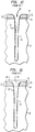
- a capacitance storage deep trench 20 for a DRAM cell is shown.
- the trench capacitor is formed by coventional patterning and etching techniques. Such techniques, for example, are described in Muller et al., Microelectronic Engineering , 27, p457 (1995); and Boudur et al., Extended Abstracts, Electrochem. Soc., Vol. 90-1 (May 1990), both herein incorporated by reference for all purposes.
- a conventional pad stack 12 is formed on the surface of a substrate 10.
- the pad stack serves as an etching mask.
- the mask is patterned so as to define regions wherein trenches are formed using, for example, conventional reactive ion etch (RIE) techniques.
- RIE reactive ion etch
- the pad stack comprises a pad oxide layer 14, a pad nitride layer 16, and pad TEOS layer 18.
- the pad TEOS layer provides a hard mask for the RIE
- the nitride layer serves as a polish stop for subsequent chemical mechanical polishing (CMP) step
- CMP chemical mechanical polishing
- a sidewall passivation film 24 is built up along the upper portion 22 of the trench sidewall 21 as a result of the RIE deep trench etch process.
- the edges of the TEOS layer defining the trench typically have a relatively higher exposure to the vertical bombardment of ions during the RIE than the planar portions of the TEOS layer. Higher exposure of ions increases the etch rate, resulting in faceted top corners 26 in the pad TEOS layer 18.
- the faceted top corners 26 cf the pad TEOS layer 18 can be tolerated as long as the facets 26 do not reach down to the underlying pad nitride layer 16. Facets in the pad nitride layer can detrimentally affect the chemical-mechanical polishing process that takes place later on in further DRAM processing.
- Fig. 1B shows the capacitance storage trench 20 of Fig. 1A after the removal of the sidewall passivation film 24 and the pulling back of a portion 31 of the pad nitride layer 16 which overhangs the opening of the deep trench 20 using a wet chemical process such as a dip in a buffered solution of hydrofluoric acid.
- the wet chemical process also tends to pull back the pad TEOS layer 18 at edges 28 and exposes a portion of the underlying pad nitride layer 16.
- the wet chemical process is isotropic, it also undercuts the pad oxide layer 14 shown at edges 30.
- Removal of the pad TEOS layer is achieved using a wet chemical process.
- removal of the pad TEOS undesirably causes further undercutting in the pad nitride layer.
- Further undercutting of the pad nitride layer leads to lifting off of the pad nitride layer and/or birds beak formation.
- undercutting of the pad nitride layer is avoided by delaying the removal of the pad TEOS layer until subsequent process steps have been completed. These subsequent process steps protect the exposed edges of the oxide layer, as will be apparent, from undercutting during an isotropic wet chemical process.
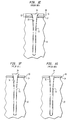
- a thin dielectric film or node dielectric layer 32 is formed along the entire surface of the deep trench using conventional thermal oxidation techniques.
- a polysilicon plug 34 is deposited using conventional techniques such as low pressure chemical vapor deposition, to fill the deep trench. The filling of the trench with polysilicon also forms a polysilicon layer 36 on the substrate surface.
- the surplus polysilicon layer 36 (shown in Fig. 1D) deposited during the formation of the polysilicon plug 34 from the polysilicon trench fill is removed by a chemical-mechanical polishing (CMP) step.
- CMP chemical-mechanical polishing
- the polysilicon plug 34 covers the pad oxide layer, thus protecting it from further undercutting caused by the wet chemical etching process. As such, removal of the pad TEOS layer 18 by a wet chemical process such as a hydrofluoric acid bath, can be achieved without detrimentally eroding the pad oxide layer.
- the polysilicon plug 34 extends out over the pad nitride layer 16. Accordingly, an additional CMP touch up is performed to planarize the substrate 10 as depicted in Fig. 1G.
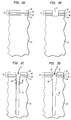
- Figs. 2A-2H show an embodiment of the invention.
- the invention enables the removal of the hard mask layer of the etch mask after formation of the deep trench without causing additional undercutting of the pad oxide layer. As previously discussed, such additional undercutting adversely affects subsequent process steps such as CMP.
- a pad stack 42 is formed on the surface of a semiconductor substrate 40 is shown.
- the pad stack serves as lithographic mask for defining and forming capacitance trench regions in the substrate.
- the pad stack comprises a plurality of pad films, including an adhesion promoting layer 44, a polish stop layer 46, a hard mask etch stop layer 48, and a hard mask layer 50, that are formed sequentially on the surface of the substrate.
- Various conventional techniques are useful for forming the pad films. These techniques, for example, include thermal oxidation and various chemical vapor deposition (CVD) techniques such as low pressure CVD (LPCVD), atmospheric-pressure (APCVD), and plasma-enhanced CVD (PECVD).
- CVD chemical vapor deposition
- LPCVD low pressure CVD
- APCVD atmospheric-pressure
- PECVD plasma-enhanced CVD
- the hard mask layer comprises a TEOS layer of sufficient thickness to prevent the RIE process for forming the deep trench from eroding the TEOS so as to expose the preceding layer.
- Other material such as boron doped silicate glass (BSG) is also useful.
- the TEOS layer is about 5000-7000 angstroms ( ⁇ ) thick.
- Beneath the hard mask layer is the hard mask etch stop layer 48.
- the hard mask etch stop layer enables the use of an anisotropic dry process, such as RIE.
- the RIE is slective to the hard mask etch stop layer, enabling the removal of the hard mask layer 50 without effectively removing the hard mask etch stop layer to prevent exposure of the preceding layers.
- the hard mask etch stop layer comprises a layer of polysilicon having a thickness sufficient to prevent exposure of the preceding pad films during the removal of the hard mask layer 50.
- the thickness of the etch stop layer is about 40-60 nanometers (nm).
- about a 50 nm polysilicon etch stop layer was sufficient to prevent exposure of the preceeding pad films while removing the TEOS hardmask having a thickness of, after the RIE process for forming the deep trench, about 50-250 nm.
- a RIE process selective to silicon nitride is performed to removed the TEOS layer.
- the use of the RIE selective to silicon nitride enables the pad nitride to serve as an etch stop layer during the removal of the TEOS layer, enabling the etch stop layer 48 between the TEOS layer 50 and the pad nitride layer 46 to be eliminated.
- the invention reduces the undercutting of the pad oxide layer 44 caused by conventional wet chemical process for removing of the hard mask layer 50.
- the polish stop layer 46 comprises a nitride layer formed by, for example, LPCVD.
- the thickness of the nitride layer is sufficient to prevent a polishing step, such as CMP, from exposing the underlying layer.
- the thickness of the nitride layer is about 200-240 nm, preferably about 220 nm.
- the adhesion promoting film comprises, for example, a thermally grown pad oxide layer having a thickness of about 70-120 ⁇ , preferably about 80 ⁇ .
- Fig. 2B depicts the substrate 40 of Fig. 2A after patterning the mask layer 42 using conventional photolithography techniques to remove a selected area 52 of the mask layer 42 to expose an underlying portion of the substrate 40 where the deep trench will be located.
- a deep trench 54 is formed in a conventional anisotropic RIE trench etch.
- a sidewall passivation film 60 is formed on the upper portion 58 of the trench sidewall 56 during the RIE trench etch.
- the sidewall passivation film is wet chemically removed by dipping in a buffered or diluted hydrofluoric acid.
- the duration of the acid dip is optimized to remove substantially only the sidewall passivation film.
- the remaining pad TEOS layer 50 is now removed using an anisotropic process such as a dry RIE etch process.
- the RIE is highly selective to the material of the pad etch stop layer (i.e. etches the material of the etch stop layer at a very low rate compared to TEOS).
- the pad etch stop layer comprises polysilicon
- the RIE is highly selective to polysilicon.
- the result of the RIE is depicted in Fig. 2E. Since the RIE etch process is anisotropic, only locations exposed to vertical ion bombardment are etched. No additional undercutting of the pad oxide layer 44 occurs because vertical ion bombardement is shadowed by the pad nitride layer 46.
- the sidewall passivation film can be removed simultaneously with the remaining pad TEOS layer during the dry RIE TEOS removal process if desired, thereby eliminating the need for the buffered hydrofluoric acid dip. Consequently, undercutting of the pad oxide layer 44 can be further reduced.
- Fig. 2F After dry removing the pad TEOS layer, further DRAM processing can be continued. More specifically as shown in Fig. 2F, this involves forming a thin dielectric film or node dielectric layer 64 along the entire surface of the deep trench 54 using conventional thermal oxidation techniques. Referring to Fig. 26, deep trench 54 is then filled with a polysilicon plug 66 using conventional techniques such as low pressure chemical vapor deposition. The deposition of polysilicon also forms a polysilicon layer 68. The surplus polysilicon layer 68 of the polysilicon plug 66 and the pad polysilicon layer 48 are removed by a chemical-mechanical polishing (CMP) step. Referring to FIG 2H, the resulting structure from the CMP step is shown.
- CMP chemical-mechanical polishing
Landscapes
- Engineering & Computer Science (AREA)
- Manufacturing & Machinery (AREA)
- Semiconductor Memories (AREA)
- Drying Of Semiconductors (AREA)
- Weting (AREA)
Applications Claiming Priority (2)
| Application Number | Priority Date | Filing Date | Title |
|---|---|---|---|
| US777156 | 1996-12-26 | ||
| US08/777,156 US5776808A (en) | 1996-12-26 | 1996-12-26 | Pad stack with a poly SI etch stop for TEOS mask removal with RIE |
Publications (2)
| Publication Number | Publication Date |
|---|---|
| EP0854510A2 true EP0854510A2 (fr) | 1998-07-22 |
| EP0854510A3 EP0854510A3 (fr) | 1999-09-08 |
Family
ID=25109444
Family Applications (1)
| Application Number | Title | Priority Date | Filing Date |
|---|---|---|---|
| EP97310402A Withdrawn EP0854510A3 (fr) | 1996-12-26 | 1997-12-22 | Enlèvement d'un masque pour la gravure d'un sillon d'une capacité DRAM |
Country Status (5)
| Country | Link |
|---|---|
| US (1) | US5776808A (fr) |
| EP (1) | EP0854510A3 (fr) |
| JP (1) | JPH10200076A (fr) |
| KR (1) | KR19980064673A (fr) |
| TW (1) | TW360976B (fr) |
Cited By (7)
| Publication number | Priority date | Publication date | Assignee | Title |
|---|---|---|---|---|
| EP0905749A3 (fr) * | 1997-09-30 | 2000-01-12 | Siemens Aktiengesellschaft | Réduction d'érosion de couches de masquage |
| WO2002031878A3 (fr) * | 2000-09-27 | 2002-10-31 | Infineon Technologies Corp | Procede permettant de proteger un oxyde de surface d'un groupe |
| EP1087423A3 (fr) * | 1999-09-24 | 2002-11-20 | Applied Materials, Inc. | Procédé de gravure de couches sur substrats, de nettoyage d'un réacteur d'attaque et dispositif correspondant |
| EP0932187A3 (fr) * | 1998-01-27 | 2003-02-26 | International Business Machines Corporation | Gravure des rainures utilisant un masque du verre borosilicate |
| EP0989598A3 (fr) * | 1998-09-25 | 2004-03-17 | Infineon Technologies AG | Procédé d'attaque par voie humide d'une structure à semiconducteurs |
| DE102004004879A1 (de) * | 2004-01-30 | 2005-08-25 | Infineon Technologies Ag | Maskierungsvorrichtung zur Maskierung beim Trockenätzen und Verfahren zur Herstellung einer Hartmaske |
| US9048301B2 (en) | 2013-10-16 | 2015-06-02 | Taiwan Semiconductor Manufacturing Company Limited | Nanowire MOSFET with support structures for source and drain |
Families Citing this family (24)
| Publication number | Priority date | Publication date | Assignee | Title |
|---|---|---|---|---|
| US5942449A (en) * | 1996-08-28 | 1999-08-24 | Micron Technology, Inc. | Method for removing an upper layer of material from a semiconductor wafer |
| US5955756A (en) * | 1997-05-29 | 1999-09-21 | International Business Machines Corporation | Trench separator for self-defining discontinuous film |
| US6013937A (en) * | 1997-09-26 | 2000-01-11 | Siemens Aktiengesellshaft | Buffer layer for improving control of layer thickness |
| US6020091A (en) * | 1997-09-30 | 2000-02-01 | Siemens Aktiengesellschaft | Hard etch mask |
| US5930645A (en) * | 1997-12-18 | 1999-07-27 | Advanced Micro Devices, Inc. | Shallow trench isolation formation with reduced polish stop thickness |
| US6200896B1 (en) | 1998-01-22 | 2001-03-13 | Cypress Semiconductor Corporation | Employing an acidic liquid and an abrasive surface to polish a semiconductor topography |
| US6143663A (en) * | 1998-01-22 | 2000-11-07 | Cypress Semiconductor Corporation | Employing deionized water and an abrasive surface to polish a semiconductor topography |
| US6121106A (en) * | 1998-03-11 | 2000-09-19 | International Business Machines Corporation | Method for forming an integrated trench capacitor |
| US6171180B1 (en) * | 1998-03-31 | 2001-01-09 | Cypress Semiconductor Corporation | Planarizing a trench dielectric having an upper surface within a trench spaced below an adjacent polish stop surface |
| US6232231B1 (en) | 1998-08-31 | 2001-05-15 | Cypress Semiconductor Corporation | Planarized semiconductor interconnect topography and method for polishing a metal layer to form interconnect |
| US5972124A (en) | 1998-08-31 | 1999-10-26 | Advanced Micro Devices, Inc. | Method for cleaning a surface of a dielectric material |
| US6534378B1 (en) | 1998-08-31 | 2003-03-18 | Cypress Semiconductor Corp. | Method for forming an integrated circuit device |
| US6566249B1 (en) | 1998-11-09 | 2003-05-20 | Cypress Semiconductor Corp. | Planarized semiconductor interconnect topography and method for polishing a metal layer to form wide interconnect structures |
| US6140206A (en) * | 1999-06-14 | 2000-10-31 | Chartered Semiconductor Manufacturing Ltd. | Method to form shallow trench isolation structures |
| US6232170B1 (en) * | 1999-06-16 | 2001-05-15 | International Business Machines Corporation | Method of fabricating trench for SOI merged logic DRAM |
| TW552669B (en) * | 2000-06-19 | 2003-09-11 | Infineon Technologies Corp | Process for etching polysilicon gate stacks with raised shallow trench isolation structures |
| US6969684B1 (en) | 2001-04-30 | 2005-11-29 | Cypress Semiconductor Corp. | Method of making a planarized semiconductor structure |
| US6613649B2 (en) * | 2001-12-05 | 2003-09-02 | Chartered Semiconductor Manufacturing Ltd | Method for buffer STI scheme with a hard mask layer as an oxidation barrier |
| US6828678B1 (en) | 2002-03-29 | 2004-12-07 | Silicon Magnetic Systems | Semiconductor topography with a fill material arranged within a plurality of valleys associated with the surface roughness of the metal layer |
| US7015115B1 (en) * | 2003-02-20 | 2006-03-21 | Newport Fab, Llc | Method for forming deep trench isolation and related structure |
| TWI227932B (en) * | 2003-06-23 | 2005-02-11 | Promos Technologies Inc | Method for forming a bottle-shaped trench |
| US7291541B1 (en) * | 2004-03-18 | 2007-11-06 | National Semiconductor Corporation | System and method for providing improved trench isolation of semiconductor devices |
| KR100688750B1 (ko) * | 2005-08-18 | 2007-03-02 | 동부일렉트로닉스 주식회사 | 섀로우 트렌치 아이솔레이션의 제조방법 |
| US9012296B2 (en) * | 2012-12-11 | 2015-04-21 | Taiwan Semiconductor Manufacturing Co., Ltd. | Self-aligned deep trench capacitor, and method for making the same |
Family Cites Families (5)
| Publication number | Priority date | Publication date | Assignee | Title |
|---|---|---|---|---|
| GB2200794A (en) * | 1986-11-19 | 1988-08-10 | Plessey Co Plc | Semiconductor device manufacture |
| US5118384A (en) * | 1990-04-03 | 1992-06-02 | International Business Machines Corporation | Reactive ion etching buffer mask |
| FR2669466B1 (fr) * | 1990-11-16 | 1997-11-07 | Michel Haond | Procede de gravure de couches de circuit integre a profondeur fixee et circuit integre correspondant. |
| US5593912A (en) * | 1994-10-06 | 1997-01-14 | International Business Machines Corporation | SOI trench DRAM cell for 256 MB DRAM and beyond |
| US5686345A (en) * | 1996-01-30 | 1997-11-11 | International Business Machines Corporation | Trench mask for forming deep trenches in a semiconductor substrate, and method of using same |
-
1996
- 1996-12-26 US US08/777,156 patent/US5776808A/en not_active Expired - Lifetime
-
1997
- 1997-12-22 EP EP97310402A patent/EP0854510A3/fr not_active Withdrawn
- 1997-12-23 TW TW086119585A patent/TW360976B/zh not_active IP Right Cessation
- 1997-12-25 JP JP9356623A patent/JPH10200076A/ja not_active Withdrawn
- 1997-12-26 KR KR1019970074008A patent/KR19980064673A/ko not_active Ceased
Cited By (11)
| Publication number | Priority date | Publication date | Assignee | Title |
|---|---|---|---|---|
| EP0905749A3 (fr) * | 1997-09-30 | 2000-01-12 | Siemens Aktiengesellschaft | Réduction d'érosion de couches de masquage |
| EP0932187A3 (fr) * | 1998-01-27 | 2003-02-26 | International Business Machines Corporation | Gravure des rainures utilisant un masque du verre borosilicate |
| EP0989598A3 (fr) * | 1998-09-25 | 2004-03-17 | Infineon Technologies AG | Procédé d'attaque par voie humide d'une structure à semiconducteurs |
| EP1087423A3 (fr) * | 1999-09-24 | 2002-11-20 | Applied Materials, Inc. | Procédé de gravure de couches sur substrats, de nettoyage d'un réacteur d'attaque et dispositif correspondant |
| US6802933B2 (en) | 1999-09-24 | 2004-10-12 | Anisul Khan | Apparatus for performing self cleaning method of forming deep trenches in silicon substrates |
| WO2002031878A3 (fr) * | 2000-09-27 | 2002-10-31 | Infineon Technologies Corp | Procede permettant de proteger un oxyde de surface d'un groupe |
| DE102004004879A1 (de) * | 2004-01-30 | 2005-08-25 | Infineon Technologies Ag | Maskierungsvorrichtung zur Maskierung beim Trockenätzen und Verfahren zur Herstellung einer Hartmaske |
| DE102004004879B4 (de) * | 2004-01-30 | 2008-03-13 | Qimonda Ag | Maskierungsvorrichtung zur Maskierung beim Trockenätzen und Verfahren zum Maskieren beim Trockenätzen eines zu strukturierenden Substrats |
| US9048301B2 (en) | 2013-10-16 | 2015-06-02 | Taiwan Semiconductor Manufacturing Company Limited | Nanowire MOSFET with support structures for source and drain |
| US9263295B2 (en) | 2013-10-16 | 2016-02-16 | Taiwan Semiconductor Manufacturing Company Limited | Nanowire MOSFET with support structures for source and drain |
| US9773868B2 (en) | 2013-10-16 | 2017-09-26 | Taiwan Semiconductor Manufacturing Company, Ltd. | Nanowire MOSFET with support structures for source and drain |
Also Published As
| Publication number | Publication date |
|---|---|
| US5776808A (en) | 1998-07-07 |
| KR19980064673A (ko) | 1998-10-07 |
| EP0854510A3 (fr) | 1999-09-08 |
| TW360976B (en) | 1999-06-11 |
| JPH10200076A (ja) | 1998-07-31 |
Similar Documents
| Publication | Publication Date | Title |
|---|---|---|
| US5776808A (en) | Pad stack with a poly SI etch stop for TEOS mask removal with RIE | |
| US5492858A (en) | Shallow trench isolation process for high aspect ratio trenches | |
| US6153474A (en) | Method of controllably forming a LOCOS oxide layer over a portion of a vertically extending sidewall of a trench extending into a semiconductor substrate | |
| US7087948B2 (en) | Forming electronic structures having dual dielectric thicknesses and the structure so formed | |
| EP0407047B1 (fr) | Méthode pour la planarisation de topologies pour des circuits intégrés | |
| US6194283B1 (en) | High density trench fill due to new spacer fill method including isotropically etching silicon nitride spacers | |
| US6171951B1 (en) | Dual damascene method comprising ion implanting to densify dielectric layer and forming a hard mask layer with a tapered opening | |
| US20030030121A1 (en) | Structure of trench isolation and a method of forming the same | |
| JPH0217637A (ja) | 高度に平面化された集積回路構造を作るための方法 | |
| US5728620A (en) | Isolation method of semiconductor device | |
| EP0609551B1 (fr) | Procédé de planarisation d'un dispositif semi-conducteur | |
| US6331472B1 (en) | Method for forming shallow trench isolation | |
| US6274426B1 (en) | Self-aligned contact process for a crown shaped dynamic random access memory capacitor structure | |
| US5641704A (en) | Method of isolating active areas of a semiconductor substrate by shallow trenches and narrow trenches | |
| US7410873B2 (en) | Method of manufacturing a semiconductor device | |
| US6551925B2 (en) | Method of forming a trench isolation structure resistant to hot phosphoric acid by extending trench liner to shoulder portions | |
| KR100244847B1 (ko) | 디봇 형성을 최소화하는 방법 및 집적 회로 칩 | |
| GB2372631A (en) | Semiconductor-on-insulator structure | |
| US6797636B2 (en) | Process of fabricating DRAM cells with collar isolation layers | |
| US6238997B1 (en) | Method of fabricating shallow trench isolation | |
| JP2622243B2 (ja) | 半導体素子のスタックキャパシター製造方法 | |
| KR20010008579A (ko) | 반도체장치의 sti형 소자분리막 형성방법 | |
| CN109994420A (zh) | 一种深槽隔离结构的制造方法 | |
| US6368973B1 (en) | Method of manufacturing a shallow trench isolation structure | |
| HK1015077A (en) | Mask removal for etching a dram capacitor trench |
Legal Events
| Date | Code | Title | Description |
|---|---|---|---|
| PUAI | Public reference made under article 153(3) epc to a published international application that has entered the european phase |
Free format text: ORIGINAL CODE: 0009012 |
|
| AK | Designated contracting states |
Kind code of ref document: A2 Designated state(s): DE FR GB IE IT NL |
|
| AX | Request for extension of the european patent |
Free format text: AL;LT;LV;MK;RO;SI |
|
| PUAL | Search report despatched |
Free format text: ORIGINAL CODE: 0009013 |
|
| RIC1 | Information provided on ipc code assigned before grant |
Free format text: 6H 01L 21/8242 A, 6H 01L 27/108 B, 6H 01L 21/308 B |
|
| AK | Designated contracting states |
Kind code of ref document: A3 Designated state(s): AT BE CH DE DK ES FI FR GB GR IE IT LI LU MC NL PT SE |
|
| AX | Request for extension of the european patent |
Free format text: AL;LT;LV;MK;RO;SI |
|
| 17P | Request for examination filed |
Effective date: 20000301 |
|
| AKX | Designation fees paid |
Free format text: DE FR GB IE IT NL |
|
| 17Q | First examination report despatched |
Effective date: 20001128 |
|
| RAP1 | Party data changed (applicant data changed or rights of an application transferred) |
Owner name: INTERNATIONAL BUSINESS MACHINES CORPORATION Owner name: INFINEON TECHNOLOGIES AG |
|
| REG | Reference to a national code |
Ref country code: HK Ref legal event code: WD Ref document number: 1015077 Country of ref document: HK |
|
| STAA | Information on the status of an ep patent application or granted ep patent |
Free format text: STATUS: THE APPLICATION IS DEEMED TO BE WITHDRAWN |
|
| 18D | Application deemed to be withdrawn |
Effective date: 20060701 |