EP0854555A2 - Protection d'alimentation intégré - Google Patents
Protection d'alimentation intégré Download PDFInfo
- Publication number
- EP0854555A2 EP0854555A2 EP97310049A EP97310049A EP0854555A2 EP 0854555 A2 EP0854555 A2 EP 0854555A2 EP 97310049 A EP97310049 A EP 97310049A EP 97310049 A EP97310049 A EP 97310049A EP 0854555 A2 EP0854555 A2 EP 0854555A2
- Authority
- EP
- European Patent Office
- Prior art keywords
- battery
- power source
- condition
- overvoltage
- transistor device
- Prior art date
- Legal status (The legal status is an assumption and is not a legal conclusion. Google has not performed a legal analysis and makes no representation as to the accuracy of the status listed.)
- Granted
Links
Images
Classifications
-
- H—ELECTRICITY
- H02—GENERATION; CONVERSION OR DISTRIBUTION OF ELECTRIC POWER
- H02H—EMERGENCY PROTECTIVE CIRCUIT ARRANGEMENTS
- H02H11/00—Emergency protective circuit arrangements for preventing the switching-on in case an undesired electric working condition might result
- H02H11/002—Emergency protective circuit arrangements for preventing the switching-on in case an undesired electric working condition might result in case of inverted polarity or connection; with switching for obtaining correct connection
- H02H11/003—Emergency protective circuit arrangements for preventing the switching-on in case an undesired electric working condition might result in case of inverted polarity or connection; with switching for obtaining correct connection using a field effect transistor as protecting element in one of the supply lines
-
- H—ELECTRICITY
- H02—GENERATION; CONVERSION OR DISTRIBUTION OF ELECTRIC POWER
- H02H—EMERGENCY PROTECTIVE CIRCUIT ARRANGEMENTS
- H02H9/00—Emergency protective circuit arrangements for limiting excess current or voltage without disconnection
- H02H9/04—Emergency protective circuit arrangements for limiting excess current or voltage without disconnection responsive to excess voltage
- H02H9/045—Emergency protective circuit arrangements for limiting excess current or voltage without disconnection responsive to excess voltage adapted to a particular application and not provided for elsewhere
- H02H9/046—Emergency protective circuit arrangements for limiting excess current or voltage without disconnection responsive to excess voltage adapted to a particular application and not provided for elsewhere responsive to excess voltage appearing at terminals of integrated circuits
Definitions
- the present invention relates generally to electrical power protection circuits, and more specifically to electrical power protection circuits as utilized in automotive applications.
- Overvoltage and reverse battery conditions are especially bad in that they can cause equipment damage when they occur.
- Power line conditioning in the prior art has been accomplished using discrete electrical components, integrated circuits, and hybrid implementations.
- Some power integrated circuits have overvoltage protection integrated on-chip, but in the prior art this has had the disadvantage of being very silicon consuming thereby adding cost.
- the integrated circuit signal power output stage also has to be designed to withstand these higher voltages with the result that certain device properties are degraded, such as Vce (sat) and Rds (on).
- additional extemal discrete components such as high-power zener diodes, have to be included to absorb voltage spikes that would otherwise damage other low voltage digital/analog circuitry present in the electrical circuit. These extemal components add size, cost and can increase power inefficiency.
- the aforementioned large currents which flow may damage the load, the power device and/or other electrical components in the circuit.
- a fuse Normally a fuse is inserted, although some discrete prior art solutions use a power MOSFET (Metal Oxide Silicon Field Effect Transistor) on either the supply line side or the ground line side.
- the power MOSFET is turned on during normal operation and tumed off during reverse battery conditions, interrupting current flow.
- a charge pump and logic circuitry is normally required.
- a charge pump may or may not be necessary depending on the minimum supply voltage, but some type of controlling circuitry is needed.
- a disadvantage of the prior art MOSFET approach for the ground side is undesirable ground bounce effects.
- an electrical power protection integrated circuit provides protection against reverse battery and overvoltage conditions that is particularly of value in automotive applications in which reverse battery and overvoltage conditions are commonplace.
- An electrical power protection integrated circuit contains a reverse battery condition protection element, supplied directly or indirectly from a battery power source, that protects against a reverse battery condition of the battery power source and an overvoltage protection element coupled to the reverse battery condition protection device that protects against an overvoltage condition of the battery power source and produces a protected power output that is isolated from both battery overvoltage and reverse battery voltage conditions. Additionally, the integrated circuit device can further produce an auxiliary protected power output that is isolated from reverse battery voltage conditions.
- the reverse battery condition protection element is supplied either directly or indirectly with a battery power source and has a first transistor device, such as a MOSFET, a first driver device coupled to the first transistor device that provides a constant voltage to the first transistor device during a normal operating condition of the electrical power protection circuit, and a switch coupled to the first transistor device and to the first driver device.
- a first transistor device such as a MOSFET
- a first driver device coupled to the first transistor device that provides a constant voltage to the first transistor device during a normal operating condition of the electrical power protection circuit
- a switch coupled to the first transistor device and to the first driver device.
- the overvoltage protection element is coupled to the reverse battery condition protection device and produces a protected power output and has a second transistor device coupled to the first transistor device that produces the protected power output, a second driver device coupled to the second transistor device that produces a voltage that is provided to the second transistor device, and a regulator device coupled to the second driver device.
- the overvoltage protection element operates to maintain the protected power output at a constant value that is isolated from the overvoltage condition of the battery power source.
- the second transistor device is regulated by the voltage produced by the second driver device that is made constant by the regulator device. Regulation of the second transistor device causes the second transistor device to enter a saturation region of operation so that the second transistor device operates to maintain the protected power output at the constant value.
- an electrical power protection circuit that provides protection against overvoltage and reverse battery voltage conditions, comprising a reverse battery condition protection element, supplied with a battery power source, that protects against a reverse battery condition of the battery power source, and an overvoltage protection element coupled to the reverse battery condition protection device that protects against an overvoltage condition of the battery power source and produces a protected power output.
- the reverse battery condition protection element may be inoperative so that no current flows from the battery power source to the overvoltage protection element thereby isolating the protected power output from the battery power source.
- the first transistor device during a normal operating condition of the electrical power protection circuit, and a switch coupled to the first transistor device and to the first driver device, wherein during the reverse battery condition of the battery power source, the first transistor device is turned off.
- the first transistor device may be turned off by the switch that provides a short condition between the battery power source and the constant voltage produced by the first driver device.
- the first transistor device may be a MOSFET transistor and the short condition between the battery power source and the constant voltage forces the gate to source voltage of the first transistor device to zero.
- the first transistor device may have a body diode.
- the switch may be a FET (Field Effect Transistor).
- the first driver device may be a regulated supply or a charge pump.
- the overvoltage protection element may operate to maintain the protected power output at a constant voltage that is isolated from the overvoltage condition of the battery power source.
- the overvoltage protection element may comprise a second transistor device, a second driver device coupled to the second transistor device that produces a voltage that is provided to the second transistor device, and a regulator device coupled to the second driver device, wherein during the overvoltage condition of the battery power source, the second transistor device is regulated by the voltage produced by the second driver device that is made constant by the regulator device and wherein regulation of the second transistor device causes the second transistor device to enter a saturation region of operation so that the second transistor device operates to maintain the protected power output at the constant voltage.
- the second transistor device may have a body diode.
- the second driver device may be a regulated supply or a charge pump.
- the regulator device may be replaced by a clamp device.
- the electrical power protection circuit may further comprise an auxiliary protected power output produced by the reverse battery condition protection element that is protected against a reverse battery condition of the battery power source.
- the reverse battery condition protection element may comprise a first transistor device, a first driver device coupled to the first transistor device that provides a constant voltage to the first transistor device during a normal operating condition of the electrical power protection circuit, and a switch coupled to the first transistor device and to the first driver device, and wherein the overvoltage protection element comprises a second transistor device, a second driver device coupled to the second transistor device that produces a voltage that is provided to the second transistor device, and a regulator device coupled to the second driver device.
- the reverse battery condition protection element may be inoperative so that no current flows from the battery power source to the overvoltage protection element thereby isolating the protected power output from the battery power source.
- the first transistor device may be turned off.
- the first transistor device may be turned off by the switch that provides a short condition between the battery power source and the constant voltage produced by the first driver device.
- the first transistor device may be a MOSFET transistor and the short condition between the battery power source and the constant voltage forces the gate to source voltage of the first transistor device to zero.
- the overvoltage protection element may operate to maintain the protected power output at a constant voltage that is isolated from the overvoltage condition of the battery power source.
- the second transistor device may be regulated by the voltage produced by the second driver device that is made constant by the regulator device and wherein regulation of the second transistor device causes the second transistor device to enter a saturation region of operation so that the second transistor device operates to maintain the protected power output at the constant voltage.
- the first transistor device may have a body diode and the second transistor device may have a body diode.
- the first transistor device may be a first MOSFET transistor and the second transistor device is a second MOSFET transistor.
- the electrical power protection circuit may be an integrated circuit.
- an electrical power protection integrated circuit that provides protection against overvoltage and reverse battery voltage conditions, comprising a reverse battery condition protection element, supplied with a battery power source, that protects against a reverse battery condition of the battery power source
- the reverse battery condition protection element comprises a first transistor device, supplied with a battery power source, a first driver device coupled to the first transistor device that provides a constant voltage to the first transistor device during a normal operating condition of the electrical power protection circuit, and a switch coupled to the first transistor device and to the first driver device, and an overvoltage protection element coupled to the reverse battery condition protection device that protects against an overvoltage condition of the battery power source and produces a protected power output
- the overvoltage protection element comprises a second transistor device coupled to the first transistor device that produces a protected power output, a second driver device coupled to the second transistor device that produces a voltage that is provided to the second transistor device, and a regulator device coupled to the second driver device.
- the reverse battery condition protection element may be inoperative so that no current flows from the battery power source to the overvoltage protection element thereby isolating the protected power output from the battery power source, and wherein during an overvoltage condition of the battery power source, the overvoltage protection element operates to maintain the protected power output at the constant voltage that is isolated from the overvoltage condition of the battery power source.
- the first transistor device may be turned off.
- the first transistor device may be turned off by the switch that provides a short condition between the battery power source and the constant voltage produced by the first driver device.
- the first transistor device may be a MOSFET transistor and the short condition between the battery power source and the constant voltage forces the gate to source voltage of the first transistor device to zero.
- the second transistor device may be regulated by the voltage produced by the second driver device that is made constant by the regulator device and wherein regulation of the second transistor device causes the second transistor device to enter a saturation region of operation so that the second transistor device operates to maintain the protected power output at the constant voltage.
- the first transistor device may have a body diode.
- the second transistor device may have a body diode.
- the switch may be a FET (Field Effect Transistor).
- the first driver device may be a regulated supply or a charge pump.
- the second driver device may be a regulated supply.
- the second driver device may be a charge pump and a clamp.
- the electrical power protection circuit may further comprise an auxiliary protected power output produced by the reverse battery condition protection element that is protected against a reverse battery condition of the battery power source.
- the first transistor device may be a first MOSFET transistor and the second transistor device may be a second MOSFET transistor.
- the present invention describes an integrated circuit that uses new and novel methods for providing a supply voltage that is fully protected against overvoltage and reverse battery conditions.
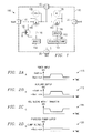
- FIG. 1 an overall block diagram 100 of the Electrical Power Protection Circuit 105 of the present invention is shown.
- the components of Electrical Power Protection Circuit 105 may be provided on an integrated circuit device and an integrated circuit implementation of the present invention addresses problems of the prior art.
- the power source, Vbatt is applied to Power Input 115 .
- the protected voltage output, Vprot is taken from Protected Power Output 120 .
- the normal current path is from Power Input 115 to First MOSFET Transistor 140 to Second MOSFET Transistor 145 to Protected Power Output 120 .
- First Body Diode 130 and Second Body Diode 135 are body diodes and are integral to First MOSFET Transistor 140 and Second MOSFET Transistor 145 , respectively, as shown.
- First MOSFET Transistor 140 and associated components First Driver 155 and Switch 150 are intended to protect against reverse battery conditions (Vbatt ⁇ 0).
- Second MOSFET Transistor 145 and associated components Second Driver 160 and Regulator/Clamp 165 protect against overvoltage conditions which may be present at Power Input 115 .
- Auxiliary Output 110 is provided to make available a power output which is only protected against reverse battery conditions.
- Ground 125 is the power ground for Electrical Power Protection Circuit 105 .
- Switch 150 provides the switching function whereby Power Input 115 and First Gate Voltage 170 are shorted when Vgnd>Vbatt, with these being not shorted otherwise.
- This switching function is basic and may be accomplished by means other than the FET illustrated for Switch 150 , as is well known in the art.
- First Driver 155 The purpose of First Driver 155 is to maintain a constant voltage at First Gate Voltage 170 so that First MOSFET Transistor 140 is always tumed on during normal operation.
- First Driver 155 would typically be a regulated supply or a charge pump, and various methods are known in the art to provide a constant voltage at First Gate Voltage 170 .
- the voltage at First Gate Voltage 170 will depend upon the device type and will have a value sufficient to ensure that First MOSFET Transistor 140 remains turned on.
- Second MOSFET Transistor 145 is clamped or regulated by the combination of Regulator/Clamp 165 , Regulator/Clamp Voltage 180 and Second Driver 160 to a constant value at Second Gate Voltage 185 .
- the result of an overvoltage condition at Auxiliary Output 110 and a constant Second Gate Voltage 185 is that Second MOSFET Transistor 145 enters the saturation region of operation wherein Protected Power Output 120 is maintained at a constant, but increased voltage.
- Second MOSFET Transistor 145 the increased voltage at Auxiliary Output 110 is absorbed by Second MOSFET Transistor 145 , appearing as an increase in the voltage differential across Second MOSFET Transistor 145 , which maintains Protected Power Output 120 essentially constant and isolated from the overvoltage condition at Power Input 115 .
- Second Driver 160 and Regulator/Clamp 165 are to maintain a constant voltage at Second Gate Voltage 185 so that Second MOSFET Transistor 140 is always tumed on during normal operation but is responsive to overvoltage conditions at Auxiliary Output 110 as previously discussed.
- Second Driver 160 would typically be a regulated supply or a charge pump, and Regulator/Clamp 165 is a regulator or voltage clamp.
- Second Gate Voltage 185 will typically depend upon the device type and will have a value sufficient to ensure that Second MOSFET Transistor 145 remains turned on as discussed previously.
- overvoltage protection mechanism As a more detailed explanation of the overvoltage protection mechanism of the present invention, note that an overvoltage condition at Power Input 115 will appear on Auxiliary Output 110 , since First MOSFET Transistor 140 is tumed on or will have First Body Diode 130 forward biased. If no action is taken, Protected Power Output 120 will follow Auxiliary Output 110 . If Second Gate Voltage 185 is maintained at a constant voltage (by Second Driver 160 and Regulator/Clamp 165 ), as Auxiliary Output 110 increases Protected Power Output 120 will try to follow which will produce a decrease in the Vgs of Second MOSFET Transistor 145 . This decrease in Vgs causes the Rds (on) of Second MOSFET Transistor 145 to increase which causes the voltage at Protected Power Output 120 to decrease. This is the mechanism whereby Vprot may be maintained at an essentially constant value.
- waveform A represents the voltage Vbatt present at Power Input 115 during an overvoltage transient condition. This voltage starts at nominal operating voltage Vbatt-nom, momentarily increasing to overvoltage Vbatt-ov before returning to Vbatt-nom.
- Waveform B represents the resulting voltage at Auxiliary Output 110 , and shows how the overvoltage condition is propagated from Power Input 115 to Auxiliary Output 110 .
- the voltage at Auxiliary Output 110 will be slightly less than Vbatt-ov by the forward voltage drop of First Body Diode 130 or First MOSFET Transistor 140 depending upon which device has the smaller voltage drop.
- Waveform C shows Vgs of Second MOSFET Transistor 145 during the overvoltage transient
- Waveform D shows how the voltage at Protected Power Output 120 is constrained during the transient.
- the voltage present at Protected Power Output 120 is [Vbatt-nom - lload(Rds (on total))] during normal operation, where lload is the current drawn by the load (not shown) attached to Protected Power Output 120 , and Rds (on) (drain to source resistance in an ON-state) total is the Rds (on) of Second MOSFET Transistor 145 summed with the Rds (on) of First MOSFET Transistor 140 .
- the maximum voltage at Protected Power Output 120 is limited by the value of the clamp voltage on Second Gate Voltage 185 .
- the present invention provides protection for electrical devices connected to Protected Power Output 120 from overvoltage and reverse battery voltage conditions which may be present on Power Input 115 .
- This allows a simplification of the circuitry of the electrical devices because they will never see overvoltage or reverse battery voltage conditions.
- the present invention provides this protection by a novel technique of blocking, not clamping, the overvoltage and reverse battery voltage conditions so as to isolate the protected output.
- the present invention realizes this protection on a single chip without the need for any external components by using a novel dual power MOSFET structure with back-to-back drains, along with associated control structures.
Landscapes
- Engineering & Computer Science (AREA)
- Microelectronics & Electronic Packaging (AREA)
- Charge And Discharge Circuits For Batteries Or The Like (AREA)
- Protection Of Static Devices (AREA)
- Emergency Protection Circuit Devices (AREA)
- Direct Current Feeding And Distribution (AREA)
- Semiconductor Integrated Circuits (AREA)
Applications Claiming Priority (2)
| Application Number | Priority Date | Filing Date | Title |
|---|---|---|---|
| US771644 | 1991-10-04 | ||
| US08/771,644 US5781390A (en) | 1996-12-21 | 1996-12-21 | Integrated supply protection |
Publications (3)
| Publication Number | Publication Date |
|---|---|
| EP0854555A2 true EP0854555A2 (fr) | 1998-07-22 |
| EP0854555A3 EP0854555A3 (fr) | 1999-09-01 |
| EP0854555B1 EP0854555B1 (fr) | 2003-07-09 |
Family
ID=25092517
Family Applications (1)
| Application Number | Title | Priority Date | Filing Date |
|---|---|---|---|
| EP97310049A Expired - Lifetime EP0854555B1 (fr) | 1996-12-21 | 1997-12-12 | Protection d'alimentation intégré |
Country Status (4)
| Country | Link |
|---|---|
| US (1) | US5781390A (fr) |
| EP (1) | EP0854555B1 (fr) |
| JP (1) | JPH10229639A (fr) |
| DE (1) | DE69723415T2 (fr) |
Cited By (8)
| Publication number | Priority date | Publication date | Assignee | Title |
|---|---|---|---|---|
| EP1193824A3 (fr) * | 2000-09-28 | 2005-06-22 | Delphi Technologies, Inc. | Circuit de protection contre l'inversion des bornes de la batterie |
| WO2006079422A1 (fr) * | 2005-01-26 | 2006-08-03 | Siemens Aktiengesellschaft | Circuit protecteur dans une entrée d'alimentation électrique d'un dispositif électrique et utilisation d'un circuit protecteur |
| FR2900421A1 (fr) * | 2006-04-27 | 2007-11-02 | Brandt Ind Sas | Procede d'optimisation du cycle de fonctionnement d'une machine a laver et machine a laver utilisant ledit procede |
| GB2459530A (en) * | 2008-04-28 | 2009-11-04 | Penny & Giles Controls Ltd | Transducer with an over-voltage protection circuit and voltage regulator |
| EP3113321A1 (fr) * | 2015-07-01 | 2017-01-04 | Carrier Corporation | Système et procédé de surveillance et de régulation de batteries parallèles |
| EP3226296A1 (fr) * | 2016-03-29 | 2017-10-04 | Nxp B.V. | Protection contre les décharges électrostatiques |
| US10424948B2 (en) | 2015-07-01 | 2019-09-24 | Carrier Corporation | Receptacle for monitoring and controlling parallel batteries |
| US11611209B2 (en) | 2019-05-02 | 2023-03-21 | Flash Electronics (India) Private Limited | System and a method for protecting a regulator rectifier device and a respective protection device |
Families Citing this family (37)
| Publication number | Priority date | Publication date | Assignee | Title |
|---|---|---|---|---|
| DE19719919A1 (de) * | 1997-05-13 | 1998-11-26 | Daimler Benz Ag | Anordnung zum Schutz von elektrischen Einrichtungen |
| US5923143A (en) * | 1998-03-20 | 1999-07-13 | York International Corporation | Solid state motor starter with energy recovery |
| US6008549A (en) * | 1999-03-19 | 1999-12-28 | Eldec Corporation | Solid-state high voltage switch and switching power supply |
| US6611410B1 (en) | 1999-12-17 | 2003-08-26 | Siemens Vdo Automotive Inc. | Positive supply lead reverse polarity protection circuit |
| US6628489B1 (en) * | 2000-05-31 | 2003-09-30 | Integration Associates Inc. | Battery and current reversal protect circuit |
| US7443229B1 (en) | 2001-04-24 | 2008-10-28 | Picor Corporation | Active filtering |
| US6985341B2 (en) * | 2001-04-24 | 2006-01-10 | Vlt, Inc. | Components having actively controlled circuit elements |
| JP2002335626A (ja) * | 2001-05-10 | 2002-11-22 | Nec System Technologies Ltd | 逆電流防止回路 |
| US6731486B2 (en) | 2001-12-19 | 2004-05-04 | Fairchild Semiconductor Corporation | Output-powered over-voltage protection circuit |
| US6580250B1 (en) | 2002-02-28 | 2003-06-17 | Dialog Semiconductor Gmbh | Monolithic battery protection circuit |
| US6882513B2 (en) * | 2002-09-13 | 2005-04-19 | Ami Semiconductor, Inc. | Integrated overvoltage and reverse voltage protection circuit |
| US20040141276A1 (en) * | 2002-10-25 | 2004-07-22 | Custer Robert J. | Electrical transient protection circuit |
| WO2004040761A1 (fr) * | 2002-10-29 | 2004-05-13 | Koninklijke Philips Electronics N.V. | Commutateur a deux transistors nmos bidirectionnel |
| US6970337B2 (en) * | 2003-06-24 | 2005-11-29 | Linear X Systems Inc. | High-voltage low-distortion input protection current limiter |
| US6898092B2 (en) * | 2003-06-25 | 2005-05-24 | Picor Corporation | EMI filter circuit |
| US6867640B2 (en) | 2003-07-01 | 2005-03-15 | Ami Semiconductor, Inc. | Double-sided extended drain field effect transistor, and integrated overvoltage and reverse voltage protection circuit that uses the same |
| US6967468B2 (en) * | 2003-07-02 | 2005-11-22 | Sigmatel, Inc. | Overvoltage and backflow current protection for a battery charger |
| EP1589651A1 (fr) * | 2004-04-23 | 2005-10-26 | STMicroelectronics S.r.l. | Dispositif pour alimenter des moteurs électriques |
| KR100601556B1 (ko) * | 2004-09-07 | 2006-07-19 | 삼성에스디아이 주식회사 | 이차 전지팩용 보호회로 |
| US7382594B2 (en) * | 2005-09-21 | 2008-06-03 | Semiconductor Components Industries, Llc | Method of forming an integrated voltage protection device and structure |
| JP5139022B2 (ja) * | 2007-10-15 | 2013-02-06 | ローム株式会社 | 過電圧保護回路ならびにそれを用いた電源管理回路および電子機器 |
| JP5086030B2 (ja) * | 2007-10-22 | 2012-11-28 | ローム株式会社 | 過電圧保護回路およびそれを用いた電子機器 |
| CN101656418B (zh) * | 2008-08-20 | 2012-12-12 | 台达电子工业股份有限公司 | 风扇系统及其电源逆向保护装置 |
| JP5411630B2 (ja) | 2009-09-03 | 2014-02-12 | ローム株式会社 | 負荷駆動装置 |
| US8143863B2 (en) * | 2009-10-12 | 2012-03-27 | O2Micro, Inc | Circuits and methods for controlling a current flowing through a battery |
| CN102570443B (zh) * | 2010-12-29 | 2014-12-03 | 广东易事特电源股份有限公司 | 一种太阳能充电控制器的防反接保护电路 |
| CN104247192A (zh) | 2012-04-23 | 2014-12-24 | 奥的斯电梯公司 | 蓄电池场断开方法 |
| US9472948B2 (en) * | 2013-09-30 | 2016-10-18 | Infineon Technologies Ag | On chip reverse polarity protection compliant with ISO and ESD requirements |
| US9564796B1 (en) | 2014-01-15 | 2017-02-07 | Western Digital Technologies, Inc. | Power circuit with overvoltage protection |
| US9768611B2 (en) * | 2015-02-18 | 2017-09-19 | Continental Automotive Systems, Inc. | Apparatus and method for reverse battery protection |
| FR3050586B1 (fr) * | 2016-04-22 | 2021-09-10 | Renault Sas | Protection de l’alimentation electrique d’un vehicule |
| JP7023561B2 (ja) * | 2016-08-30 | 2022-02-22 | エイブリック株式会社 | 充放電制御回路及びこれを備えたバッテリ装置 |
| JP7094181B2 (ja) * | 2018-08-29 | 2022-07-01 | 日清紡マイクロデバイス株式会社 | 負荷駆動回路 |
| JP7130495B2 (ja) * | 2018-08-29 | 2022-09-05 | 日清紡マイクロデバイス株式会社 | 負荷駆動回路 |
| US11522363B2 (en) * | 2018-09-03 | 2022-12-06 | Stmicroelectronics S.R.L. | Supply protection circuit that protects power transistor from a supply signal of an incorrect polarity |
| US11664741B2 (en) * | 2019-07-25 | 2023-05-30 | Susan Rhodes | System and method for AC power control |
| JP7587950B2 (ja) * | 2020-09-28 | 2024-11-21 | 日立建機株式会社 | 負荷駆動装置 |
Family Cites Families (5)
| Publication number | Priority date | Publication date | Assignee | Title |
|---|---|---|---|---|
| IT1226439B (it) * | 1988-07-05 | 1991-01-15 | Sgs Thomson Microelectronics | Circuito elettronico protetto da inversioni di polarita' della batteria di alimentazione. |
| US5196980A (en) * | 1991-01-28 | 1993-03-23 | John Fluke Mfg. Co., Inc. | Low impedance, high voltage protection circuit |
| US5410441A (en) * | 1993-02-01 | 1995-04-25 | Motorola, Inc. | Circuit for protecting DC powered devices from improper supply voltages |
| US5539610A (en) * | 1993-05-26 | 1996-07-23 | Siliconix Incorporated | Floating drive technique for reverse battery protection |
| US5434739A (en) * | 1993-06-14 | 1995-07-18 | Motorola, Inc. | Reverse battery protection circuit |
-
1996
- 1996-12-21 US US08/771,644 patent/US5781390A/en not_active Expired - Lifetime
-
1997
- 1997-12-12 DE DE1997623415 patent/DE69723415T2/de not_active Expired - Fee Related
- 1997-12-12 EP EP97310049A patent/EP0854555B1/fr not_active Expired - Lifetime
- 1997-12-16 JP JP9345994A patent/JPH10229639A/ja active Pending
Cited By (11)
| Publication number | Priority date | Publication date | Assignee | Title |
|---|---|---|---|---|
| EP1193824A3 (fr) * | 2000-09-28 | 2005-06-22 | Delphi Technologies, Inc. | Circuit de protection contre l'inversion des bornes de la batterie |
| WO2006079422A1 (fr) * | 2005-01-26 | 2006-08-03 | Siemens Aktiengesellschaft | Circuit protecteur dans une entrée d'alimentation électrique d'un dispositif électrique et utilisation d'un circuit protecteur |
| DE102005003682A1 (de) * | 2005-01-26 | 2006-08-24 | Siemens Ag | Schutzschaltung in einem Stromversorgungseingang einer elektrischen Einrichtung und Verwendung einer Schutzschaltung |
| FR2900421A1 (fr) * | 2006-04-27 | 2007-11-02 | Brandt Ind Sas | Procede d'optimisation du cycle de fonctionnement d'une machine a laver et machine a laver utilisant ledit procede |
| GB2459530A (en) * | 2008-04-28 | 2009-11-04 | Penny & Giles Controls Ltd | Transducer with an over-voltage protection circuit and voltage regulator |
| EP3113321A1 (fr) * | 2015-07-01 | 2017-01-04 | Carrier Corporation | Système et procédé de surveillance et de régulation de batteries parallèles |
| US10148099B2 (en) | 2015-07-01 | 2018-12-04 | Carrier Corporation | System and method for monitoring and controlling parallel batteries |
| US10424948B2 (en) | 2015-07-01 | 2019-09-24 | Carrier Corporation | Receptacle for monitoring and controlling parallel batteries |
| EP3226296A1 (fr) * | 2016-03-29 | 2017-10-04 | Nxp B.V. | Protection contre les décharges électrostatiques |
| US10164425B2 (en) | 2016-03-29 | 2018-12-25 | Nxp B.V. | Electrostatic discharge protection |
| US11611209B2 (en) | 2019-05-02 | 2023-03-21 | Flash Electronics (India) Private Limited | System and a method for protecting a regulator rectifier device and a respective protection device |
Also Published As
| Publication number | Publication date |
|---|---|
| DE69723415T2 (de) | 2004-05-06 |
| JPH10229639A (ja) | 1998-08-25 |
| EP0854555B1 (fr) | 2003-07-09 |
| DE69723415D1 (de) | 2003-08-14 |
| EP0854555A3 (fr) | 1999-09-01 |
| US5781390A (en) | 1998-07-14 |
Similar Documents
| Publication | Publication Date | Title |
|---|---|---|
| EP0854555B1 (fr) | Protection d'alimentation intégré | |
| US7324315B2 (en) | Protection device | |
| US6043965A (en) | Low loss reverse battery protection | |
| US5585991A (en) | Protective circuit for protecting load against excessive input voltage | |
| US7038522B2 (en) | System and method for redundant power supply connection | |
| US4930036A (en) | Electrostatic discharge protection circuit for an integrated circuit | |
| US6816348B2 (en) | Input protection circuit of a handheld electric device | |
| JP3610890B2 (ja) | 電気負荷駆動回路 | |
| EP0349836B1 (fr) | Circuit électronique protégé contre l'inversion de la polarité de sa batterie d'alimentation | |
| US4808839A (en) | Power field effect transistor driver circuit for protection from overvoltages | |
| EP0349837B1 (fr) | Circuit électronique muni d'un dispositif de protection contre des fluctuations de la tension de la batterie d'alimentation | |
| US7342433B2 (en) | Apparatus and method for enhanced transient blocking | |
| US7288856B2 (en) | Reverse battery protection circuit for power switch | |
| US20060023381A1 (en) | System and method for protecting a load from a voltage source | |
| US7492566B2 (en) | Low resistance transient blocking unit | |
| JPH10233632A (ja) | 高圧側mosfetゲート保護シャント回路 | |
| US8300373B2 (en) | Voltage triggered transient blocking unit | |
| US7327546B2 (en) | Power switching circuit with active clamp disconnect for load dump protection | |
| US20030086227A1 (en) | Device for protecting a power component against voltage surges | |
| US4839769A (en) | Driver protection circuit | |
| US6819535B2 (en) | Device for protecting loads supplied by an alternator | |
| US5488533A (en) | Methods and apparatus for isolating a power network from a load during an overcurrent condition | |
| US6061219A (en) | Device for the protection of an electrical load and power supply circuit having such a device | |
| US7408396B2 (en) | High voltage protection circuit | |
| US20060250736A1 (en) | Transient blocking apparatus with electrostatic discharge protection |
Legal Events
| Date | Code | Title | Description |
|---|---|---|---|
| PUAI | Public reference made under article 153(3) epc to a published international application that has entered the european phase |
Free format text: ORIGINAL CODE: 0009012 |
|
| AK | Designated contracting states |
Kind code of ref document: A2 Designated state(s): DE FR GB IT |
|
| AX | Request for extension of the european patent |
Free format text: AL;LT;LV;MK;RO;SI |
|
| RAP3 | Party data changed (applicant data changed or rights of an application transferred) |
Owner name: STMICROELECTRONICS, INC. |
|
| PUAL | Search report despatched |
Free format text: ORIGINAL CODE: 0009013 |
|
| RIC1 | Information provided on ipc code assigned before grant |
Free format text: 6H 02H 11/00 A, 6H 02H 9/04 B |
|
| AK | Designated contracting states |
Kind code of ref document: A3 Designated state(s): AT BE CH DE DK ES FI FR GB GR IE IT LI LU MC NL PT SE |
|
| AX | Request for extension of the european patent |
Free format text: AL;LT;LV;MK;RO;SI |
|
| 17P | Request for examination filed |
Effective date: 20000223 |
|
| AKX | Designation fees paid |
Free format text: DE FR GB IT |
|
| 17Q | First examination report despatched |
Effective date: 20020416 |
|
| GRAH | Despatch of communication of intention to grant a patent |
Free format text: ORIGINAL CODE: EPIDOS IGRA |
|
| GRAH | Despatch of communication of intention to grant a patent |
Free format text: ORIGINAL CODE: EPIDOS IGRA |
|
| GRAH | Despatch of communication of intention to grant a patent |
Free format text: ORIGINAL CODE: EPIDOS IGRA |
|
| GRAA | (expected) grant |
Free format text: ORIGINAL CODE: 0009210 |
|
| AK | Designated contracting states |
Designated state(s): DE FR GB IT |
|
| PG25 | Lapsed in a contracting state [announced via postgrant information from national office to epo] |
Ref country code: IT Free format text: LAPSE BECAUSE OF FAILURE TO SUBMIT A TRANSLATION OF THE DESCRIPTION OR TO PAY THE FEE WITHIN THE PRESCRIBED TIME-LIMIT;WARNING: LAPSES OF ITALIAN PATENTS WITH EFFECTIVE DATE BEFORE 2007 MAY HAVE OCCURRED AT ANY TIME BEFORE 2007. THE CORRECT EFFECTIVE DATE MAY BE DIFFERENT FROM THE ONE RECORDED. Effective date: 20030709 |
|
| REG | Reference to a national code |
Ref country code: GB Ref legal event code: FG4D |
|
| REF | Corresponds to: |
Ref document number: 69723415 Country of ref document: DE Date of ref document: 20030814 Kind code of ref document: P |
|
| PLBE | No opposition filed within time limit |
Free format text: ORIGINAL CODE: 0009261 |
|
| STAA | Information on the status of an ep patent application or granted ep patent |
Free format text: STATUS: NO OPPOSITION FILED WITHIN TIME LIMIT |
|
| ET | Fr: translation filed | ||
| 26N | No opposition filed |
Effective date: 20040414 |
|
| PGFP | Annual fee paid to national office [announced via postgrant information from national office to epo] |
Ref country code: DE Payment date: 20041209 Year of fee payment: 8 |
|
| PGFP | Annual fee paid to national office [announced via postgrant information from national office to epo] |
Ref country code: GB Payment date: 20051207 Year of fee payment: 9 |
|
| PGFP | Annual fee paid to national office [announced via postgrant information from national office to epo] |
Ref country code: FR Payment date: 20051208 Year of fee payment: 9 |
|
| PG25 | Lapsed in a contracting state [announced via postgrant information from national office to epo] |
Ref country code: DE Free format text: LAPSE BECAUSE OF NON-PAYMENT OF DUE FEES Effective date: 20060701 |
|
| GBPC | Gb: european patent ceased through non-payment of renewal fee |
Effective date: 20061212 |
|
| REG | Reference to a national code |
Ref country code: FR Ref legal event code: ST Effective date: 20070831 |
|
| PG25 | Lapsed in a contracting state [announced via postgrant information from national office to epo] |
Ref country code: GB Free format text: LAPSE BECAUSE OF NON-PAYMENT OF DUE FEES Effective date: 20061212 |
|
| PG25 | Lapsed in a contracting state [announced via postgrant information from national office to epo] |
Ref country code: FR Free format text: LAPSE BECAUSE OF NON-PAYMENT OF DUE FEES Effective date: 20070102 |