EP0857541A2 - Chemisch-mechanische Poliervorrichtung - Google Patents
Chemisch-mechanische Poliervorrichtung Download PDFInfo
- Publication number
- EP0857541A2 EP0857541A2 EP98101376A EP98101376A EP0857541A2 EP 0857541 A2 EP0857541 A2 EP 0857541A2 EP 98101376 A EP98101376 A EP 98101376A EP 98101376 A EP98101376 A EP 98101376A EP 0857541 A2 EP0857541 A2 EP 0857541A2
- Authority
- EP
- European Patent Office
- Prior art keywords
- pad
- wafer
- carrier
- polished
- chemical
- Prior art date
- Legal status (The legal status is an assumption and is not a legal conclusion. Google has not performed a legal analysis and makes no representation as to the accuracy of the status listed.)
- Withdrawn
Links
Images


Classifications
-
- B—PERFORMING OPERATIONS; TRANSPORTING
- B24—GRINDING; POLISHING
- B24B—MACHINES, DEVICES, OR PROCESSES FOR GRINDING OR POLISHING; DRESSING OR CONDITIONING OF ABRADING SURFACES; FEEDING OF GRINDING, POLISHING, OR LAPPING AGENTS
- B24B37/00—Lapping machines or devices; Accessories
- B24B37/27—Work carriers
- B24B37/30—Work carriers for single side lapping of plane surfaces
Definitions
- the present invention relates to a chemical and mechanical polishing (hereinafter simply referred to as CMP) apparatus for flattening or planarizing a surface of an object such as a wafer.
- CMP chemical and mechanical polishing
- ULSI ultra-large-scale integrated
- Fig. 11 is a sectional view showing one example of a surface flattening operation with such a CMP apparatus.
- the wafer 100 actually involves warpage and/or irregularities or variations in its thickness as shown in Fig. 12, however, it is quite difficult to flatten the wafer 100 by use of the CMP apparatus to any satisfactory extent.
- Fig. 13(a) is a sectional view showing surface flattening due to a so-called rear surface reference method.
- reference symbol 1 designates a carrier which has a holder 2 for holding an object to be polished in the form of a wafer 100 and a carrier shaft 3 fixedly coupled to a cone-shaped outer surface of the holder 2, the carrier 1 serving to firmly hold the wafer 100 on a surface plate 300 disposed under the carrier 1 during a polishing operation.
- a hard pad 200 made of foam urethane is attached or adhered to an inner surface of the holder 2 disposed on the opposite side of the carrier shaft 3.
- the hard pad 200 has a lot of holes 201 in communication with corresponding branches of an air passage 40 formed through the body of the holder 2 and the carrier shaft 3.
- a soft pad 210 and a hard polishing pad 220 are secured or adhered to an upper surface of the surface plate 300 in a laminated or stacked manner.
- the soft pad 210 may be in the form of a non-woven fabric pad such as one commercially available under the trade name of "Suba 400”
- the hard polishing pad 220 may be in the form of a polishing pad made of foam urethane such as one commercially available under the trade name of "IC 1,000".
- a lower surface of the hard pad 200 attached to the carrier 1 is made in contact with the wafer 100 so that air in a space between the lower surface of the hard pad 200 and the wafer 100 is evacuated through the air passage 40 in the carrier 1 by means of an unillustrated air pump connected to the air passage 40 whereby the wafer 100 is sucked or attracted under vacuum to the lower surface of the hard pad 200. Then, the wafer 100 thus fixedly held by the carrier 1 is transferred to a position over the hard polishing pad 220 of the surface plate 300, where the wafer 100 is made in contact at its lower surface with the hard polishing pad 220 through a downward motion of the carrier 1.
- the suction force applied to the wafer 100 is released, allowing the wafer 100 on the hard polishing pad 220 to move relative to the carrier 1 and hence the hard pad 200 with the result that the opposite surfaces of the wafer 100, which is being urged against the hard polishing pad 220 by means of a downward force or movement of the carrier 1, are polished by means of the hard polishing pad 220 of the rotating surface plate 300 and the hard pad 200 of the carrier 1 which is rotating in a direction opposite a rotational direction in which the surface plate 300 is rotating.
- the rear or second surface 100b of the wafer 100 is pressed so as to be flat by means of the hard pad 200, so that influences of warpage and/or irregularities in the thickness of the wafer 100 appear at the front or first surface 100a of the wafer 100.
- the hard polishing pad 220 is deflected together with the soft pad 210 along the curved contour of the front surface 100a.
- the surface 100a of the wafer 100 is polished by a constant thickness and flattened by means of the hard polishing pad 220.
- Fig. 13(b) is a sectional view showing surface flattening due to a so-called front surface reference method.
- a soft pad 230 in the form of a suede-type pad such as, for example, one commercially available under the trade name of "R200" which has a lot of through-holes 231 with which an air passage 40 is in communication through a plurality of corresponding branches in the holder 2.
- a hard polishing pad 220 is secured or adhered to the surface plate 300.
- the front surface 100a of the wafer 100 is urged or pushed so as to be flat by the hard polishing pad 220, and influences of warpage and/or irregularities in the thickness of the wafer 100 appear on its rear surface 100b.
- the soft pad 23 on the rear surface 100b of the wafer 100 the soft pad 230 is deformed along the curved contour of the rear surface 100b of the wafer 100. Consequently, the flat surface 100a of the wafer 100 is polished by a constant amount of thickness and thus flattened by means of the hard polishing pad 220.
- the first problem is that the elastic recovery rates of the hard pad 200 and the soft pad 230 attached to the holder 2 are low or poor. That is, the elastic recovery rate of the pad made of foam urethane used in general as the hard pad 200 is about 80%, so the foam urethane pad could not return to the original shape after a short period of use, and hence the duration or life thereof is short. Especially, the elastic recovery rate of "R200" used in general as the soft pad 230 varies within the range from 70% to 98% depending upon goods manufactured. Therefore, the soft pad 230 in the form of a product with a bad or low elastic recovery rate is not only of a short life, but also the polishing accuracy thereof will be deteriorated in a short period of use.
- the soft pad 230 elastically deforms along the curved contour of the rear surface 100b of the wafer 100 so as to allow the surface 100a of the wafer 100 to be subjected to a uniform pressure, whereby the wafer surface 100a can be polished in a uniform manner while being held in a substantially flat state.
- the soft pad 230 when the elasticity thereof has been deteriorated, can not deform along the curved contour of the rear surface 100b of the wafer 100, as a consequence of which the pressure or urging force applied from the soft pad 230 to the wafer 100 will become irregular or nonuniform, making the polishing speed of the wafer 100 different at portions thereof.
- the second problem is that a lot of dents or recesses in the shape of dimples are created on the surface 100a of the wafer 100. That is, through-holes 201, 231 of diameters in a range from 1 mm to 2 mm which communicate with the corresponding branches of the air passage 40 are formed through the hard pad 200 and the soft pad 230, as shown in Fig. 13(a) and Fig. 13(b).
- the third problem is that the wafer 100 might be dashed or flied out from the carrier 1 and damaged while the wafer 100 is polishing. That is, since the carrier 1 rotates at high speed while holding the wafer 100 with the surface plate 300 being also rotating, there might be the case that the wafer 100 occasionally happens to dash or fly out from the carrier 1 for some reason. In order to cope with this, it is preferred that air in the space between the wafer 100 and the pad 200 or 230 of the carrier 1 be evacuated or discharged through the through-holes 201 or 231 and the air passage 40 in the carrier 1 to thereby draw the wafer 100 against the carrier 1 even during polishing of the wafer 100. If, however, the drawing or suction force acts on the wafer 100 via through-holes 201 or 231, the dimple-shaped dents 100c in the wafer 100 grow deeper or greater, further worsening the surface state of the wafer 100.
- the fourth problem is that it is difficult to afford a desired magnitude of elasticity to the wafer 100.
- the apparatus is constructed such that it includes one hard pad 200 made of foam urethane, one soft pad 210 in the form of "Suba400", and one hard polishing pad 220 in the form of "IC1,000".
- the thickness of each pad is desired to be varied so as to change the amount of deformation thereof depending upon the kind or type of the wafer 100 to be polished.
- each of these pads is standardized and can not be varied, however, two or more hard pads 200 are used which are secured to the inner surface of the holder 2 in a laminated or stacked manner, and two or more soft pads 210 are secured to the surface of the surface plate 300 beneath the single hard polishing pad 220 similarly in a laminated or stacked manner.
- lamination of a plurality of pads each having a fixed or same thickness results in a discrete value of the total thickness of the pads, so it is difficult to set the total thickness of the laminated pads to a desired value, thus making it difficult to adjust a slight amount of deformation of the pads.
- the fifth problem is that the composition of the pad on the rear surface of the wafer 100 is changed by a polishing agent such as slurry. That is, chemical substances such as alkaline materials and acidic materials might be included in the slurry which is used as a polishing material, and the composition of the hard pad 200 or the soft pad 230 can be changed by such chemical substances, resulting in deformations and/or changes in the hardness and elasticity of the pad.
- a polishing agent such as slurry. That is, chemical substances such as alkaline materials and acidic materials might be included in the slurry which is used as a polishing material, and the composition of the hard pad 200 or the soft pad 230 can be changed by such chemical substances, resulting in deformations and/or changes in the hardness and elasticity of the pad.
- the present invention is intended to obviate the various problems as mentioned above, and has for its object to provide a novel and improved chemical and mechanical polishing apparatus which has a prolonged period of life and an improved accuracy in polishing, and which can prevent an object to be polished from inadvertently dashing out from a carrier and hence the resultant damage thereof, and in which the elasticity of a pressure pad can be adjusted to a desired magnitude of elasticity without any difficulty.
- a chemical and mechanical polishing apparatus comprising: a surface plate adapted to be rotatable and having a polishing pad attached thereto through a soft elastic pad; a carrier having a support surface for supporting an object to be polished which has a first surface and a second surface on the opposite sides thereof; a pressure pad attached to the support surface of the carrier for urging the object to be polished against the polishing pad, the pressure pad being formed of a thin porous elastic member so as to maintain the second surface of the object to be polished at a substantially flat state when urging the object against the polishing pad; and a holding means provided on the carrier for holding the object to be polished on the pressure pad; whereby the first surface of the object, which is urged from the second surface thereof into contact with the polishing pad of the surface plate by means of the carrier through the pressure pad, is polished by the rotating polishing pad.
- the object to be polished such as a wafer is held by the carrier through the pressure pad and urged toward the polishing pad by means of the carrier.
- the surface plate is driven to rotate while the object is being urged onto the polishing pad by means of the carrier, the rear surface of the object is maintained flat or planar by means of the thin pressure pad, and the soft elastic pad is deformed so that the surface of the wafer is uniformly pressed by the polishing pad.
- the holding means comprises an air passage which opens on the support surface of the carrier for drawing air.
- the thin porous elastic member has a multitude of minute pores.
- the thin porous elastic member comprises a trifluorochloroethylene resin.
- the surface of the wafer is maintained flat or planar by means of the thin trifluorochloroethylene resin so that when the holding means is operated, the wafer is sucked to the trifluorochloroethylene resin.
- the thin porous elastic member comprising a trifluorochloroethylene resin has a thickness of 5mm or less.
- that surface of the pressure pad which is in contact with the second surface of the object to be polished is a flat and smooth surface having substantially no irregularities.
- the rear surface of the wafer comes in contact with the flat and smooth surface of the pressure pad having substantially no convex, so there will be created no dimple or dent on the rear surface of the wafer due to these surface-to-surface contact.
- a chemical and mechanical polishing apparatus comprising: a surface plate adapted to be rotatable and having a polishing pad attached thereto through a soft elastic pad; a carrier having a support surface for supporting an object to be polished which has a first surface and a second surface on the opposite sides thereof; a pressure pad attached to the support surface of the carrier for urging the object to be polished against the polishing pad, the pressure pad being formed of a thick porous elastic member such that it is deformable along a contour of the second surface of the object to thereby maintain the second surface of the object to be polished at a substantially flat state when urging the object against the polishing pad; and a holding means provided on the carrier for holding the object to be polished on the pressure pad; whereby the first surface of the object, which is urged from the second surface thereof into contact with the polishing pad of the surface plate by means of the carrier through the pressure pad, is polished by the rotating polishing pad.
- the object to be polished such as a wafer is held by the carrier through the thick pressure pad and urged toward the polishing pad by means of the carrier.
- the surface plate is driven to rotate while the object is being urged onto the polishing pad by means of the carrier, the rear surface of the object is maintained flat or planar by means of the thick pressure pad, and the soft elastic pad is deformed so that the surface of the wafer is uniformly pressed by the polishing pad.
- the holding means comprises an air passage which opens on the support surface of the carrier for drawing air.
- the thick porous elastic member has a multitude of minute pores.
- the thick porous elastic member comprises a trifluorochloroethylene resin.
- the thick porous elastic member comprising a trifluorochloroethylene resin has a thickness of 8 mm or more.
- that surface of the pressure pad which is in contact with the second surface of the object to be polished is a flat and smooth surface having substantially no irregularities.
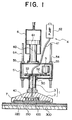
- Fig. 1 schematically illustrates the construction of a CMP apparatus in accordance with a first embodiment of the present invention.
- the CMP apparatus has a carrier 1, a holding means in the form of a suction mechanism 4, and a surface plate 300.
- the carrier 1 is rotatable about its own axis of rotation while holding an object to be polished such as a wafer 100.
- the carrier 1 is composed of a holder 2 for holding the wafer 100, and a carrier shaft 3 for supporting the holder 2 at its upper portion, as shown in Fig. 2.
- the holder 2 is provided at its lower portion with a pressure plate 20.
- An extension ring 21 is fitted over the outer peripheral surface of the pressure plate 20 in such a manner that it projects downward from a lower surface of the pressure plate 20 to thereby define a circular space 2a for receiving the wafer 100 at a location beneath the pressure plate 20.
- a housing 22 which is bolted to the pressure plate 20 and the extension ring 21 so as to integrally fasten these members.
- the carrier shaft 3 has a lower end fitted to and fixedly coupled to a central portion of an upper surface of the holder 2 and an upper end operatively connected with a drive means in the form of a motor 5, as shown in Fig. 1.
- a frame 51 mounted on an upper part of the carrier shaft 3 through an annular bearing 50 is a frame 51 to which the motor 5 is mounted.
- the motor 5 is provided with a gear 52 which is fixedly secured to a rotation shaft thereof.
- the gear 52 is in meshing engagement with a gear 53 which is fixedly mounted on the upper end of the carrier shaft 3.
- the rotational force or torque of the motor 5 is transmitted to the carrier 1 through the gears 52 and 53, so that the carrier 1 is caused to rotate on its own axis of rotation, i.e., about the central axis of the carrier shaft 3.
- the frame 51 is installed on vertically extending rails 54 through guide members 55 for free vertical motion relative thereto, with a cylinder 6 being connected with the frame 51.
- the cylinder 6 is vertically disposed and firmly supported by an unillustrated support member.
- the cylinder 6 has a piston 61 vertically slidably received therein with a piston rod 60 being connected at its upper end with the piston 61 and at its lower end with an upper surface of the frame 51.
- a pressure pad in the form of a Teflon layer 7 is attached or adhered to a lower surface of the carrier 1, which is driven to rotate by means of the motor 5 and pushed or urged against the surface plate 300 by the cylinder 6, for polishing the wafer 100 through a rear surface reference method.
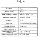
- Fig. 4 is a table chart in which the physical properties of the Teflon layer 7 are shown.
- the Teflon layer 7 is a porous elastic member formed of a trifluorochloroethylene resin. That is, the Teflon layer 7 contains 5,100 minute pores having a diameter of 3 ⁇ m per square centimeters, and its Young's modulus indicative of its elasticity is 50 kg/square millimeters, and its elastic recovery rate is 88% or more.
- Shore hardness D is 60 degrees, and very low as compared with the hardness of ceramic, silicon and the like.
- the thickness of the Teflon layer 7 having such physical properties is set to 5 mm.
- the Teflon layer 7 is adhered to the entire surface of a wafer support surface 20a which is the lower surface of the pressure plate 20, as shown in Fig. 2.
- the rear surface of the Teflon layer 7 is bonded to the wafer support surface or rear surface 20a of the pressure plate 20 through an epoxy-based adhesive.
- the adhesive is impregnated between the outer peripheral surface of the pressure plate 20 and the inner peripheral surface of the extension ring 21.
- a space defined between the pressure plate 20 and the extension ring 21 is kept airtight.
- the Teflon layer 7 is porous, air can be drawn from the front surface (lower-side surface in Fig. 2) of the Teflon layer 7.
- the surface of the Teflon layer 7 (i.e., the surface which is in contact with the wafer 100) is formed into a flat or planar surface without inclusion of convexes.
- the Teflon layer 7 is formed by solidifying Teflon particles 7a as shown in Fig. 5(a).
- the surface 7c of the Teflon layer 7 at the time of its manufacture is in an irregular or rugged state including a multitude of convexes and concaves owing to the Teflon particles 7a.
- the surface 7c of the Teflon layer 7 is polished or milled into a flat or smooth surface, as shown in Fig. 5(b).
- the surface of the Teflon layer 7 might be irregular or rugged including concaves and convexes. Therefore, in this case, too, the surface 7c of the Teflon layer 7 is made smooth or flat, as shown in Fig. 6(b).
- the suction mechanism 4 serves to attach the wafer 100 to the surface of the Teflon layer 7 by making effective use of the pores in the Teflon layer 7, and it comprises an air passage 40 formed in the holder 2, a tube 41 connected with the air passage 40, and a pump 42 which draws or suck air in the air passage 40 and the tube 41.
- the air passage 40 comprises a plurality of small-diameter passages or branches 40a formed in the pressure plate 20 so as to open on the wafer support surface 20a thereof, and a large-diameter passage 40b formed through the central portion of the housing 22 and connected with the small-diameter passages 40a.
- a hollow coupling member 40c is fitted to the top end of the large-diameter passage 40b.
- the tube 41 extending from the pump 42 is connected with the coupling member 40c.
- the surface plate 300 is operatively connected with an unillustrated drive means such as a motor so that it is thereby driven to rotate and polish the wafer 100.
- An elastic pad in the form of a soft pad 210 comprising a foamed pad commercially available under the trade name of "Suba400” is attached or adhered to an upper surface of the surface plate 300.
- a hard polishing pad 220 such as a plastic polishing pad commercially available under the trade name of "IC1,000” is adhered to an upper surface of the soft pad 210.
- the carrier 1 is lifted up by means of the cylinder 6 as shown in Fig. 1.
- the wafer 100 being polished which has previously been transported to an unillustrated location, is fitted into the circular space 2a inside the carrier 1, and then the pump 42 is energized to operate, so that air is evacuated from the pores in the Teflon layer 7 with which the wafer 100 is in abutment, so as to be drawn to the pump 42 by way of the air passage 40 in the carrier 1 and the tube 41.
- the insides of the pores in the Teflon layer 7 become vacuum, causing the wafer 100 to be sucked to the Teflon layer 7.
- the carrier 1 is moved downward by means of the cylinder 6 and driven to rotate by mean of the motor 5 to thereby push the wafer 100 onto the surface plate 300 while injecting an unillustrated polishing agent such as slurry into a space between the wafer 100 and the surface plate 300.
- an unillustrated polishing agent such as slurry into a space between the wafer 100 and the surface plate 300.
- the wafer 100 is forced to rotate with its surface 100a being pressed to the hard polishing pad 220 of the surface plate 300, whereby the wafer surface 100a is polished by the hard polishing pad 220.
- the wafer 100 rotating at a high speed does not dash or fly out from the carrier 1 because the wafer 100 is sucked or firmly attached to the carrier 1 under the action of a vacuum.
- the Teflon layer 7 is formed by solidifying Teflon particles 7a, as shown in Fig. 5(a), that surface of the wafer 100 which is in contact with the Teflon layer 7 is pressed or pushed by the Teflon particles 7a projecting from the surface 7c of the Teflon layer, so that there might be created a number of minute dimple-like recesses or dents 7on the surface of the wafer 100 in contact with the Teflon layer 7. Since the surface 7c of the Teflon layer 7 is polished to form a flat and smooth surface, as shown in Fig. 5(b), however, there will not be above-mentioned minute dimple-like recesses or dents developed on the surface of the wafer 100.
- the Teflon layer 7 elastically deforms.
- an elastic member having a thickness l and a Young's modulus E is deformed by an amount of deformation ⁇ I under the application of a pressure P, as shown in Fig. 7, so the following relation will be established: P/E : ⁇ I/I Therefore, when the pressure P of 500 g/cm 2 is applied to the Teflon layer 7 which has a Young's modulus E of 50 kg/mm 2 and a thickness l of 5 mm, the resultant amount of deformation ⁇ I of the Teflon layer 7 is very small.
- the wafer 100 does not sink or dent toward the Teflon layer 7 side, and the rear surface 100b of the wafer 100 is pressed directly by the pressure plate 20 so as to be flattened or planarized, as shown in Fig. 3.
- the warpage and/or irregularities in the thickness of the wafer 100 appear on its front surface 100a, which presses or pushes the hard polishing pad 220.
- the soft pad 210 which is provided beneath the hard polishing pad 220, is deformed so that the hard polishing pad 220 is deflected along the curved contour of the wafer surface 100a, as a consequence of which the warpage and/or irregularities or variations in the thickness of the wafer 100 are absorbed by the soft pad 210 and the hard polishing pad 220.
- the wafer 100 is polished with high accuracy according to the rear surface reference method.
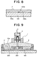
- agglomerated particles 100d of the polishing agent may occasionally invade inbetween the surface of the Teflon layer 7 and the rear surface 100b of the wafer 100 during the polishing operation, as shown in Fig. 8.
- Shore hardness D of the Teflon layer 7 is 60 degrees, which is smaller or lower than the hardness of ceramic, silicon or the like, so the Teflon layer 7 is dented, allowing the agglomerated particles 100d to sink in the Teflon layer 7. Accordingly, the pressure applied to the wafer 100 from the Teflon layer 7 is uniformly distributed over the entire rear surface 100b of the wafer 100 without concentrating on the agglomerated particles 100d, as a result of which there will be generated no wound or damage of the wafer 100 due to the agglomerated particles 100d.
- the polishing agent in the form of slurry which contains chemical substances such as alkaline materials or acidic materials during the wafer polishing operation adheres to the Teflon layer 7, but the Teflon layer 7 is strong or resistant to these chemical substances, so the composition thereof is not affected by these chemical substances and there will be no deformation of the Teflon layer 7, thus resulting in no change in the hardness and elasticity thereof.
- the rotations of the motor 5 and the surface plate 300 shown in Fig. 1 are stopped, and the carrier 1 having the thus polished wafer 100 sucked thereto is then raised by the cylinder 6 and transported to a predetermined storage place. Thereafter, the operation of the suction mechanism 4 is stopped, and the wafer 100 is released from the carrier 1 and stored in the storage place.
- the pressure pad formed of the Teflon layer 7 is much more durable for a long period of use as compared with a conventional pad, and hence the CMP apparatus according to this embodiment has a longer life.
- the Teflon layer 7 is not made of metal but of resin, there will neither be generation of metal contaminations or rust nor any wound or damage of the Teflon layer 7. For these reasons, the apparatus of the present invention is made long-lived.
- Fig. 9 shows in cross section a carrier as an essential portion of a CMP apparatus according to a second embodiment of the present invention.
- the CMP apparatus of this embodiment is different from the first-mentioned CMP apparatus according to the first embodiment in that a wafer 100 is polished according to a front surface reference method.
- a Teflon layer 7 ' of the same physical properties as those of the above-mentioned Teflon layer 7 of the first embodiment is attached or adhered to the wafer support surface 20a of the pressure plate 20.
- the thickness of this Teflon layer 7' is set to 5 mm so as to provide a greater amount of deformation than that of the above-mentioned Teflon layer 7 for the same pressure.
- the hard polishing pad 220 is attached or adhered directly on the surface plate 300.
- the surface 100a of the wafer 100 is made smooth or flat as shown in Fig. 10, and the warpage and/or irregularities or variations in the thickness of the wafer 100 appear on its rear surface 100b because the hard polishing pad 220 is adhered directly on the surface plate 300 .
- the thickness of the Teflon layer 7' on the rear surface 100b of the wafer 100 is set to 1.6 times the thickness of the Teflon layer 7 in the aforementioned first embodiment, so the amount of change or deformation ⁇ I of the Teflon layer 7' accordingly becomes 1.6 times that of the Teflon layer 7.
- the rear surface 100b of the wafer 100 sinks in the Teflon layer 7', so that the warpage and/or irregularities or variations in the thickness of the wafer 100 which appear on its rear surface 100b are absorbed by the Teflon layer 7'.
- the pressure or urging force of the carrier 1 can be uniformly applied to the rear surface 100b of the wafer 100, thus achieving highly accurate polishing of the wafer 100 according to the front surface reference method.
- the elastic member having a large amount of change or deformation as referred to above, when the elasticity thereof has been deteriorated, the rear surface 100b of the wafer 100 is not subjected to a uniform pressure. As a consequence, the front surface 100a of the wafer 100 is not held flat with a uniform pressure, thus inviting deterioration in the polishing accuracy.
- the Teflon layer 7' is high in the elastic recovery rate as referred to above, and hence the elasticity thereof can be maintained for a longer period of time as compared with a conventional pressure pad.
- the CMP apparatus is provided which can maintain the polishing accuracy for a long period of time.
- the thicknesses of the Teflon layers 7 and 7' are set to 5mm and 8mm, respectively, so as to provide predetermined amounts of elastic deformation, but in the case where it is desired to change the amounts of elastic deformation of the Teflon layers 7 and 7' depending upon the kind or type of the wafer 100, this can be achieved by changing the thicknesses of the Teflon layers 7 and 7' in an appropriate manner. That is, a slight adjustment of the deformation amount can be easily done by changing the thicknesses of the Teflon layers.
- the pressure pad is formed of a porous material having a multitude of minute pores, it is possible to prevent generation of dimple-like recesses or dents during a wafer is urged against the surface plate, thus improving the accuracy in polishing the wafer.
- the wafer can be attached or sucked to the pressure pad without generating recesses or dents on a surface of the wafer, so that it is possible to prevent the wafer from dashing out from the carrier during the wafer polishing operation.
- the pressure pad comprises an elastic member, when agglomerated particles of a polishing agent invade into a space between the wafer and the pressure pad, they are buried in the body of the pressure pad. As a result, a pressure or urging force can be applied uniformly to the wafer without concentrating on the agglomerated particles, whereby it is possible to prevent the wafer from being wound or damaged due to the invaded agglomerated particles.
- the amount of deformation of the pressure pad can be adjusted merely by changing the thickness of the pressure pad, so that a fine or slight adjustment of the deformation amount of the pressure pad can be done in a simple and easy manner.
- the elastic member having a multitude of minute pores, which constitutes the pressure pad is formed of trifluorochloroethylene, the elastic recovery rate of the pressure pad can be improved so it is possible to use the pressure pad for an extended period of time, thus prolonging the effective life of the apparatus.
- the trifluorochloroethylene resin is resistant to chemical substances such as alkaline or acidic materials, the composition of the resin is never affected or transformed by these chemical substances contained in the polishing agent or the like, and hence the life of the apparatus can be improved from this aspect.
Landscapes
- Engineering & Computer Science (AREA)
- Mechanical Engineering (AREA)
- Finish Polishing, Edge Sharpening, And Grinding By Specific Grinding Devices (AREA)
- Mechanical Treatment Of Semiconductor (AREA)
- Internal Circuitry In Semiconductor Integrated Circuit Devices (AREA)
Applications Claiming Priority (2)
| Application Number | Priority Date | Filing Date | Title |
|---|---|---|---|
| JP38427/97 | 1997-02-06 | ||
| JP3842797A JPH10217112A (ja) | 1997-02-06 | 1997-02-06 | Cmp装置 |
Publications (2)
| Publication Number | Publication Date |
|---|---|
| EP0857541A2 true EP0857541A2 (de) | 1998-08-12 |
| EP0857541A3 EP0857541A3 (de) | 1999-02-03 |
Family
ID=12525025
Family Applications (1)
| Application Number | Title | Priority Date | Filing Date |
|---|---|---|---|
| EP98101376A Withdrawn EP0857541A3 (de) | 1997-02-06 | 1998-01-27 | Chemisch-mechanische Poliervorrichtung |
Country Status (5)
| Country | Link |
|---|---|
| US (1) | US6030488A (de) |
| EP (1) | EP0857541A3 (de) |
| JP (1) | JPH10217112A (de) |
| KR (1) | KR19980071123A (de) |
| TW (1) | TW372901B (de) |
Cited By (3)
| Publication number | Priority date | Publication date | Assignee | Title |
|---|---|---|---|---|
| WO2000069595A3 (en) * | 1999-05-19 | 2001-02-01 | Speedfam Ipec Corp | Method and apparatus for automatically adjusting the contour of a wafer carrier surface |
| US6386956B1 (en) | 1998-11-05 | 2002-05-14 | Sony Corporation | Flattening polishing device and flattening polishing method |
| DE10009656B4 (de) * | 2000-02-24 | 2005-12-08 | Siltronic Ag | Verfahren zur Herstellung einer Halbleiterscheibe |
Families Citing this family (23)
| Publication number | Priority date | Publication date | Assignee | Title |
|---|---|---|---|---|
| JPH11138429A (ja) * | 1997-11-11 | 1999-05-25 | Sony Corp | 研磨装置 |
| JPH11204468A (ja) * | 1998-01-09 | 1999-07-30 | Speedfam Co Ltd | 半導体ウエハの表面平坦化装置 |
| US6340326B1 (en) | 2000-01-28 | 2002-01-22 | Lam Research Corporation | System and method for controlled polishing and planarization of semiconductor wafers |
| US6705930B2 (en) * | 2000-01-28 | 2004-03-16 | Lam Research Corporation | System and method for polishing and planarizing semiconductor wafers using reduced surface area polishing pads and variable partial pad-wafer overlapping techniques |
| JP4615813B2 (ja) * | 2000-05-27 | 2011-01-19 | ローム アンド ハース エレクトロニック マテリアルズ シーエムピー ホウルディングス インコーポレイテッド | 化学機械平坦化用の研磨パッド |
| US6652357B1 (en) | 2000-09-22 | 2003-11-25 | Lam Research Corporation | Methods for controlling retaining ring and wafer head tilt for chemical mechanical polishing |
| US6585572B1 (en) | 2000-08-22 | 2003-07-01 | Lam Research Corporation | Subaperture chemical mechanical polishing system |
| US7481695B2 (en) | 2000-08-22 | 2009-01-27 | Lam Research Corporation | Polishing apparatus and methods having high processing workload for controlling polishing pressure applied by polishing head |
| US6640155B2 (en) | 2000-08-22 | 2003-10-28 | Lam Research Corporation | Chemical mechanical polishing apparatus and methods with central control of polishing pressure applied by polishing head |
| US6471566B1 (en) | 2000-09-18 | 2002-10-29 | Lam Research Corporation | Sacrificial retaining ring CMP system and methods for implementing the same |
| US6443815B1 (en) | 2000-09-22 | 2002-09-03 | Lam Research Corporation | Apparatus and methods for controlling pad conditioning head tilt for chemical mechanical polishing |
| JP4009087B2 (ja) * | 2001-07-06 | 2007-11-14 | アプライド マテリアルズ インコーポレイテッド | 半導体製造装置における磁気発生装置、半導体製造装置および磁場強度制御方法 |
| US6530829B1 (en) * | 2001-08-30 | 2003-03-11 | Micron Technology, Inc. | CMP pad having isolated pockets of continuous porosity and a method for using such pad |
| US6736720B2 (en) | 2001-12-26 | 2004-05-18 | Lam Research Corporation | Apparatus and methods for controlling wafer temperature in chemical mechanical polishing |
| US6592437B1 (en) | 2001-12-26 | 2003-07-15 | Lam Research Corporation | Active gimbal ring with internal gel and methods for making same |
| US6937915B1 (en) | 2002-03-28 | 2005-08-30 | Lam Research Corporation | Apparatus and methods for detecting transitions of wafer surface properties in chemical mechanical polishing for process status and control |
| CA2519942A1 (en) | 2003-03-25 | 2004-10-14 | Neopad Technologies Corporation | Chip customized polish pads for chemical mechanical planarization (cmp) |
| US20070215280A1 (en) * | 2006-03-15 | 2007-09-20 | Sandhu Rajinder R | Semiconductor surface processing |
| JP5008922B2 (ja) * | 2006-07-31 | 2012-08-22 | セツ子 近藤 | ロアチャックパッド |
| US20080125021A1 (en) * | 2006-11-27 | 2008-05-29 | United Microelectronics Corp. | Disk holder and disk rotating device having the same |
| JP2010118424A (ja) * | 2008-11-12 | 2010-05-27 | Disco Abrasive Syst Ltd | 薄板状ワークの搬送装置 |
| US20180281151A1 (en) * | 2017-03-30 | 2018-10-04 | Applied Materials, Inc. | Adhesive-less carriers for chemical mechanical polishing |
| KR102783310B1 (ko) * | 2019-11-19 | 2025-03-19 | 가부시키가이샤 에바라 세이사꾸쇼 | 기판을 보유 지지하기 위한 톱링 및 기판 처리 장치 |
Family Cites Families (6)
| Publication number | Priority date | Publication date | Assignee | Title |
|---|---|---|---|---|
| JPS62297063A (ja) * | 1986-02-21 | 1987-12-24 | Hitachi Ltd | 薄片状部材研磨用真空チヤツク装置 |
| JPH01193166A (ja) * | 1988-01-28 | 1989-08-03 | Showa Denko Kk | 半導体ウェハ鏡面研磨用パッド |
| JPH03173129A (ja) * | 1989-12-01 | 1991-07-26 | Hitachi Ltd | 研磨装置 |
| JP2632738B2 (ja) * | 1990-04-27 | 1997-07-23 | 信越半導体 株式会社 | パッキングパッド、および半導体ウェーハの研磨方法 |
| JP3024373B2 (ja) * | 1992-07-07 | 2000-03-21 | 信越半導体株式会社 | シート状弾性発泡体及びウェーハ研磨加工用治具 |
| JP3463345B2 (ja) * | 1994-05-23 | 2003-11-05 | ソニー株式会社 | 研磨装置および研磨方法と張り合わせ方法 |
-
1997
- 1997-02-06 JP JP3842797A patent/JPH10217112A/ja active Pending
-
1998
- 1998-01-26 US US09/013,250 patent/US6030488A/en not_active Expired - Fee Related
- 1998-01-27 EP EP98101376A patent/EP0857541A3/de not_active Withdrawn
- 1998-02-05 TW TW087101462A patent/TW372901B/zh active
- 1998-02-06 KR KR1019980003370A patent/KR19980071123A/ko not_active Abandoned
Cited By (3)
| Publication number | Priority date | Publication date | Assignee | Title |
|---|---|---|---|---|
| US6386956B1 (en) | 1998-11-05 | 2002-05-14 | Sony Corporation | Flattening polishing device and flattening polishing method |
| WO2000069595A3 (en) * | 1999-05-19 | 2001-02-01 | Speedfam Ipec Corp | Method and apparatus for automatically adjusting the contour of a wafer carrier surface |
| DE10009656B4 (de) * | 2000-02-24 | 2005-12-08 | Siltronic Ag | Verfahren zur Herstellung einer Halbleiterscheibe |
Also Published As
| Publication number | Publication date |
|---|---|
| EP0857541A3 (de) | 1999-02-03 |
| JPH10217112A (ja) | 1998-08-18 |
| KR19980071123A (ko) | 1998-10-26 |
| US6030488A (en) | 2000-02-29 |
| TW372901B (en) | 1999-11-01 |
Similar Documents
| Publication | Publication Date | Title |
|---|---|---|
| US6030488A (en) | Chemical and mechanical polishing apparatus | |
| KR100876381B1 (ko) | 기판 고정 장치 및 기판 폴리싱 장치 | |
| US6390903B1 (en) | Precise polishing apparatus and method | |
| JP2002305168A (ja) | 研磨方法及び研磨装置および半導体装置の製造方法 | |
| KR20020032532A (ko) | 마이크로 전자 기판 조립체를 평탄화하기 위한 장치 및 방법 | |
| EP1691401A3 (de) | Cmp schleifmittel, verfahren ein substrat zu polieren und und verfahren zur herstellung von halbleiteranordnungen unter verwendung desselben und und zusatz zu einem cmp schleifmittel | |
| JPH0819960A (ja) | 軌道運動をする化学的機械的研磨装置 | |
| JP2001038604A (ja) | 可撓膜及びエッジロードリングを有するキャリヤヘッド | |
| JP4750250B2 (ja) | 変更された可撓膜を有するキャリアヘッド | |
| JP4666300B2 (ja) | 化学機械研磨システムの振動低減機能付キャリアヘッド | |
| US6443810B1 (en) | Polishing platen equipped with guard ring for chemical mechanical polishing | |
| JPH1086057A (ja) | 研磨装置とそのコンディショナ装置 | |
| JP2002113653A (ja) | 基板保持装置及び該基板保持装置を備えたポリッシング装置 | |
| TW200401359A (en) | Partial-membrane carrier head | |
| US6315649B1 (en) | Wafer mounting plate for a polishing apparatus and method of using | |
| JP2000334655A (ja) | Cmp加工装置 | |
| KR102078342B1 (ko) | 접촉 영역의 조절이 가능한 다이아몬드 컨디셔너 | |
| JP2002096261A (ja) | 基板保持装置及び該基板保持装置を備えたポリッシング装置 | |
| JPH06208980A (ja) | 研磨装置 | |
| JP3528501B2 (ja) | 半導体の製造方法 | |
| JPH11333677A (ja) | 基板の研磨装置 | |
| JP4503928B2 (ja) | 基板用研削装置 | |
| JP2001308049A (ja) | 基板加工における加工手段の移動速度の補正方法 | |
| US7229341B2 (en) | Method and apparatus for chemical mechanical polishing | |
| US6422929B1 (en) | Polishing pad for a linear polisher and method for forming |
Legal Events
| Date | Code | Title | Description |
|---|---|---|---|
| PUAI | Public reference made under article 153(3) epc to a published international application that has entered the european phase |
Free format text: ORIGINAL CODE: 0009012 |
|
| AK | Designated contracting states |
Kind code of ref document: A2 Designated state(s): DE FR GB NL |
|
| AX | Request for extension of the european patent |
Free format text: AL;LT;LV;MK;RO;SI |
|
| K1C1 | Correction of patent application (title page) published |
Effective date: 19980812 |
|
| PUAL | Search report despatched |
Free format text: ORIGINAL CODE: 0009013 |
|
| AK | Designated contracting states |
Kind code of ref document: A3 Designated state(s): AT BE CH DE DK ES FI FR GB GR IE IT LI LU MC NL PT SE |
|
| AX | Request for extension of the european patent |
Free format text: AL;LT;LV;MK;RO;SI |
|
| 17P | Request for examination filed |
Effective date: 19990115 |
|
| AKX | Designation fees paid |
Free format text: DE FR GB NL |
|
| 17Q | First examination report despatched |
Effective date: 20001108 |
|
| GRAG | Despatch of communication of intention to grant |
Free format text: ORIGINAL CODE: EPIDOS AGRA |
|
| RAP1 | Party data changed (applicant data changed or rights of an application transferred) |
Owner name: SPEEDFAM-IPEC INC. |
|
| GRAG | Despatch of communication of intention to grant |
Free format text: ORIGINAL CODE: EPIDOS AGRA |
|
| GRAH | Despatch of communication of intention to grant a patent |
Free format text: ORIGINAL CODE: EPIDOS IGRA |
|
| STAA | Information on the status of an ep patent application or granted ep patent |
Free format text: STATUS: THE APPLICATION IS DEEMED TO BE WITHDRAWN |
|
| 18D | Application deemed to be withdrawn |
Effective date: 20020301 |