EP0859065A1 - Legierungen auf Kupferbasis sowie Anschlusselementen - Google Patents
Legierungen auf Kupferbasis sowie Anschlusselementen Download PDFInfo
- Publication number
- EP0859065A1 EP0859065A1 EP98102539A EP98102539A EP0859065A1 EP 0859065 A1 EP0859065 A1 EP 0859065A1 EP 98102539 A EP98102539 A EP 98102539A EP 98102539 A EP98102539 A EP 98102539A EP 0859065 A1 EP0859065 A1 EP 0859065A1
- Authority
- EP
- European Patent Office
- Prior art keywords
- alloy
- terminals
- copper base
- spring
- stress relaxation
- Prior art date
- Legal status (The legal status is an assumption and is not a legal conclusion. Google has not performed a legal analysis and makes no representation as to the accuracy of the status listed.)
- Granted
Links
- 229910045601 alloy Inorganic materials 0.000 title claims abstract description 131
- 239000000956 alloy Substances 0.000 title claims abstract description 131
- 239000010949 copper Substances 0.000 title claims abstract description 61
- RYGMFSIKBFXOCR-UHFFFAOYSA-N Copper Chemical compound [Cu] RYGMFSIKBFXOCR-UHFFFAOYSA-N 0.000 title claims abstract description 46
- 229910052802 copper Inorganic materials 0.000 title claims abstract description 46
- 238000005452 bending Methods 0.000 claims abstract description 24
- 229910052759 nickel Inorganic materials 0.000 claims abstract description 16
- 229910052698 phosphorus Inorganic materials 0.000 claims abstract description 15
- 229910052718 tin Inorganic materials 0.000 claims abstract description 14
- 229910052725 zinc Inorganic materials 0.000 claims abstract description 7
- 239000000463 material Substances 0.000 claims description 25
- 239000002244 precipitate Substances 0.000 claims description 20
- 238000002844 melting Methods 0.000 claims description 16
- 230000008018 melting Effects 0.000 claims description 16
- 229910018104 Ni-P Inorganic materials 0.000 claims description 14
- 229910018536 Ni—P Inorganic materials 0.000 claims description 14
- 150000001875 compounds Chemical class 0.000 claims description 14
- 239000012535 impurity Substances 0.000 claims description 11
- 238000005097 cold rolling Methods 0.000 claims description 10
- 238000005098 hot rolling Methods 0.000 claims description 9
- 229910018886 Sn—Fe—P Inorganic materials 0.000 abstract description 10
- 229910000906 Bronze Inorganic materials 0.000 abstract description 9
- 239000010974 bronze Substances 0.000 abstract description 9
- KUNSUQLRTQLHQQ-UHFFFAOYSA-N copper tin Chemical compound [Cu].[Sn] KUNSUQLRTQLHQQ-UHFFFAOYSA-N 0.000 abstract description 9
- OAICVXFJPJFONN-UHFFFAOYSA-N Phosphorus Chemical compound [P] OAICVXFJPJFONN-UHFFFAOYSA-N 0.000 abstract description 7
- 238000003780 insertion Methods 0.000 abstract description 7
- 230000037431 insertion Effects 0.000 abstract description 7
- 238000000605 extraction Methods 0.000 abstract description 5
- 229910009038 Sn—P Inorganic materials 0.000 abstract description 2
- PXHVJJICTQNCMI-UHFFFAOYSA-N nickel Substances [Ni] PXHVJJICTQNCMI-UHFFFAOYSA-N 0.000 description 55
- 238000012360 testing method Methods 0.000 description 27
- 230000002180 anti-stress Effects 0.000 description 20
- 238000010438 heat treatment Methods 0.000 description 17
- 238000013508 migration Methods 0.000 description 16
- 229910001369 Brass Inorganic materials 0.000 description 10
- 239000010951 brass Substances 0.000 description 10
- 230000000694 effects Effects 0.000 description 8
- 239000011701 zinc Substances 0.000 description 8
- 230000007423 decrease Effects 0.000 description 7
- 238000004519 manufacturing process Methods 0.000 description 6
- 230000007797 corrosion Effects 0.000 description 5
- 238000005260 corrosion Methods 0.000 description 5
- 238000005336 cracking Methods 0.000 description 5
- 239000013078 crystal Substances 0.000 description 4
- 230000003247 decreasing effect Effects 0.000 description 4
- 230000001771 impaired effect Effects 0.000 description 4
- 238000000034 method Methods 0.000 description 4
- 230000005012 migration Effects 0.000 description 4
- 239000000203 mixture Substances 0.000 description 4
- 238000007747 plating Methods 0.000 description 4
- 229920000122 acrylonitrile butadiene styrene Polymers 0.000 description 3
- 239000011159 matrix material Substances 0.000 description 3
- 238000005259 measurement Methods 0.000 description 3
- 238000005554 pickling Methods 0.000 description 3
- 238000001556 precipitation Methods 0.000 description 3
- 230000009467 reduction Effects 0.000 description 3
- 229920006395 saturated elastomer Polymers 0.000 description 3
- 239000004809 Teflon Substances 0.000 description 2
- 229920006362 Teflon® Polymers 0.000 description 2
- 239000000853 adhesive Substances 0.000 description 2
- 230000001070 adhesive effect Effects 0.000 description 2
- 238000005266 casting Methods 0.000 description 2
- 230000006872 improvement Effects 0.000 description 2
- 239000000155 melt Substances 0.000 description 2
- 238000012856 packing Methods 0.000 description 2
- 238000000926 separation method Methods 0.000 description 2
- 239000008399 tap water Substances 0.000 description 2
- 235000020679 tap water Nutrition 0.000 description 2
- 229910017518 Cu Zn Inorganic materials 0.000 description 1
- 229910017752 Cu-Zn Inorganic materials 0.000 description 1
- 229910017943 Cu—Zn Inorganic materials 0.000 description 1
- 229910000640 Fe alloy Inorganic materials 0.000 description 1
- ATJFFYVFTNAWJD-UHFFFAOYSA-N Tin Chemical compound [Sn] ATJFFYVFTNAWJD-UHFFFAOYSA-N 0.000 description 1
- 229910001315 Tool steel Inorganic materials 0.000 description 1
- 229910001297 Zn alloy Inorganic materials 0.000 description 1
- 230000008901 benefit Effects 0.000 description 1
- 230000000052 comparative effect Effects 0.000 description 1
- 239000004020 conductor Substances 0.000 description 1
- 238000007796 conventional method Methods 0.000 description 1
- TVZPLCNGKSPOJA-UHFFFAOYSA-N copper zinc Chemical compound [Cu].[Zn] TVZPLCNGKSPOJA-UHFFFAOYSA-N 0.000 description 1
- 230000008878 coupling Effects 0.000 description 1
- 238000010168 coupling process Methods 0.000 description 1
- 238000005859 coupling reaction Methods 0.000 description 1
- 230000007547 defect Effects 0.000 description 1
- 230000001419 dependent effect Effects 0.000 description 1
- 230000006866 deterioration Effects 0.000 description 1
- 238000005516 engineering process Methods 0.000 description 1
- 230000020169 heat generation Effects 0.000 description 1
- -1 i.e. Substances 0.000 description 1
- 230000000977 initiatory effect Effects 0.000 description 1
- 239000002184 metal Substances 0.000 description 1
- 229910052751 metal Inorganic materials 0.000 description 1
- 230000003647 oxidation Effects 0.000 description 1
- 238000007254 oxidation reaction Methods 0.000 description 1
- 239000002245 particle Substances 0.000 description 1
- 238000011056 performance test Methods 0.000 description 1
- 239000011574 phosphorus Substances 0.000 description 1
- 238000003825 pressing Methods 0.000 description 1
- 230000008569 process Effects 0.000 description 1
- 239000000047 product Substances 0.000 description 1
- 230000002035 prolonged effect Effects 0.000 description 1
- 238000011160 research Methods 0.000 description 1
- 230000004044 response Effects 0.000 description 1
- 238000005096 rolling process Methods 0.000 description 1
- 238000005476 soldering Methods 0.000 description 1
- 230000002269 spontaneous effect Effects 0.000 description 1
- 238000004381 surface treatment Methods 0.000 description 1
- JBQYATWDVHIOAR-UHFFFAOYSA-N tellanylidenegermanium Chemical compound [Te]=[Ge] JBQYATWDVHIOAR-UHFFFAOYSA-N 0.000 description 1
- 238000004627 transmission electron microscopy Methods 0.000 description 1
- 238000011282 treatment Methods 0.000 description 1
- 238000004804 winding Methods 0.000 description 1
- 230000037303 wrinkles Effects 0.000 description 1
Images



Classifications
-
- C—CHEMISTRY; METALLURGY
- C22—METALLURGY; FERROUS OR NON-FERROUS ALLOYS; TREATMENT OF ALLOYS OR NON-FERROUS METALS
- C22C—ALLOYS
- C22C9/00—Alloys based on copper
- C22C9/06—Alloys based on copper with nickel or cobalt as the next major constituent
-
- C—CHEMISTRY; METALLURGY
- C22—METALLURGY; FERROUS OR NON-FERROUS ALLOYS; TREATMENT OF ALLOYS OR NON-FERROUS METALS
- C22C—ALLOYS
- C22C9/00—Alloys based on copper
- C22C9/02—Alloys based on copper with tin as the next major constituent
-
- C—CHEMISTRY; METALLURGY
- C22—METALLURGY; FERROUS OR NON-FERROUS ALLOYS; TREATMENT OF ALLOYS OR NON-FERROUS METALS
- C22F—CHANGING THE PHYSICAL STRUCTURE OF NON-FERROUS METALS AND NON-FERROUS ALLOYS
- C22F1/00—Changing the physical structure of non-ferrous metals or alloys by heat treatment or by hot or cold working
- C22F1/08—Changing the physical structure of non-ferrous metals or alloys by heat treatment or by hot or cold working of copper or alloys based thereon
Definitions
- This invention relates to copper base alloys for use in connector terminals in automobiles and other applications, as well as connector terminals that are made of those copper base alloys.
- phospher bronze has high strength but its electrical conductivity (hereunder simply referred to as "conductivity”) is also low (to take C52100 as an example, its conductivity is ca. 12% IACS); in addition, it has problems with anti-stress relaxation characteristics, and from an economic viewpoint (high price).
- Cu-Sn-Fe-P alloys have been developed with a view to solving those problems of brass and phospher bronze. For example, Cu-2.0Sn-0.1Fe-0.03P has a conductivity of 35 % IACS and is superior in strength; however, its anti-stress relaxation characteristics has not been completely satisfactory in view of its use as an alloy for terminals.
- a further problem is that the terminals manufactured from the aforementioned copper base alloys reflect the characteristics of those alloys in a straightforward manner.
- the terminals using brass, phosphor bronze or Cu-Sn-Fe-P alloys do not satisfy the requirements for high conductivity and good anti-stress relaxation characteristics simultaneously, so they will generate heat by themselves, potentially causing various problems including oxidation, plate separation, stress relaxation, circuit voltage drop, and the softening or deformation of the housing.
- the present inventors conducted repeated test and research efforts on Cu-Ni-Sn-P alloys, as well as Cu-Ni-Sn-P-Zn alloys and found that characteristics satisfactory in terms of tensile strength, conductivity, anti-stress relaxation characteristics, anti-migration characteristics, as well as bending workability could be attained by selecting appropriate compositions for those alloys, and causing uniform precipitation of fine precipitate of Ni-P compound. It was also found that terminals with a built-in spring that was produced from those copper base alloys or terminals that were entirely made of those copper base alloys including a spring as an integral part possessed superior characteristics.
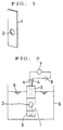
- Fig. 1 is a perspective view of a plate made of an ABS resin used as a jig for carrying out the migration test to accomplish the present invention.
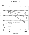
- Fig. 2 is an illustrative side view of an apparatus for carrying out the migration test to accomplish the present invention.
- Fig. 3 is a perspective view of an example of the female terminal of the present invention made by way of trial for testing its performance.
- Fig. 4 is a perspective view of another example of the female terminal of the present invention made by way of trial for testing its performance.
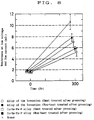
- Fig. 5 is a graph showing the relationship between the contact load and the conditions for heat treatment in the case of measuring the stress relaxation characteristics of the copper base alloy for terminals of the present invention.
- Fig. 6 is a graph showing the relationship between the contact load and the conditions for heat treatment in the case of measuring the stress relaxation characteristics of the copper base alloy for terminals of the present invention.
- Fig. 7 is a graph showing the results of measurement of resistance at low voltage and low current in the tests of electrical performance of the copper base alloy for terminals of the present invention.
- Fig. 8 is a graph showing the results of measurement of resistance at low voltage and low current in the tests of electrical performance of the copper base alloy for terminals of the present invention.
- the present invention provides a copper base alloy for terminals that consists essentially, on a weight basis, of 0.5 - 3.0 % Ni, 0.5 - 2.0 % Sn, 0.010 - 0.20 % P and the balance of Cu and incidental impurities.
- the present invention provides a copper base alloy for terminals that consists essentially, on a weight basis, of 0.5 - 3.0 % Ni, 0.5 - 2.0 % Sn, 0.010 - 0.20 % P and the balance of Cu and incidental impurities, with the ratio of Ni to P (Ni/P) being in the range of 10 - 50 and fine precipitates of Ni-P compound in the size of no larger than 100 nm being uniformly dispersed in the alloy.
- the present invention provides a copper base alloy for terminals that consists essentially, on a weight basis, of 0.5 - 3.0 % Ni, 0.5 - 2.0 % Sn, 0.010 - 0.20 % P and the balance of Cu and incidental impurities, with the ratio of Ni to P (Ni/P) being in the range of 10 - 50 and fine precipitates of Ni-P compound in the size of no larger than 100 nm being uniformly dispersed in the alloy, said alloy having a tensile strength of at least 500 N/mm 2 .
- a spring limit of at least 400 N/mm 2 a stress relaxation of no more than 10%, a conductivity of at least 30 % IACS and a bending workability given in terms of the ratio of R to t (R/t) of no more than 2, where R is a bend radius and t is a thickness of the specimen.
- the present invention provides a copper base alloy for terminals that consists essentially, on a weight basis, of 0.5 - 3.0 % Ni, 0.5 - 2.0 % Sn, 0.010 - 0.20 % P and 0.01 - 2.0 % Zn and the balance of Cu and incidental impurities.
- the present invention provides a copper base alloy for terminals that consists essentially, on a weight basis, of 0.5 - 3.0 % Ni, 0.5 - 2.0 % Sn, 0.010 - 0.20 % P, 0.01 - 2.0 % Zn and the balance of Cu and incidental impurities, with the ratio of Ni to P (Ni/P) being in the range of 10 - 50, fine precipitates of Ni-P compound in the size of no larger than 100 nm being uniformly dispersed in the alloy.
- the present invention provides a copper base alloy for terminals that consists essentially, on a weight basis, of 0.5 - 3.0 % Ni, 0.5 - 2.0 % Sn, 0.010 - 0.20 % P, 0.01 - 2.0 % Zn and the balance of Cu and incidental impurities, with the ratio of Ni to P (Ni/P) being in the range of 10 - 50, fine precipitates of Ni-P compound in the size of no larger than 10 nm being uniformly dispersed in the alloy, said alloy having a tensile strength of at least 500 N/mm 2 , a sprig limit of at least 400 N/mm 2 , a stress relaxation of no more than 10%, a conductivity of at least 30 % IACS and a bending workability given in terms of the ratio of R to t (R/t) of no more than 2, where R is a bend radius and t is a thickness of the specimen.
- the present invention provides a terminal with a built-in spring that is produced from a spring material or a terminal that is entirely made of said spring material including a spring as an integral part, said spring material being produced by melting a copper base alloy that consists essentially, on a weight basis, of 0.5 - 3.0 % Ni, 0.5 - 2.0 % Sn, 0.010 - 0.20 % P and the balance of Cu and incidental impurities, said alloy being worked, after melting, by hot- and cold- rolling.
- the present invention provides a terminal with a built-in spring that is produced from a spring material or a terminal that is entirely made of said spring material including a spring as an integral part, said spring material being produced by melting a copper base alloy that consists essentially, on a weight basis, of 0.5 - 3.0 % Ni, 0.5 - 2.0 % Sn, 0.010 - 0.20 % P and the balance of Cu and incidental impurities, with the ratio of Ni to P (Ni/P) being in the range of 10 - 50, fine precipitates of Ni-P compound within the size of no larger than 10 nm being uniformly dispersed in the alloy, said alloy being worked, after melting, by at least one of cold rolling and hot rolling.
- the present invention provides a terminal with a built-in spring that is produced from a spring material or a terminal that is entirely made of said spring material including a spring as an integral part, said spring material being produced by melting a copper base alloy that consists essentially, on a weight basis, of 0.5 - 3.0 % Ni, 0.5 - 2.0 % Sn, 0.010 - 0.20 % P, 0.01 - 2.0 % Zn and the balance of Cu and incidental impurities, said alloy being worked, after melting, by at least one of cold rolling and hot rolling.
- the present invention provides a terminal with a built-in spring that is produced from a spring material or a terminal that is entirely made of said spring material including a spring as an integral part, said spring material being produced by melting a copper base alloy that consists essentially, on a weight basis, of 0.5 - 3.0 % Ni, 0.5 - 2.0 % Sn, 0.010 - 0.20 % P, 0.01 - 2.0 % Zn and the balance of Cu and incidental impurities, with a ratio of Ni to P (Ni/P) being in the range of 10 - 50, fine precipitates of Ni-P compound within the size of no larger than 100 nm being uniformly dispersed in the alloy, said alloy being worked, after melting, by at least one of cold rolling and hot rolling.
- a copper base alloy that consists essentially, on a weight basis, of 0.5 - 3.0 % Ni, 0.5 - 2.0 % Sn, 0.010 - 0.20 % P, 0.01 - 2.0 % Zn and the
- the present invention provides a terminal to be used as a connector terminal in automobiles and other applications, said terminal being one with a built-in spring that is produced from a spring material or a terminal that is entirely made of said spring material including a spring as an integral part, said spring material being produced by the method defined by any of the seventh through the tenth aspects given above.
- Nickel (Ni) dissolves in the Cu matrix to provide improved strength, elasticity, heat resistance, anti-stress relaxation, anti-migration and anti-stress corrosion cracking characteristics. Further, Ni forms a compound with P, which disperses and precipitates to provide higher conductivity. If the Ni content is less than 0.5%, the desired effects will not be achieved; if the Ni content exceeds 3.0%, its effects will be saturated and its economy will be impaired. Therefore, the Ni content is specified to range from 0.5 to 3.0 wt%.
- Tin (Sn) also dissolves in the Cu matrix to provide improved strength, elasticity and corrosion resistance. If the Sn content is less than0.5%, the desired effects will not be achieved with respect to the strength and elasticity,; if the Sn content exceeds 2.0%, its effects will be saturated. Therefore, the Sn content is specified to range from 0.5 to 2.0 wt%.
- Phosphorus (P) not only works as a deoxidizer of the melt but also forms a compound with Ni, which disperses and precipitates to improve not only conductivity but also strength, elasticity, and anti-stress relaxation characteristics. If the P content is less than 0.005%, the desired effects will not be achieved; if the P content exceeds 0.20%, the conductivity, workability and adhesive quality of soldering or plating after the heat treatment thereof will be severely impaired even in the copresence of Ni, as well as anti-migration characteristics will be decreased. Therefore, the P content is specified to range from 0.010 to 0.2 wt%, preferably from 0.02 to 0.15 wt%.
- the ratio of weight percentages of Ni to P should preferably be limited within a specified range; preferably in the range of from 10 to 50; more preferably in the range of from 15 to 30. If the size of precipitated Ni-P compound exceeds 100 nm, contribution of the precipitate to the improvement in strength, elasticity and anti-stress relaxation characteristics and the bending workability will be impaired.
- the life of a metal mold for pressing which comprises a punch made of a hard alloy and a die made of a tool steel, often decreases if the alloy structure contains a large amount of Ni-P precipitate whose size exceeds 100 nm. Therefore, the size of Ni-P precipitate is specified to be 100 nm or less, more preferably 70 nm or less.
- zinc (Zn) which can be added as an auxiliary component, has the ability to further improve the adhesive quality of a plating layer to the surface of a copper base alloy, when heat treated after plating.
- Zn content is up to 0.01%, the above-mentioned effects will not be achieved; if the Zn content exceeds 2.0%, its effects will be saturated. Therefore, the Zn content within the range of 0.01 - 2.0 wt% is preferred.
- insertion force and extraction force herein used for connector terminals represent, respectively, the “force required to insert a male terminal into a female terminal” and the “force required to break the male terminal away from the female terminal”.
- the insertion force should preferably be small and the extraction force should preferably be large. If the insertion force is unduly large, the male terminal cannot be readily inserted into the female terminal. This causes a particular problem with circuits of high packing density because routine assembling operations cannot be accomplished efficiently if the number of terminals to be connected increases. On the other hand, if the extraction force is too weak, separation occurs due to the vibration or an oxide film will easily form and the contact resistance is too unstable to insure satisfactory electrical reliability for connectors.
- the initial insertion/extraction force of the terminal is desirably from 1.5N to 30N and, to this end, the terminal material to be used must have a tensile strength of at least 500 N/mm 2 , a spring limit of at least 400 N/mm 2 and, from a view point of good moldability of terminals, a value of R/t of 2 or less.
- the crystal grain size is 50 ⁇ m or less, more preferably 25 ⁇ m or less.
- the initial resistance at low voltage and low current is desirably small, preferably not more than 3 m ⁇ .
- the value of contact electric resistance is dependent primarily on how much the contact load on the coupling will decrease due to heat cycles. However, the stress relaxation caused by spontaneous heat generation from the material as well as the stress relaxation caused by the effects of temperature in the automobile's engine room or around the exhaust system will also reduce the contact load, which eventually leads to a higher contact electric resistance.
- the terminal material itself must not undergo stress relaxation greater than 10% upon standing at 150°C for 1,000 hours, and it is also required to have a tensile strength of at least 500 N/mm 2 , a spring limit of at least 400 N/mm 2 , an electric conductivity of at least 30 % IACS and a stress relaxation after working into a spring of no more than 20%.
- Alloys having the compositions shown in Table 1 were melted in a high-frequency melting furnace and hot-rolled at 850°C, after heating to this temperature, to a thickness of 5.0 mm. Then, each sheet was subjected to facing to a thickness of 4.8 mm and by subsequent repitition of cold-rolling and heat treatment, sheets having a thickness of 0.2 mm were obtained at a final reduction ratio of 67%.
- the bending axis was set to be parallel to the rolling direction.
- stress relaxation(%) ⁇ (L 1 -L 2 )/(L 1 -L 0 ) ⁇ X100
- the migration test was conducted in the following way: A plate as shown in Fig. 1 (1: ABS resin; 2: opening) made of ABS resin (2 mm(t) X 16 mm(w) X 72 mm(l)) and having in the central area thereof a circular opening was sandwiched by a pair of test pieces (each 0.2 mm(t) X 5 mm(w) X 80 mm(l)) and the resulting assembly was joined together by winding around it at both upper and lower portions with separate pieces of Teflon tape. Then, the fixed assembly was held in a testing vessel filled with tap water as shown in Fig. 2 (3: Teflon tape; 4: test piece; 5: tap water; 6: testing vessel; 7: ammeter; 8: DC power source). The migration characteristics of each test piece was evaluated by measuring maximum leakage current after 8 hours' application of 14 V DC voltage.
- the alloy sample Nos. 1 - 8 prepared in accordance with the present invention had a tensile strength of at least 500 N/mm 2 , a spring limit of at least 400 N/mm 2 and a conductivity of at least 30 % IACS and their bending workability was also satisfactory.
- those samples had superior anti-stress relaxation characteristics represented by having a stress relaxation of not greater than 10% and also had superior anti-migration characteristics. It can therefore be concluded that the copper base alloys of the present invention are very advantageous for use in terminals in automobiles and other applications.
- the alloy sample Nos. 9 - 11 are comparison alloys made, respectively, of phosphor bronze, brass and Cu-Sn-Fe-P alloy.
- the alloys prepared in accordance with present invention were press formed into female terminals shown by 9 in Fig. 3, each being equipped with a spring 10.
- the terminals were subjected to a post-heat treatment in order to provide a good spring property.
- the heat treatment consisted of heating at 180°C for 30 minutes in order to prevent excessive surface deterioration so that Sn plating could subsequently be performed as a surface treatment of terminals.
- the so treated terminals were subjected to a test for evaluating their stress relaxation characteristics.
- female terminals made from a Cu-Sn-Fe-P alloy and a brass material were also subjected to a heat treatment under the same conditions and, thereafter, a performance test was conducted in the same manner.
- the terminals had an initial insertion force ranging from 4.5 to 6.0N and their initial resistance at low voltage and low current ranged from 1.5 to 2.0 m ⁇ .
- the female terminal made of the prior art Cu-Sn-Fe-P alloy experienced a greater drop in contact load than the female terminal made of the copper base alloy of the present invention and the stress relaxation of the former terminal was ca. 30%.
- the brass terminal experienced ca. 50% stress relaxation.
- the stress relaxation of the female terminal made of the copper base alloy within the scope of the present invention was ca. 12%, which satisfied the requirement for the stress relaxation of no more than 20% and hence was superior to the comparative terminals. Further, as shown in Fig. 6, the superiority of the terminals made of the alloy of the present invention was found to increase by subjecting the alloy to the heat treatment after press working.
- the copper base alloy of the present invention was also superior to the conventional Cu-Sn-Fe-P alloy and brass in terms of electrical performance. Also, as shown in Fig. 8, the superiority of the alloy of the present invention was found to be further improved by subjecting the alloy to the heat treatment after the press working thereof.
- Female terminals shown by 9 in Fig. 4 were shaped that had a built-in spring 10 made from the copper base alloy of the present invention.
- the terminals were subjected to the same tests as in the case of the terminals depicted in Fig. 3 and the test results were as well as in the case of the terminals shown in Fig. 3.
- Alloys having the compositions shown in Table 3 were melted in a high-frequency melting furnace and hot-rolled at 850°C to a thickness of 5.0 mm.
- the surface of each slab was scalped to a thickness of 4.8 mm and by subsequent repetition of cold-rolling operations and heat treatments, sheets having a thickness of 0.2 mm were obtained at the final reduction ratio of 67%.
- the alloy sample Nos. 12 - 19 prepared in accordance with the present invention had a tensile strength of at least 500 N/mm 2 , a spring limit of at least 400 N/mm 2 , and a conductivity of at least 30 % IACS, and their bending workability was also satisfactory.
- those samples had superior stress relaxation characteristics as given by a stress relaxation ratio of not greater than 10% as well as superior anti-migration characteristics.
- the comparison alloy sample No. 20 whose P content is lower and whose Ni/P ratio is larger than the alloy of the present invention, is inferior to the alloy of the present invention in tensile strength, spring limit, and stress relaxation characteristics. It is considered that this is because the P content and the Ni/P ratio of the comparison alloy are out of the suitable ranges defined in the present invention, and therefore, tensile strength, elasticity and anti-stress relaxation characteristics are unduly low.
- Additional disadvantages encountered in the production process include poor fluidity of the melt during the step of casting and not a small number of "rough surface” occurrances on the surface of an ingot.
- the production cost would increase.
- no less than 0.5% of Ni should be contained together with an appropriate amount of P and Sn.
- Comparison alloy sample No. 23 which contains less Ni and less P than the alloy of the present invention and which has a larger value of the Ni to P ratio (NI/P) is inferior to the alloy of the present invention, due to the less Ni content, in tensile strength, elasticity, anti-stress relaxation and anti-migration characteristics.
- the alloy should contain no less than 0.5% of Ni and no less than 0.005% of P together with a proper amount of Sn.
- Comparison alloy sample No. 25 which contains more Ni than the alloy of the present invention, is inferior in conductivity and bending workability.
- the addition of Ni in an amount more than a proper amount will merely increase the amount of Ni which dissolves in the Cu matrix to result in the decrease in electric conductivity as well as the decrease in bending workability.
- Comparison alloy sample No. 26 which contains less Sn than the alloy of the present invention, is inferior in tensile strength and elasticity. If the Sn content is less than the amount defined in the present invention, satisfactory characteristics will not be obtained with respect to tensile strength and elasticity even if the contents of Ni and P are appropriate and the value of the Ni/P ratio is proper.
- Alloys having the compositions shown in Table 4 were melted in a high-frequency melting furnace and hot-rolled at 850°C to a thickness of 5.0 mm.
- the surface of each slab was scalped to a thickness of 4.8 mm and by subsequent repetition of cold-rolling operations and heat treatments, sheets having a thickness of 0.2 mm with a final reduction ratio of 67% were obtained.
- conditions of heat treatments (age-precipitation) were varied in order to vary the sizes of precipitates and the crystal grain diameters thereof.
- precipitates an average diameter of the largest 10 precipitate particles determined by transmission electron microscopy, wherein the specimen being observed at three phases at the magnification of 50,000X, was shown as the size of the precipitate. Crystal grain diameters were evaluated according to JIS H 0501.
- all the alloy sample Nos. 27 - 34 prepared in accordance with the present invention had a tensile strength of no less than 500 N/mm 2 , a spring limit of no less than 400 N/mm 2 and a conductivity of no less than 30% IACS, and their bending workability was also satisfactory.
- these samples had superior stress relaxation characteristics of no less than 10% as well as superior anti-migration characteristics.
- the copper base alloy of the present invention for use in terminals is superior in tensile strength, spring limit, electric conductivity, anti-stress relaxation characteristics, anti-migration characteristics and bending workability.
- a terminal which is constructed by the alloy of the present invention and which has a spring in it is superior in the resistance at low voltage and low current as well as stress relaxation characteristics, and therefore the alloy has a remarkable advantage from a view point of industry.
- a copper base alloy for use in a terminal which has an electric conductivity of as high as at least 30% IACS and also has both high tensile strength and high spring limit as well as superior stress relaxation characteristics of not higher than 10%.
- a terminal which has contained in its structure a spring made of the alloy of the present invention or a terminal wholly made of the alloy of the present invention inclusive of its spring, the terminal having proper initial properties inclusive of a proper insertion power in the range of 1.5 - 30 N, a proper resistance at low voltage and low current of no more than 3 m ⁇ and a proper stress relaxation characteristics of no more than 20%.
Landscapes
- Chemical & Material Sciences (AREA)
- Engineering & Computer Science (AREA)
- Materials Engineering (AREA)
- Mechanical Engineering (AREA)
- Metallurgy (AREA)
- Organic Chemistry (AREA)
- Physics & Mathematics (AREA)
- Thermal Sciences (AREA)
- Crystallography & Structural Chemistry (AREA)
- Conductive Materials (AREA)
Applications Claiming Priority (3)
| Application Number | Priority Date | Filing Date | Title |
|---|---|---|---|
| JP7259497 | 1997-02-18 | ||
| JP9072594A JPH10226835A (ja) | 1997-02-18 | 1997-02-18 | 端子用銅基合金とそれを用いた端子 |
| JP72594/97 | 1997-02-18 |
Publications (2)
| Publication Number | Publication Date |
|---|---|
| EP0859065A1 true EP0859065A1 (de) | 1998-08-19 |
| EP0859065B1 EP0859065B1 (de) | 2004-05-12 |
Family
ID=13493889
Family Applications (1)
| Application Number | Title | Priority Date | Filing Date |
|---|---|---|---|
| EP98102539A Expired - Lifetime EP0859065B1 (de) | 1997-02-18 | 1998-02-13 | Legierungen auf Kupferbasis sowie Anschlusselementen |
Country Status (4)
| Country | Link |
|---|---|
| EP (1) | EP0859065B1 (de) |
| JP (1) | JPH10226835A (de) |
| KR (1) | KR100357501B1 (de) |
| DE (1) | DE69823713T2 (de) |
Cited By (6)
| Publication number | Priority date | Publication date | Assignee | Title |
|---|---|---|---|---|
| US6471792B1 (en) | 1998-11-16 | 2002-10-29 | Olin Corporation | Stress relaxation resistant brass |
| EP1265342A3 (de) * | 2001-06-06 | 2006-02-01 | Mabuchi Motor Co., Ltd | Läufer eines Kleinmotors und Verfahren zur Herstellung desselben |
| EP1801249A1 (de) * | 2005-12-22 | 2007-06-27 | Kabushiki Kaisha Kobe Seiko Sho | Kupferlegierung mit exzellenten Spannungsrelaxationseigenschaften |
| EP2451604A4 (de) * | 2009-07-10 | 2013-04-10 | Luvata Espoo Oy | Kupferlegierung für ein wärmetauscherrohr |
| EP2184371A4 (de) * | 2007-08-07 | 2013-05-01 | Kobe Steel Ltd | Kupferlegierungsblech |
| EP3106546A4 (de) * | 2014-02-13 | 2017-06-28 | Kabushiki Kaisha Kobe Seiko Sho (Kobe Steel, Ltd.) | Kupferlegierungsblech mit oberflächenschicht mit hervorragender wärmebeständigkeit |
Families Citing this family (5)
| Publication number | Priority date | Publication date | Assignee | Title |
|---|---|---|---|---|
| JP4984108B2 (ja) * | 2005-09-30 | 2012-07-25 | Dowaメタルテック株式会社 | プレス打抜き性の良いCu−Ni−Sn−P系銅合金およびその製造法 |
| JP5243744B2 (ja) * | 2007-08-01 | 2013-07-24 | Dowaメタルテック株式会社 | コネクタ端子 |
| JP5466879B2 (ja) | 2009-05-19 | 2014-04-09 | Dowaメタルテック株式会社 | 銅合金板材およびその製造方法 |
| JP5436391B2 (ja) * | 2010-10-22 | 2014-03-05 | Dowaメタルテック株式会社 | 皮膜および電気電子部品 |
| JP6155405B2 (ja) | 2015-04-24 | 2017-06-28 | 古河電気工業株式会社 | 銅合金材料およびその製造方法 |
Citations (7)
| Publication number | Priority date | Publication date | Assignee | Title |
|---|---|---|---|---|
| JPS596346A (ja) * | 1982-07-05 | 1984-01-13 | Furukawa Electric Co Ltd:The | 半導体機器のリ−ド材用銅合金 |
| JPH01316432A (ja) * | 1988-06-16 | 1989-12-21 | Dowa Mining Co Ltd | ハンダ耐候性にすぐれた導電材料用銅合金 |
| JPH036341A (ja) * | 1989-06-02 | 1991-01-11 | Dowa Mining Co Ltd | 高強度高導電性銅基合金 |
| JPH04154942A (ja) * | 1990-10-17 | 1992-05-27 | Dowa Mining Co Ltd | コネクタ用銅基合金の製造法 |
| US5322575A (en) * | 1991-01-17 | 1994-06-21 | Dowa Mining Co., Ltd. | Process for production of copper base alloys and terminals using the same |
| US5387293A (en) * | 1991-01-17 | 1995-02-07 | Dowa Mining Co., Ltd. | Copper base alloys and terminals using the same |
| JPH07331363A (ja) * | 1994-06-01 | 1995-12-19 | Nikko Kinzoku Kk | 高力高導電性銅合金 |
-
1997
- 1997-02-18 JP JP9072594A patent/JPH10226835A/ja active Pending
-
1998
- 1998-02-13 DE DE69823713T patent/DE69823713T2/de not_active Expired - Lifetime
- 1998-02-13 EP EP98102539A patent/EP0859065B1/de not_active Expired - Lifetime
- 1998-02-17 KR KR1019980004793A patent/KR100357501B1/ko not_active Expired - Lifetime
Patent Citations (7)
| Publication number | Priority date | Publication date | Assignee | Title |
|---|---|---|---|---|
| JPS596346A (ja) * | 1982-07-05 | 1984-01-13 | Furukawa Electric Co Ltd:The | 半導体機器のリ−ド材用銅合金 |
| JPH01316432A (ja) * | 1988-06-16 | 1989-12-21 | Dowa Mining Co Ltd | ハンダ耐候性にすぐれた導電材料用銅合金 |
| JPH036341A (ja) * | 1989-06-02 | 1991-01-11 | Dowa Mining Co Ltd | 高強度高導電性銅基合金 |
| JPH04154942A (ja) * | 1990-10-17 | 1992-05-27 | Dowa Mining Co Ltd | コネクタ用銅基合金の製造法 |
| US5322575A (en) * | 1991-01-17 | 1994-06-21 | Dowa Mining Co., Ltd. | Process for production of copper base alloys and terminals using the same |
| US5387293A (en) * | 1991-01-17 | 1995-02-07 | Dowa Mining Co., Ltd. | Copper base alloys and terminals using the same |
| JPH07331363A (ja) * | 1994-06-01 | 1995-12-19 | Nikko Kinzoku Kk | 高力高導電性銅合金 |
Non-Patent Citations (5)
| Title |
|---|
| PATENT ABSTRACTS OF JAPAN vol. 008, no. 085 (C - 219) 18 April 1984 (1984-04-18) * |
| PATENT ABSTRACTS OF JAPAN vol. 014, no. 115 (C - 0696) 5 March 1990 (1990-03-05) * |
| PATENT ABSTRACTS OF JAPAN vol. 015, no. 123 (C - 0816) 26 March 1991 (1991-03-26) * |
| PATENT ABSTRACTS OF JAPAN vol. 016, no. 443 (C - 0985) 16 September 1992 (1992-09-16) * |
| PATENT ABSTRACTS OF JAPAN vol. 096, no. 004 30 April 1996 (1996-04-30) * |
Cited By (12)
| Publication number | Priority date | Publication date | Assignee | Title |
|---|---|---|---|---|
| US6471792B1 (en) | 1998-11-16 | 2002-10-29 | Olin Corporation | Stress relaxation resistant brass |
| EP1265342A3 (de) * | 2001-06-06 | 2006-02-01 | Mabuchi Motor Co., Ltd | Läufer eines Kleinmotors und Verfahren zur Herstellung desselben |
| EP1801249A1 (de) * | 2005-12-22 | 2007-06-27 | Kabushiki Kaisha Kobe Seiko Sho | Kupferlegierung mit exzellenten Spannungsrelaxationseigenschaften |
| US8641837B2 (en) | 2005-12-22 | 2014-02-04 | Kobe Steel, Ltd. | Copper alloy having excellent stress relaxation property |
| CN104046836A (zh) * | 2005-12-22 | 2014-09-17 | 株式会社神户制钢所 | 具有优异应力松弛性的铜合金 |
| CN104046836B (zh) * | 2005-12-22 | 2016-07-27 | 株式会社神户制钢所 | 具有优异应力松弛性的铜合金 |
| EP2184371A4 (de) * | 2007-08-07 | 2013-05-01 | Kobe Steel Ltd | Kupferlegierungsblech |
| EP2695957A3 (de) * | 2007-08-07 | 2014-07-02 | Kabushiki Kaisha Kobe Seiko Sho | Kupferlegierungsblech |
| EP2695958A3 (de) * | 2007-08-07 | 2014-07-02 | Kabushiki Kaisha Kobe Seiko Sho | Kupferlegierungsblech |
| EP2451604A4 (de) * | 2009-07-10 | 2013-04-10 | Luvata Espoo Oy | Kupferlegierung für ein wärmetauscherrohr |
| CN107739880A (zh) * | 2009-07-10 | 2018-02-27 | 鲁瓦塔富兰克林股份有限公司 | 用于热交换器管的铜合金 |
| EP3106546A4 (de) * | 2014-02-13 | 2017-06-28 | Kabushiki Kaisha Kobe Seiko Sho (Kobe Steel, Ltd.) | Kupferlegierungsblech mit oberflächenschicht mit hervorragender wärmebeständigkeit |
Also Published As
| Publication number | Publication date |
|---|---|
| DE69823713T2 (de) | 2005-04-28 |
| EP0859065B1 (de) | 2004-05-12 |
| DE69823713D1 (de) | 2004-06-17 |
| KR19980071423A (ko) | 1998-10-26 |
| KR100357501B1 (ko) | 2002-12-18 |
| JPH10226835A (ja) | 1998-08-25 |
Similar Documents
| Publication | Publication Date | Title |
|---|---|---|
| JP5191725B2 (ja) | Cu−Zn−Sn系銅合金板材およびその製造法並びにコネクタ | |
| JP3739214B2 (ja) | 電子部品用銅合金板 | |
| US5322575A (en) | Process for production of copper base alloys and terminals using the same | |
| US4599120A (en) | Processing of copper alloys | |
| CA1250157A (en) | Copper-beryllium-cobalt alloys | |
| JP2001526734A (ja) | 錫被覆電気コネクタ | |
| US6254702B1 (en) | Copper base alloys and terminals using the same | |
| KR100329153B1 (ko) | 단자 및 커넥터용 구리합금 및 그 제조방법 | |
| EP0859065B1 (de) | Legierungen auf Kupferbasis sowie Anschlusselementen | |
| EP2221391A1 (de) | Kupferlegierungsblechmaterial | |
| JP3717321B2 (ja) | 半導体リードフレーム用銅合金 | |
| JPH0533087A (ja) | 小型導電性部材用銅合金 | |
| JP2000355721A (ja) | 耐亀裂性が増強された銅合金 | |
| JP2000256814A (ja) | 端子用銅基合金条の製造方法 | |
| US4724013A (en) | Processing of copper alloys and product | |
| US5853505A (en) | Iron modified tin brass | |
| CA1249736A (en) | Processing of copper alloys | |
| EP0460454B1 (de) | Hochfeste Kupferlegierung mit ausgezeichneter Biegsamkeit für elektrische Stromleiter | |
| US5387293A (en) | Copper base alloys and terminals using the same | |
| DE60006195T2 (de) | Kupfer-Legierung für elektrische oder elektronische Bauteile | |
| CN114248038A (zh) | 无铅焊料组合物 | |
| JP3807475B2 (ja) | 端子・コネクタ用銅合金板及びその製造方法 | |
| JP2001214226A (ja) | 端子用銅基合金、該合金条および該合金条の製造方法 | |
| JP2000129377A (ja) | 端子用銅基合金 | |
| JPH04236736A (ja) | 端子用銅基合金 |
Legal Events
| Date | Code | Title | Description |
|---|---|---|---|
| PUAI | Public reference made under article 153(3) epc to a published international application that has entered the european phase |
Free format text: ORIGINAL CODE: 0009012 |
|
| AK | Designated contracting states |
Kind code of ref document: A1 Designated state(s): DE FI FR GB IT NL SE |
|
| AX | Request for extension of the european patent |
Free format text: AL;LT;LV;MK;RO;SI |
|
| 17P | Request for examination filed |
Effective date: 19990217 |
|
| AKX | Designation fees paid |
Free format text: DE FI FR GB IT NL SE |
|
| RBV | Designated contracting states (corrected) |
Designated state(s): DE FI FR GB IT NL SE |
|
| 17Q | First examination report despatched |
Effective date: 20000914 |
|
| GRAP | Despatch of communication of intention to grant a patent |
Free format text: ORIGINAL CODE: EPIDOSNIGR1 |
|
| GRAS | Grant fee paid |
Free format text: ORIGINAL CODE: EPIDOSNIGR3 |
|
| GRAA | (expected) grant |
Free format text: ORIGINAL CODE: 0009210 |
|
| AK | Designated contracting states |
Kind code of ref document: B1 Designated state(s): DE FI FR GB IT NL SE |
|
| REG | Reference to a national code |
Ref country code: GB Ref legal event code: FG4D |
|
| REF | Corresponds to: |
Ref document number: 69823713 Country of ref document: DE Date of ref document: 20040617 Kind code of ref document: P |
|
| REG | Reference to a national code |
Ref country code: SE Ref legal event code: TRGR |
|
| ET | Fr: translation filed | ||
| PLBE | No opposition filed within time limit |
Free format text: ORIGINAL CODE: 0009261 |
|
| STAA | Information on the status of an ep patent application or granted ep patent |
Free format text: STATUS: NO OPPOSITION FILED WITHIN TIME LIMIT |
|
| 26N | No opposition filed |
Effective date: 20050215 |
|
| REG | Reference to a national code |
Ref country code: FR Ref legal event code: PLFP Year of fee payment: 19 |
|
| REG | Reference to a national code |
Ref country code: FR Ref legal event code: PLFP Year of fee payment: 20 |
|
| PGFP | Annual fee paid to national office [announced via postgrant information from national office to epo] |
Ref country code: NL Payment date: 20170110 Year of fee payment: 20 |
|
| PGFP | Annual fee paid to national office [announced via postgrant information from national office to epo] |
Ref country code: FR Payment date: 20170112 Year of fee payment: 20 Ref country code: SE Payment date: 20170213 Year of fee payment: 20 Ref country code: DE Payment date: 20170207 Year of fee payment: 20 Ref country code: FI Payment date: 20170209 Year of fee payment: 20 |
|
| PGFP | Annual fee paid to national office [announced via postgrant information from national office to epo] |
Ref country code: GB Payment date: 20170208 Year of fee payment: 20 |
|
| PGFP | Annual fee paid to national office [announced via postgrant information from national office to epo] |
Ref country code: IT Payment date: 20170221 Year of fee payment: 20 |
|
| REG | Reference to a national code |
Ref country code: DE Ref legal event code: R071 Ref document number: 69823713 Country of ref document: DE |
|
| REG | Reference to a national code |
Ref country code: NL Ref legal event code: MK Effective date: 20180212 |
|
| REG | Reference to a national code |
Ref country code: GB Ref legal event code: PE20 Expiry date: 20180212 |
|
| PG25 | Lapsed in a contracting state [announced via postgrant information from national office to epo] |
Ref country code: GB Free format text: LAPSE BECAUSE OF EXPIRATION OF PROTECTION Effective date: 20180212 |