EP0859264B1 - Modulateur acousto-optique comprenant un guide d'onde optique - Google Patents
Modulateur acousto-optique comprenant un guide d'onde optique Download PDFInfo
- Publication number
- EP0859264B1 EP0859264B1 EP98300559A EP98300559A EP0859264B1 EP 0859264 B1 EP0859264 B1 EP 0859264B1 EP 98300559 A EP98300559 A EP 98300559A EP 98300559 A EP98300559 A EP 98300559A EP 0859264 B1 EP0859264 B1 EP 0859264B1
- Authority
- EP
- European Patent Office
- Prior art keywords
- substrate
- waveguide
- solder composition
- solder
- optical fiber
- Prior art date
- Legal status (The legal status is an assumption and is not a legal conclusion. Google has not performed a legal analysis and makes no representation as to the accuracy of the status listed.)
- Expired - Lifetime
Links
- 230000003287 optical effect Effects 0.000 title claims description 33
- 239000000758 substrate Substances 0.000 claims description 74
- 239000013307 optical fiber Substances 0.000 claims description 67
- 229910000679 solder Inorganic materials 0.000 claims description 61
- 239000000203 mixture Substances 0.000 claims description 41
- 230000001902 propagating effect Effects 0.000 claims description 16
- 229910052738 indium Inorganic materials 0.000 claims description 10
- APFVFJFRJDLVQX-UHFFFAOYSA-N indium atom Chemical compound [In] APFVFJFRJDLVQX-UHFFFAOYSA-N 0.000 claims description 8
- 229910003327 LiNbO3 Inorganic materials 0.000 claims description 7
- VYPSYNLAJGMNEJ-UHFFFAOYSA-N Silicium dioxide Chemical compound O=[Si]=O VYPSYNLAJGMNEJ-UHFFFAOYSA-N 0.000 claims description 5
- 230000008878 coupling Effects 0.000 claims description 4
- 238000010168 coupling process Methods 0.000 claims description 4
- 238000005859 coupling reaction Methods 0.000 claims description 4
- 230000000704 physical effect Effects 0.000 claims description 2
- 229910052681 coesite Inorganic materials 0.000 claims 2
- 229910052906 cristobalite Inorganic materials 0.000 claims 2
- 239000000377 silicon dioxide Substances 0.000 claims 2
- 229910052682 stishovite Inorganic materials 0.000 claims 2
- 229910052905 tridymite Inorganic materials 0.000 claims 2
- 230000000063 preceeding effect Effects 0.000 claims 1
- 239000000835 fiber Substances 0.000 description 24
- 239000000463 material Substances 0.000 description 18
- XLOMVQKBTHCTTD-UHFFFAOYSA-N Zinc monoxide Chemical compound [Zn]=O XLOMVQKBTHCTTD-UHFFFAOYSA-N 0.000 description 13
- 230000005540 biological transmission Effects 0.000 description 7
- 230000000694 effects Effects 0.000 description 6
- 238000000034 method Methods 0.000 description 6
- 239000011787 zinc oxide Substances 0.000 description 6
- 239000011248 coating agent Substances 0.000 description 4
- 238000000576 coating method Methods 0.000 description 4
- 230000001419 dependent effect Effects 0.000 description 3
- 239000011521 glass Substances 0.000 description 3
- 230000000644 propagated effect Effects 0.000 description 3
- 235000003913 Coccoloba uvifera Nutrition 0.000 description 2
- 240000008976 Pterocarpus marsupium Species 0.000 description 2
- 238000004891 communication Methods 0.000 description 2
- 238000004519 manufacturing process Methods 0.000 description 2
- 230000004048 modification Effects 0.000 description 2
- 238000012986 modification Methods 0.000 description 2
- 239000002245 particle Substances 0.000 description 2
- 238000000926 separation method Methods 0.000 description 2
- JBRZTFJDHDCESZ-UHFFFAOYSA-N AsGa Chemical compound [As]#[Ga] JBRZTFJDHDCESZ-UHFFFAOYSA-N 0.000 description 1
- RYGMFSIKBFXOCR-UHFFFAOYSA-N Copper Chemical compound [Cu] RYGMFSIKBFXOCR-UHFFFAOYSA-N 0.000 description 1
- 239000004593 Epoxy Substances 0.000 description 1
- 229910001218 Gallium arsenide Inorganic materials 0.000 description 1
- BQCADISMDOOEFD-UHFFFAOYSA-N Silver Chemical compound [Ag] BQCADISMDOOEFD-UHFFFAOYSA-N 0.000 description 1
- RTAQQCXQSZGOHL-UHFFFAOYSA-N Titanium Chemical compound [Ti] RTAQQCXQSZGOHL-UHFFFAOYSA-N 0.000 description 1
- NIXOWILDQLNWCW-UHFFFAOYSA-N acrylic acid group Chemical group C(C=C)(=O)O NIXOWILDQLNWCW-UHFFFAOYSA-N 0.000 description 1
- 239000000654 additive Substances 0.000 description 1
- 238000004026 adhesive bonding Methods 0.000 description 1
- 238000005253 cladding Methods 0.000 description 1
- 229910052802 copper Inorganic materials 0.000 description 1
- 239000010949 copper Substances 0.000 description 1
- 239000013078 crystal Substances 0.000 description 1
- 230000005489 elastic deformation Effects 0.000 description 1
- 230000005284 excitation Effects 0.000 description 1
- PCHJSUWPFVWCPO-UHFFFAOYSA-N gold Chemical compound [Au] PCHJSUWPFVWCPO-UHFFFAOYSA-N 0.000 description 1
- 229910052737 gold Inorganic materials 0.000 description 1
- 239000010931 gold Substances 0.000 description 1
- 238000009434 installation Methods 0.000 description 1
- 230000003993 interaction Effects 0.000 description 1
- 239000011133 lead Substances 0.000 description 1
- 239000005355 lead glass Substances 0.000 description 1
- GQYHUHYESMUTHG-UHFFFAOYSA-N lithium niobate Chemical compound [Li+].[O-][Nb](=O)=O GQYHUHYESMUTHG-UHFFFAOYSA-N 0.000 description 1
- 238000010895 photoacoustic effect Methods 0.000 description 1
- 238000012545 processing Methods 0.000 description 1
- 230000001681 protective effect Effects 0.000 description 1
- 230000000452 restraining effect Effects 0.000 description 1
- 229910052710 silicon Inorganic materials 0.000 description 1
- 239000010703 silicon Substances 0.000 description 1
- 229910052709 silver Inorganic materials 0.000 description 1
- 239000004332 silver Substances 0.000 description 1
- 239000011343 solid material Substances 0.000 description 1
- 239000010936 titanium Substances 0.000 description 1
- 229910052719 titanium Inorganic materials 0.000 description 1
- 238000012546 transfer Methods 0.000 description 1
- 230000007704 transition Effects 0.000 description 1
Images

Classifications
-
- G—PHYSICS
- G02—OPTICS
- G02F—OPTICAL DEVICES OR ARRANGEMENTS FOR THE CONTROL OF LIGHT BY MODIFICATION OF THE OPTICAL PROPERTIES OF THE MEDIA OF THE ELEMENTS INVOLVED THEREIN; NON-LINEAR OPTICS; FREQUENCY-CHANGING OF LIGHT; OPTICAL LOGIC ELEMENTS; OPTICAL ANALOGUE/DIGITAL CONVERTERS
- G02F1/00—Devices or arrangements for the control of the intensity, colour, phase, polarisation or direction of light arriving from an independent light source, e.g. switching, gating or modulating; Non-linear optics
- G02F1/01—Devices or arrangements for the control of the intensity, colour, phase, polarisation or direction of light arriving from an independent light source, e.g. switching, gating or modulating; Non-linear optics for the control of the intensity, phase, polarisation or colour
- G02F1/0128—Devices or arrangements for the control of the intensity, colour, phase, polarisation or direction of light arriving from an independent light source, e.g. switching, gating or modulating; Non-linear optics for the control of the intensity, phase, polarisation or colour based on electro-mechanical, magneto-mechanical, elasto-optic effects
- G02F1/0131—Devices or arrangements for the control of the intensity, colour, phase, polarisation or direction of light arriving from an independent light source, e.g. switching, gating or modulating; Non-linear optics for the control of the intensity, phase, polarisation or colour based on electro-mechanical, magneto-mechanical, elasto-optic effects based on photo-elastic effects, e.g. mechanically induced birefringence
- G02F1/0134—Devices or arrangements for the control of the intensity, colour, phase, polarisation or direction of light arriving from an independent light source, e.g. switching, gating or modulating; Non-linear optics for the control of the intensity, phase, polarisation or colour based on electro-mechanical, magneto-mechanical, elasto-optic effects based on photo-elastic effects, e.g. mechanically induced birefringence in optical waveguides
-
- G—PHYSICS
- G02—OPTICS
- G02B—OPTICAL ELEMENTS, SYSTEMS OR APPARATUS
- G02B6/00—Light guides; Structural details of arrangements comprising light guides and other optical elements, e.g. couplings
- G02B6/24—Coupling light guides
- G02B6/36—Mechanical coupling means
- G02B6/3628—Mechanical coupling means for mounting fibres to supporting carriers
-
- G—PHYSICS
- G02—OPTICS
- G02B—OPTICAL ELEMENTS, SYSTEMS OR APPARATUS
- G02B6/00—Light guides; Structural details of arrangements comprising light guides and other optical elements, e.g. couplings
- G02B6/24—Coupling light guides
- G02B6/36—Mechanical coupling means
- G02B6/3628—Mechanical coupling means for mounting fibres to supporting carriers
- G02B6/3632—Mechanical coupling means for mounting fibres to supporting carriers characterised by the cross-sectional shape of the mechanical coupling means
- G02B6/3636—Mechanical coupling means for mounting fibres to supporting carriers characterised by the cross-sectional shape of the mechanical coupling means the mechanical coupling means being grooves
-
- G—PHYSICS
- G02—OPTICS
- G02B—OPTICAL ELEMENTS, SYSTEMS OR APPARATUS
- G02B6/00—Light guides; Structural details of arrangements comprising light guides and other optical elements, e.g. couplings
- G02B6/24—Coupling light guides
- G02B6/42—Coupling light guides with opto-electronic elements
- G02B6/4201—Packages, e.g. shape, construction, internal or external details
- G02B6/4219—Mechanical fixtures for holding or positioning the elements relative to each other in the couplings; Alignment methods for the elements, e.g. measuring or observing methods especially used therefor
- G02B6/4236—Fixing or mounting methods of the aligned elements
- G02B6/4238—Soldering
Definitions
- the invention relates to optical signal modulators.
- Optical transmission and processing systems are being implemented for use in various communication applications.
- telephone and data transmission systems are now in use that utilize optical fibers to transmit voice and data signals over long distances.
- data and/or digitized voice signals are modulated with an optical carrier signal for transmission.
- Modulation is the variation of a characteristic of a signal wave in accordance with a characteristic of another signal wave.
- FIG. 1 A modulator arrangement 500 according to this patent is illustrated in FIG. 1.
- the arrangement 500 includes an acoustic transducer 510 formed on a top surface 522 of a glass substrate 520.
- a bottom surface 524 of the substrate 520 has a precision-formed groove 540 with an exact radius. This groove radius is precisely formed to provide a Hertzian contact between an optical fiber 530 and the substrate groove 540, when the fiber 530 is pressed into the groove 540.
- a Hertzian contact results when two rigid bodies are forced together into a point or line contact.
- the stress in the region of the resulting contact causes elastic deformations proximate the groove 540 bringing the bodies 520 and 530 into hard contact with no gaps.
- a Hertzian contact enables propagation of acoustic or standing waves over an acoustic path formed entirely of solid material from the substrate 520 through the Hertzian contact interface and into the waveguide 530.
- acoustic waves generated by the transducer 510 propagate into the substrate 520, through the formed Hertzian contact, and into the optical fiber 530. These acoustic waves then interact and modulate an optical signal propagating in a core of the optical fiber 540 by an acousto-optic effect. If the substrate surface 522 is parallel to the substrate groove 540 such that acoustic waves strike the fiber 530 in a perpendicular manner, then a propagating light signal in the fiber 530 is phase modulated. However, if the surface 522 is at non-zero angle ⁇ relative to the length of the fiber 530, then generated acoustic waves would strike the fiber 530 at an angle of incidence (90°- ⁇ ). At particular incidence angles ⁇ , it is possible to produce an intensity modulation of the light signal propagating in the optical fiber by an acousto-optic effect.
- the Kino et. al. patent provides a non-invasive method of modulating signals in an optical fiber
- fabrication cost of the substrate and the required precision in forming the groove is undesirably high.
- US-A-4,735,485 discloses an acousto-optic frequency shifter having an optical fiber attached to an acoustic transducer.
- the device includes an optical fiber affixed, e.g., by epoxy gluing or indium bonding, to the surface of a base block upon which a transducer is formed.
- EP-A-0 591 540 discloses an external modulator for optical communications including a substrate with a transducer on one side and an optical fiber arranged on the other side.
- the optical fiber is attached to the surface of the substrate using a material having an acoustic impedance close to the acoustic impedance of the optical fiber cladding.
- US-A-3,653,743 discloses an electro-optic device with suppressed acousto-optic effects.
- the reference discloses that indium is useful material for acoustic energy coupling between, e.g., a gold-plated crystal such as gallium arsenide and lead, lead glass or titanium.
- the invention is an acousto-optic modulator arrangement with an optical waveguide coupled to a substrate having an acoustic transducer formed thereon, by an acoustically-compatible solder.
- An acoustically-compatible solder provides advantageously low power reflections at the substrate-solder and solder-optical waveguide interfaces for acoustic waves generated by the transducer. Such propagated acoustic waves are then useable to modulate a light signal propagating in the waveguide by an acousto-optic effect.
- an acoustically-compatible solder composition has a density ⁇ s and a physical property of enabling an acoustic wave to propagate within such composition at a certain velocity v s that produces a desired density-acoustic wave velocity product ⁇ s •v s .
- a desired density-acoustic wave velocity product ⁇ s •v s is a value relative to corresponding density-acoustic wave velocity product values for the materials of the substrate and optical waveguide to enable acoustic waves generated by the transducer to propagate through the substrate and solder composition, and into the waveguide with sufficiently low power reflections to achieve a desired propagation efficiency. Smaller differences between such product values of the substrate, solder and waveguide materials result in lower power reflections at the material interfaces and lower propagation losses.
- solder composition enables fabrication of a modulator at relatively low cost and complexity compared to the difficult to form precision grooves and Hertzian contacts of the Kino et al. patent. Furthermore, in addition to providing a propagation medium for acoustic waves directed at the waveguide, it is also possible for the acoustically-compatible solder to advantageously provide mechanical attachment of the waveguide to the substrate.
- solder of the modulator with a surface shape that reflects and focuses acoustic waves propagating from the substrate at the optical waveguide. In such a manner, a desirable increase in the acoustic wave energy reaching the optical waveguide is achievable.
- An acousto-optic modulator arrangement includes an optical waveguide, such as an optical fiber, coupled to a substrate having an acoustic transducer using an acoustically-compatible solder composition.
- an optical waveguide such as an optical fiber
- a substrate having an acoustic transducer using an acoustically-compatible solder composition.
- acoustic waves generated by the transducer propagate through the substrate and solder composition and into the waveguide to modulate an optical signal propagating therein by an opto-acoustic effect.
- acoustic wave refers to an elastic nonelectromagnetic wave having a frequency typically in the range from below one hertz up to tens of gigahertz.
- An elastic wave is a wave propagated in a medium having inertia and elasticity (the existence of forces which tend to restore any part of a medium to its original position), and in which displaced particles transfer momentum to adjoining particles and are themselves restored to their original position.
- An acoustically-compatible solder is a composition possessing a density ⁇ s and an ability to propagate an acoustic wave at a velocity v s that produces a desired density-acoustic wave velocity product ⁇ s •v s .
- the density-acoustic wave velocity product for a material will be generally referred to as the ⁇ •v product for that material.
- a desired ⁇ s •v s product for the solder composition is a value relative to ⁇ •v products of the corresponding substrate and optical waveguide materials to enable acoustic waves generated by the transducer to propagate through the substrate and solder, and into the waveguide with desirably low power reflections at the substrate-solder and solder-waveguide interfaces. Smaller differences between the ⁇ •v products of the respective materials result in lower power reflections at the interfaces and lower propagation losses. As a consequence, the materials for the solder, substrate and waveguide are selected with numerically close ⁇ •v products for providing sufficiently low power reflections to achieve desired propagation and modulation efficiencies.
- FIGS. 2 to 7 Several different exemplary acousto-optic modulator configurations according to the invention are described below with regard to FIGS. 2 to 7. Such exemplary arrangements are for illustration purposes only and not intended to be a limitation of the invention. It is should be readily understood that numerous other modulator configurations, whether employing different acoustically-compatible solders or otherwise, can also be fabricated in accordance with the invention.
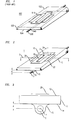
- FIG. 2 is a perspective view of the modulator 1 and FIG. 3 illustrates a cut-away view of the modulator 1 taken along reference line 3 of FIG. 2.
- the modulator 1 includes a section of an acoustic waveguide, such as an optical fiber 5, coupled to a surface 14 of a substrate 10 by an acoustically-compatible solder composition 15.
- a core 7 of the optical fiber 5 is also depicted.
- the substrate 10 is formed of a material which permits the transmission of acoustic waves therein. Suitable substrate materials include, for example, silica (SiO 2 ) glass and lithium niobate (LiNbO 3 ).
- a transducer 20 is formed on a surface 12 of the substrate 10 to launch acoustic waves through the substrate 10 in a direction of the optical fiber 5.
- the substrate surface 12 is at an angle ⁇ relative to the optical fiber 5.
- the optical fiber 5 is located at a distance d from the substrate 10 as shown in FIG. 3. Any protective optical fiber cover, such as an acrylic cover of conventional optical fibers, must be removed from the section of the optical fiber 5 coupled to the substrate 10.
- optical fiber 5 it is advantageous to align the optical fiber 5 relative to the transducer 20 such that, during operation, generated acoustic waves are directed at the optical fiber 5.
- Numerous techniques are useable to facilitate such alignment including, for example, providing alignment marks, notches or grooves on the substrate 10 to provide an alignment reference when attaching the optical fiber 5.
- the particular type of transducer used for the transducer 20 is not critical to practicing the invention as long as the transducer is capable of launching acoustic waves in the substrate 10 at the desired intensity and frequency.
- An exemplary transducer 20 is a zinc oxide (ZnO) transducer as depicted in FIG. 2.
- the ZnO transducer 20 includes a bottom electrode 22, such as copper or gold, a sputtered film 24 of ZnO having an exemplary thickness in the range of 2 ⁇ m to 5 ⁇ m, and a top electrode 26.
- the dimensions of the respective transducer electrode and film layers are dependent on the particular modulator application.
- An exemplary dimension for the bottom electrode in the approximate range of 1 to 2 cm long along the direction of the optical fiber 5.
- the widths of the bottom electrode 22 and ZnO film 24 should enable a sufficient bonding surface for electrical connection to the electrode 22.
- Exemplary dimensions for the top electrode 26 include a length of 10 mm and a width of 80 ⁇ m.
- a bond pad 28 for the top electrode 26 is provided to achieve the necessary electrical connection.
- Typical ZnO transducers can produce acoustic waves having frequencies in the range of 1 MHz to 1 GHz with a power typically in the range of 1 mW to 10 W. A more detailed description of ZnO transducers is provide in, for example, C. S. Tsai, Guided Wave Acousto-Optics - Interactions, Devices, and Applications, ch. 6, pp. 205-231 (Springer-Verlag, N.Y. 1990), which is incorporated
- the particular modulation performed by the acousto-optical modulator 1 is not critical to practicing the invention.
- the modulator 1 it is possible for the modulator 1 to perform phase or intensity modulation in the manner described in the previously cited Kino et al. patent, as well as Patterson et al., "Noninvasive Switchable Acousto-Optic Taps for Optical Fiber", J. of Lightwave Technol., vol. 9, no. 9, pp.1304-1312 (Sept. 1990), which is also incorporated by reference herein.
- the modulator 1 it is possible for the modulator 1 to provide intensity modulation of such an optical signal with a corresponding different angle ⁇ and with a single or multi-mode optical fiber 5.
- optical waveguide 5 A conventional optical fiber is depicted for the optical waveguide 5 for illustration purposes only.
- the particular type of optical waveguide 5 used is not critical to practicing the invention as long as such waveguides types facilitate the modulation of a light signal propagating therein by a acousto-optical effect.
- Alternative types of optical waveguides useable in accordance with the invention include, for example, waveguides fabricated in glass deposited on silicon.
- the solder 15 is formed of a composition having an advantageous ⁇ •v product relative to the ⁇ •v products of the substrate 10 and the optical fiber 5.
- the particular desired relationship of the ⁇ •v products for the selected composition is dependent on acceptable acoustic wave propagation losses at the optical fiber 5 relative to generated acoustic wave power by the transducer 20 to achieve a desired modulation efficiency.
- Such propagation losses are partially due to power reflections caused by acoustic property mismatches occurring at the respective interfaces between the substrate 10 and the solder 15, and the solder 15 and the optical fiber 5.
- smaller differences between the ⁇ •v products for the substrate, solder and waveguide materials produce smaller mismatches at the and correspondingly lower acoustic wave propagation losses at the optical fiber 5.
- An exemplary solder composition that is acoustically-compatible with a SiO 2 optical fiber 5 and SiO 2 or LiNbO 3 substrate 10 is a composition containing indium (In).
- Indium solders typical contain by weight 90% to 100% indium and 10% to 0% additives, such as silver (Ag).
- Typical values of densities ⁇ , acoustic wave velocities v and corresponding ⁇ •v products for SiO 2 , LiNbO 3 and solder composition of substantially 100% In by weight are listed in the following Table I.
- FIG. 4 depicts a graph 100 indicating the portion of acoustic wave power that is reflected by the substrate-solder and solder-fiber transitions for the arrangement 1 of FIGS. 2 and 3 having an In solder composition 15 and a SiO 2 substrate 10 and optical fiber 5.
- the power reflection loss is also partially dependent on the ratio of the distance d between the optical fiber 5 and substrate 10 in FIG. 3 and the acoustic wave wavelength ⁇ .
- the wavelength ⁇ is typically based on the desired acousto-optic modulation to be achieved by the modulator 1.
- exemplary wavelengths ⁇ used in conventional acousto-optical modulators are in the range of approximately 1 ⁇ m to 10 ⁇ m.
- exemplary separation distances d between the optical fiber 5 and the substrate 10 are on order of 0.1 ⁇ m to 1 mm.
- the previously stated ranges for the wavelength ⁇ and the separation distance d are for illustration purposes only and not meant to be a limitation of the invention. Values outside of such ranges are useable and depend on the desired modulation and acoustic wave propagation efficiency.
- FIG. 4 shows that the coupling of the SiO 2 substrate and optical fiber with an In solder produces a relatively low power reflection loss of approximately 15% at a ratio of d / ⁇ equal to 2.5 and lower loss for other ratios of d / ⁇ of less than 0.5.
- Such performance is achievable with the ⁇ •v products for the respective SiO 2 and In materials differing by as much as 30%.
- Further enhanced performance is achievable using an In solder composition 15 with a LiNbO 3 substrate 10 or optical fiber 5 which has a ⁇ •v product difference in the range of 5.7% to 9.4% as indicated in the previous Table I.
- the modulator 1 is shown with the solder composition 15 completely encapsulating the section of the fiber 5 coupled to the substrate 10.
- it is also possible to cover a smaller portion of the fiber 5 such as, for example, when the solder covers approximately half of the curved surface of the fiber 5 as is shown in FIG. 5.
- Similar elements of FIGS. 3 and 5 are like numbered for clarity, such as the optical fiber 5, substrate 10 and transducer 20.
- FIG. 5 it is only necessary to adequately cover a portion of the side of the fiber 5 that provides a sufficient path for acoustic waves to enter the fiber 5 with a desired intensity.
- an exemplary coverage portion of the fiber 5 by the solder composition 15 that provides such a path extends to regions 6 and 9 on the surface of the optical fiber 5. Further, if the portion coverage of the optical fiber 5 by the solder 15 is insufficient for maintaining the physical attachment of the fiber 5 to the substrate 10 in the physical conditions of the operating environment, then additional restraining devices can be employed including, for example, clamps or other securing devices.
- the particular surface shape of the solder composition 15 was not critical to practicing the invention. However, in accordance with another embodiment of the invention, it is desirable to form the solder composition 15 encapsulating the section of the fiber 5 coupled to the substrate 10, as shown in FIGS. 2 and 3, and with a surface shape that advantageously reflects and optionally focuses acoustic waves propagating from the substrate 10 at the encapsulated fiber section. In such a manner, the surface of the solder substantially acts as a mirror to reflect acoustic waves reaching the surface back at the optical fiber 5. Accordingly, a desirable increase in the acoustic wave energy propagating into the optical fiber 5 is realizable.
- a cross-sectional view of a modulator 200 in accordance with such an embodiment ofthe invention is shown in FIG. 6. In FIGS. 3, 5 and 6, similar components are liked numbered for clarity, such as the optical fiber 5, substrate 10, solder composition 15 and transducer 20.
- a surface 210 of the solder composition 15 is shaped such that at least a portion of acoustic waves that do not directly propagate into the optical fiber 5 are reflected from such surface in a direction of the optical fiber 5.
- the surface 210 includes exemplary substantially flat regions 220 that are angled relative to the optical fiber 5 and transducer 20 to reflect such acoustic waves. These three substantially flat surface regions 220 reflect portions of acoustic waves not directly propagates into the optical fiber 5.
- the depiction of three substantially flat surface regions 220 to achieve such reflection is for illustration purposes only. It is possible to employ a different number of such regions, whether flat, curved or of other shapes, according to the invention for providing such reflection and focusing of acoustic waves. For instance, it is advantageous for the surface 210 to have a curved shape as indicated by dashed line 230 instead of the flat regions 220 to act like a focusing mirror of acoustic waves that reflects and focuses acoustic waves at the fiber 5.
- FIGS. 2, 3, 5 and 6 couple the waveguide to a flat surface of the substrate
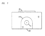
- the waveguide 5 it is alternatively possible for the waveguide 5 to be coupled by the solder within a cavity of such substrate as shown in FIG. 7.
- Similar components of FIGS. 3 and 7 are like numbered for clarity, including the optical fiber 5, substrate 10, and solder 15.
- the optical fiber 5 is positioned within a cavity 310 of the substrate 10.
- the solder composition 15 couples the fiber 5 to the substrate 10 to provide the advantageous acoustic path.
- the solder 15 has an exposed surface 320 having an optional substantially flat shape that advantageously provides reflection of acoustic waves generated by the transducer 20 that are not directly propagated into the optical fiber 5. At least a portion of the acoustic waves that are reflected by such surface 320 propagate into the fiber 5 increasing the acoustic wave energy entering the optical fiber 5 in a similar manner to that previously described with regard to FIG. 6.
- the optical fiber can extend through a hole in the substrate with an acoustically-compatible solder being used to couple the fiber to internal substrate surfaces defining the hole.
- FIGS. 2, 3 and 5-7 depict exemplary embodiments of the invention having the transducer 20 formed on a substantially flat substrate surface for illustration purposes only. It is also possible for the transducer to be formed on substrate surfaces having different shapes, such as having a substantially curved cross-sectional shape to direct generated acoustic waves at a soldered optical waveguide.
- solder compositions for coupling the SiO 2 and LiNbO 3 as the materials for the substrate and optical waveguide
- other materials and acoustically-compatible solder compositions are useable in accordance with the invention as long as such materials have ⁇ •v products relative to one another that achieve a desired propagation efficiency of acoustic waves into the waveguide for modulating signals transmitted therein.
Landscapes
- Physics & Mathematics (AREA)
- Nonlinear Science (AREA)
- General Physics & Mathematics (AREA)
- Optics & Photonics (AREA)
- Optical Modulation, Optical Deflection, Nonlinear Optics, Optical Demodulation, Optical Logic Elements (AREA)
- Optical Couplings Of Light Guides (AREA)
Claims (11)
- Dispositif acousto-optique comprenant :un substrat (10) sur lequel est formé un transducteur (20) ;un guide d'onde optique (5, 7) ; etune composition de brasage acoustiquement compatible (15) couplant ledit guide d'onde (5, 7) audit substrat (10), ladite composition de brasage (15) ayant une densité ρ et une propriété physique permettant à une onde acoustique de se propager à l'intérieur de ladite composition à une vélocité υ, dans lequel un produit densité-vélocité d'onde acoustique ρ·υ de la composition a une valeur relative à des produits densité-vélocité d'onde acoustique correspondants du substrat (10) et du guide d'onde en vue de permettre la propagation d'une onde acoustique générée par ledit transducteur (20) à travers lesdits substrat et composition de brasage dans ledit guide d'onde pour moduler un signal lumineux se propageant à travers ledit guide d'onde,dans lequel ladite composition de brasage acoustiquement compatible (15) couvre une partie suffisante dudit guide d'onde optique (5, 7) en vue de fournir un trajet de brasage entre ledit substrat et ledit guide d'onde optique pour l'entrée des ondes acoustiques dans ledit guide d'onde optique, etdans lequel ladite composition de brasage acoustiquement compatible (15) encapsule ledit guide d'onde optique (5, 7) de telle manière que les ondes acoustiques soient reflétées par la surface de ladite composition de brasage acoustiquement compatible en retour vers ledit guide d'onde optique.
- Dispositif selon la revendication 1, dans lequel ledit produit densité-vélocité d'onde acoustique ρ?ν de ladite composition de brasage diffère par pas plus de 30% desdits produits densité-vélocité d'onde acoustique dudit substrat ou dudit guide d'onde.
- Dispositif selon la revendication 1 ou la revendication 2, dans lequel ladite composition de brasage comprend de l'indium.
- Dispositif selon la revendication 3, dans lequel ladite composition de brasage est au moins de 90% d'indium en poids.
- Dispositif selon l'une quelconque des revendications précédentes, dans lequel ledit substrat est un substrat en SiO2.
- Dispositif selon l'une quelconque des revendications 1 à 4, dans lequel ledit substrat est un substrat en LiNbO3.
- Dispositif selon l'une quelconque des revendications précédentes, dans lequel ledit guide d'onde optique est une fibre optique en SiO2.
- Dispositif selon l'une quelconque des revendications précédentes, dans lequel ladite composition de brasage a une forme superficielle qui reflète et concentre substantiellement au moins une partie d'une onde acoustique générée par ledit transducteur au niveau dudit guide d'onde optique.
- Dispositif selon l'une quelconque des revendications précédentes, dans lequel ladite composition de brasage couple ledit guide d'onde à une surface extérieure dudit substrat.
- Dispositif selon l'une quelconque des revendications 1 à 8, dans lequel ladite composition de brasage couple au moins une section dudit guide d'onde audit substrat à l'intérieur d'une cavité dudit substrat.
- Dispositif selon l'une quelconque des revendications 1 à 8, dans lequel ledit guide d'onde s'étend à travers ledit substrat et ladite composition de brasage couple ledit guide d'onde à une surface interne dudit substrat.
Applications Claiming Priority (2)
| Application Number | Priority Date | Filing Date | Title |
|---|---|---|---|
| US08/798,397 US5757987A (en) | 1997-02-07 | 1997-02-07 | Acousto-optic modulator for optical waveguides |
| US798397 | 1997-02-07 |
Publications (2)
| Publication Number | Publication Date |
|---|---|
| EP0859264A1 EP0859264A1 (fr) | 1998-08-19 |
| EP0859264B1 true EP0859264B1 (fr) | 1999-09-15 |
Family
ID=25173298
Family Applications (1)
| Application Number | Title | Priority Date | Filing Date |
|---|---|---|---|
| EP98300559A Expired - Lifetime EP0859264B1 (fr) | 1997-02-07 | 1998-01-27 | Modulateur acousto-optique comprenant un guide d'onde optique |
Country Status (4)
| Country | Link |
|---|---|
| US (1) | US5757987A (fr) |
| EP (1) | EP0859264B1 (fr) |
| JP (1) | JPH10228008A (fr) |
| DE (1) | DE69800021T2 (fr) |
Cited By (1)
| Publication number | Priority date | Publication date | Assignee | Title |
|---|---|---|---|---|
| US11960156B2 (en) * | 2018-09-18 | 2024-04-16 | Eagle Technology, Llc | Multi-channel laser system including an acousto-optic modulator (AOM) with beam polarization switching and related methods |
Families Citing this family (6)
| Publication number | Priority date | Publication date | Assignee | Title |
|---|---|---|---|---|
| DE19945729B4 (de) * | 1999-09-23 | 2008-04-24 | Jenoptik Ldt Gmbh | Akustooptischer Fasermodulator |
| US6567604B1 (en) * | 2000-10-25 | 2003-05-20 | Omm, Inc. | Indium plated package for an optical component and process therefore |
| US7359523B2 (en) * | 2003-06-17 | 2008-04-15 | Avago Technologies Fiber Ip Pte Ltd | Fluidic acoustic transducer |
| CN109307506A (zh) * | 2017-07-26 | 2019-02-05 | 中国科学院声学研究所 | 一种基于多模式光纤结构的微光机电陀螺 |
| US11307433B2 (en) * | 2020-02-21 | 2022-04-19 | Robotic Research Opco, Llc | Acoustically adjustable lenses |
| CN116149089A (zh) * | 2023-03-01 | 2023-05-23 | 中国科学技术大学 | 声光调制器及其制备方法 |
Family Cites Families (8)
| Publication number | Priority date | Publication date | Assignee | Title |
|---|---|---|---|---|
| US3653743A (en) * | 1970-11-23 | 1972-04-04 | Hughes Aircraft Co | Electro-optic devices with acousto-optic effect suppression |
| JPS51115794A (en) * | 1975-04-02 | 1976-10-12 | Mitsubishi Electric Corp | Thin film photo switch element |
| US4735485A (en) * | 1984-02-17 | 1988-04-05 | The Board Of Trustees Of The Leland Stanford Junior University | Acousto-optic frequency shifter using optical fiber and method of manufacturing same |
| US4735476A (en) * | 1985-09-18 | 1988-04-05 | Board Of Trustees Of The Leland Stanford Junior University | Acousto-optic bragg cell |
| JPH0781911B2 (ja) * | 1987-07-20 | 1995-09-06 | 富士写真フイルム株式会社 | 光スペクトラムアナライザ− |
| US4991923A (en) * | 1989-01-17 | 1991-02-12 | Board Of Trustees Of The Leland Stanford Junior University | Acousto-optic modulator for optical fibers using Hertzian contact with a grooved transducer substrate |
| CA2112480A1 (fr) * | 1992-04-28 | 1993-11-11 | Toshiya Hikami | Modulateur externe pour communication par fibre optique |
| US5351318A (en) * | 1993-04-05 | 1994-09-27 | The Board Of Trustees Of The Leland Stanford Jr./University | Fiber optic communication system and fiber optic modulator |
-
1997
- 1997-02-07 US US08/798,397 patent/US5757987A/en not_active Expired - Lifetime
-
1998
- 1998-01-21 JP JP10009641A patent/JPH10228008A/ja active Pending
- 1998-01-27 DE DE69800021T patent/DE69800021T2/de not_active Expired - Lifetime
- 1998-01-27 EP EP98300559A patent/EP0859264B1/fr not_active Expired - Lifetime
Cited By (1)
| Publication number | Priority date | Publication date | Assignee | Title |
|---|---|---|---|---|
| US11960156B2 (en) * | 2018-09-18 | 2024-04-16 | Eagle Technology, Llc | Multi-channel laser system including an acousto-optic modulator (AOM) with beam polarization switching and related methods |
Also Published As
| Publication number | Publication date |
|---|---|
| JPH10228008A (ja) | 1998-08-25 |
| EP0859264A1 (fr) | 1998-08-19 |
| DE69800021T2 (de) | 2000-04-20 |
| DE69800021D1 (de) | 1999-10-21 |
| US5757987A (en) | 1998-05-26 |
Similar Documents
| Publication | Publication Date | Title |
|---|---|---|
| US7068863B2 (en) | Optical waveguide device, an optical modulator, a mounting structure for an optical waveguide device and a supporting member for an optical waveguide substrate | |
| US5005932A (en) | Electro-optic modulator | |
| US5471545A (en) | Optical external modulator for optical telecommunications | |
| US3856378A (en) | Method and means for modulating light propagating in an optical waveguide by bulk acoustic waves | |
| EP1109054B1 (fr) | Modulateur optique à ondes progressives et son procédé de fabrication | |
| EP0877284B1 (fr) | Commutateur acousto-optique pour circuit optique en silice | |
| US6033126A (en) | Optical waveguide module having improved high-frequency characteristics | |
| US5757987A (en) | Acousto-optic modulator for optical waveguides | |
| US7397974B2 (en) | Optical modulator | |
| US5841913A (en) | Acousto-optic planar waveguide modulators | |
| EP4113181B1 (fr) | Circuit intégré photonique à large bande passante avec compensation de l'étalon | |
| JP2004341147A (ja) | 光導波路デバイスおよび進行波形光変調器 | |
| CA2112480A1 (fr) | Modulateur externe pour communication par fibre optique | |
| JPH02214828A (ja) | 集積化光導波路デバイス | |
| JPH03269505A (ja) | 光フアイバコネクタ | |
| US4707060A (en) | Broadband infrared electro-optic modulator having a buried microstrip network | |
| JP2006246509A (ja) | 高周波線路の接続構造 | |
| JP3824265B2 (ja) | 高周波線路の接続構造 | |
| WO2024201728A1 (fr) | Élément de guide d'ondes optique et dispositif de modulation optique l'utilisant, et dispositif de transmission optique | |
| JPS6344208B2 (fr) | ||
| JPH06230332A (ja) | 外部光変調器 | |
| JPS6298306A (ja) | 波長選択結合器 | |
| JPS63218909A (ja) | 光信号伝送装置 | |
| JPH04349405A (ja) | 光結合回路 | |
| JP2006285290A (ja) | 光導波路モジュール |
Legal Events
| Date | Code | Title | Description |
|---|---|---|---|
| PUAI | Public reference made under article 153(3) epc to a published international application that has entered the european phase |
Free format text: ORIGINAL CODE: 0009012 |
|
| 17P | Request for examination filed |
Effective date: 19980205 |
|
| AK | Designated contracting states |
Kind code of ref document: A1 Designated state(s): DE FR GB NL |
|
| AX | Request for extension of the european patent |
Free format text: AL;LT;LV;MK;RO;SI |
|
| GRAG | Despatch of communication of intention to grant |
Free format text: ORIGINAL CODE: EPIDOS AGRA |
|
| GRAG | Despatch of communication of intention to grant |
Free format text: ORIGINAL CODE: EPIDOS AGRA |
|
| GRAH | Despatch of communication of intention to grant a patent |
Free format text: ORIGINAL CODE: EPIDOS IGRA |
|
| AKX | Designation fees paid |
Free format text: DE FR GB NL |
|
| RBV | Designated contracting states (corrected) |
Designated state(s): DE FR GB NL |
|
| GRAH | Despatch of communication of intention to grant a patent |
Free format text: ORIGINAL CODE: EPIDOS IGRA |
|
| GRAA | (expected) grant |
Free format text: ORIGINAL CODE: 0009210 |
|
| AK | Designated contracting states |
Kind code of ref document: B1 Designated state(s): DE FR GB NL |
|
| REF | Corresponds to: |
Ref document number: 69800021 Country of ref document: DE Date of ref document: 19991021 |
|
| ET | Fr: translation filed | ||
| PLBE | No opposition filed within time limit |
Free format text: ORIGINAL CODE: 0009261 |
|
| STAA | Information on the status of an ep patent application or granted ep patent |
Free format text: STATUS: NO OPPOSITION FILED WITHIN TIME LIMIT |
|
| 26N | No opposition filed | ||
| PGFP | Annual fee paid to national office [announced via postgrant information from national office to epo] |
Ref country code: NL Payment date: 20010109 Year of fee payment: 6 |
|
| REG | Reference to a national code |
Ref country code: GB Ref legal event code: IF02 |
|
| PG25 | Lapsed in a contracting state [announced via postgrant information from national office to epo] |
Ref country code: NL Free format text: LAPSE BECAUSE OF NON-PAYMENT OF DUE FEES Effective date: 20040801 |
|
| NLV4 | Nl: lapsed or anulled due to non-payment of the annual fee |
Effective date: 20040801 |
|
| PGFP | Annual fee paid to national office [announced via postgrant information from national office to epo] |
Ref country code: DE Payment date: 20140122 Year of fee payment: 17 |
|
| PGFP | Annual fee paid to national office [announced via postgrant information from national office to epo] |
Ref country code: FR Payment date: 20140108 Year of fee payment: 17 |
|
| PGFP | Annual fee paid to national office [announced via postgrant information from national office to epo] |
Ref country code: GB Payment date: 20140122 Year of fee payment: 17 |
|
| REG | Reference to a national code |
Ref country code: DE Ref legal event code: R119 Ref document number: 69800021 Country of ref document: DE |
|
| GBPC | Gb: european patent ceased through non-payment of renewal fee |
Effective date: 20150127 |
|
| PG25 | Lapsed in a contracting state [announced via postgrant information from national office to epo] |
Ref country code: DE Free format text: LAPSE BECAUSE OF NON-PAYMENT OF DUE FEES Effective date: 20150801 Ref country code: GB Free format text: LAPSE BECAUSE OF NON-PAYMENT OF DUE FEES Effective date: 20150127 |
|
| REG | Reference to a national code |
Ref country code: FR Ref legal event code: ST Effective date: 20150930 |
|
| PG25 | Lapsed in a contracting state [announced via postgrant information from national office to epo] |
Ref country code: FR Free format text: LAPSE BECAUSE OF NON-PAYMENT OF DUE FEES Effective date: 20150202 |