EP0859524B1 - Decodeur d'images et memoire d'images apportant une reponse aux divers facteurs de retard dus a certaines caracteristiques de materiels propres a la memoire d'images grace a un systeme de stockage et a un systeme de lecture ameliores - Google Patents
Decodeur d'images et memoire d'images apportant une reponse aux divers facteurs de retard dus a certaines caracteristiques de materiels propres a la memoire d'images grace a un systeme de stockage et a un systeme de lecture ameliores Download PDFInfo
- Publication number
- EP0859524B1 EP0859524B1 EP97937819A EP97937819A EP0859524B1 EP 0859524 B1 EP0859524 B1 EP 0859524B1 EP 97937819 A EP97937819 A EP 97937819A EP 97937819 A EP97937819 A EP 97937819A EP 0859524 B1 EP0859524 B1 EP 0859524B1
- Authority
- EP
- European Patent Office
- Prior art keywords
- read
- block
- page
- components
- luminance
- Prior art date
- Legal status (The legal status is an assumption and is not a legal conclusion. Google has not performed a legal analysis and makes no representation as to the accuracy of the status listed.)
- Expired - Lifetime
Links
Images


Classifications
-
- H—ELECTRICITY
- H04—ELECTRIC COMMUNICATION TECHNIQUE
- H04N—PICTORIAL COMMUNICATION, e.g. TELEVISION
- H04N5/00—Details of television systems
- H04N5/76—Television signal recording
- H04N5/907—Television signal recording using static stores, e.g. storage tubes or semiconductor memories
-
- H—ELECTRICITY
- H04—ELECTRIC COMMUNICATION TECHNIQUE
- H04N—PICTORIAL COMMUNICATION, e.g. TELEVISION
- H04N11/00—Colour television systems
- H04N11/04—Colour television systems using pulse code modulation
-
- H—ELECTRICITY
- H04—ELECTRIC COMMUNICATION TECHNIQUE
- H04N—PICTORIAL COMMUNICATION, e.g. TELEVISION
- H04N19/00—Methods or arrangements for coding, decoding, compressing or decompressing digital video signals
- H04N19/42—Methods or arrangements for coding, decoding, compressing or decompressing digital video signals characterised by implementation details or hardware specially adapted for video compression or decompression, e.g. dedicated software implementation
- H04N19/423—Methods or arrangements for coding, decoding, compressing or decompressing digital video signals characterised by implementation details or hardware specially adapted for video compression or decompression, e.g. dedicated software implementation characterised by memory arrangements
-
- H—ELECTRICITY
- H04—ELECTRIC COMMUNICATION TECHNIQUE
- H04N—PICTORIAL COMMUNICATION, e.g. TELEVISION
- H04N19/00—Methods or arrangements for coding, decoding, compressing or decompressing digital video signals
- H04N19/60—Methods or arrangements for coding, decoding, compressing or decompressing digital video signals using transform coding
- H04N19/61—Methods or arrangements for coding, decoding, compressing or decompressing digital video signals using transform coding in combination with predictive coding
Definitions
- the images to be displayed are produced by combining images used as a reference for differential calculation (hereinafter, “reference pictures”) with coded images (hereinafter, “differential pictures”) for calculated differences between images.
- the motion compensation referred to here means the addition (blending) of the appropriate differences to the reference pictures displayed before or after the present frame to form one frame that is a display image.
- DRAM Dynamic Random Access Memory
- SDRAM Synchronous Dynamic Random Access Memory
- a number of luminance components which is equal to the number set as the read length is outputted from the data pins of the SDRAM 226.
- the read length is set as four words, then luminance components for four pixels will be outputted from the data pins.
- the reason the luminance components and chrominance components are stored on different pages in the SDRAM 226 is because these components will be read using burst reads.
- Half-pel interpolation in the vertical axis refers to the generation of components for each line in a luminance block using an average value of a component on a given row and the component on the next row
- half-pel interpolation in the horizontal axis refers to the generation of components for each column in a luminance block using an average value of the component in a given column and the component in the next column
- Half-pel interpolation in the vertical and horizontal directions refers to the generation of components for each column in a luminance block using an average value of a component in a given column, the component in the next column, the component on the next row and the component on the next row and next column.
- the storage areas in the SDRAM that are in matrix form are called memory arrays.
- a plurality of memory arrays are provided in the SDRAM, with such arrays having a large storage capacity. If a plurality of memory arrays are provided, bank addresses will be separately mapped to each of the memory arrays, with it being possible to divide images and store them across a plurality of memory arrays.
- the first object of the present invention which is set out in the claims, is to provide an image decoding apparatus that enables motion compensation to be performed using a low-speed operation clock by reducing the number of reads and read times for reads of luminance components and chrominance components performed on an SDRAM.
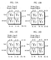
- the dif_Y0 block to dif_Y3 block referred to here are obtained by dividing a block of 16 vertical components by 16 horizontal components into four blocks of 8 horizontal components by 8 vertical components. Once a luminance block composed of 16 horizontal pixels by 16 vertical pixels has been equally divided into four, the dif_Y0 block, dif_Y1 block, dif_Y2 block, and dif_Y3 block are produced as shown in Fig. 13A.
- "dif_" means difference.
- the word length register 59 stores the word length which is to be used for a burst read, and gives an indication to the page data buffer 57 and the page data buffer 58 to output only the data of this word length. It should be noted here that in the first embodiment, the word length of the SDRAM 31 is one byte, and that the luminance component, blue chrominance component, and red chrominance component for one pixel are each expressed using one byte.
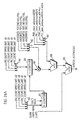
- the compensation control unit 10 determines what areas should be cut out from which coordinates in the images stored in the SDRAM 31 to SDRAM 33 in accordance with the motion vectors outputted by the processor 5.
- the reference coordinates for the cut out are set as (X,Y) and the cut out area is set as m pixels wide by n pixels high.
- the memory access unit 11 performs memory access to read one of the reference pictures in the SDRAM 31 to SDRAM 33. Different amounts of luminance components and the chrominance components of the reference picture can be read, although in the present embodiment a read operation is performed three times for each reference picture.
- the reason that the luminance block is read by performing separate reads for the Y01 block and the Y23 block is so that one extra row and one extra column of luminance components can be written into a buffer whose capacity is 16 horizontal pixels by 16 vertical pixels. This is to say, when the capacity of the buffer is 16 horizontal pixels by 16 vertical pixels and luminance components for 16 horizontal pixels by 16 vertical pixels are written in together, the buffer will be unable to store the extra luminance components, although when the luminance components are written into a buffer with a capacity of 16 horizontal pixels by 16 vertical pixels in two stages, there will be sufficient capacity in the buffer for storing the extra luminance components.
- the reason the reference picture is read using this Y02 block, Y13 block pattern is that the Y02 block, Y13 block pattern is obtained as the result of the IDCT by the pixel calculation unit 7.
- the memory access unit 11 determines a combination of the Cb block and the Cr block (hereinafter, referred to as the "CbCr block”) as the block m pixels wide by n pixels high which is to be read.
- the processor 5 When the outputted differential picture is a B picture, the processor 5 recognizes that this should be added not only to a previous reference picture, but also to a following reference picture, and so the processor 5 also has the following ref_Y01_f(r) block (here, the "f” in “f(r)” means “forward"), the ref_Y23_f(r) block, and the ref_CbCr_f(r) block read from the SDRAM 32 in the memory module 3.
- step S0 the memory access unit 11 sets the Width_Flag and the Height_Flag to "0".
- step S1 the compensation control unit 10 refers to the motion vectors and judges whether half-pel interpolation is necessary in the vertical direction. If so, the compensation control unit 10 sets the Height_Flag at "1" in step S2.
- step S3 the compensation control unit 10 judges whether half-pel interpolation is necessary in the horizontal direction. If so, the compensation control unit 10 sets the Width_Flag at "1" is step S4.
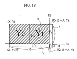
- step S14 a value (width m+1) is added to the X coordinate of the top left vertex of the reference picture.
- the size of this (8,16) block is the same as the size of the Y13 block shown in Fig. 14A with the vertices (8,0), (15,0), (8,15), and (15,15).
- the memory access unit 11 reads an area of the stipulated height and width starting from the indicated top left vertex in the buffer A 12.
- Buffer C 20 stores the results of the half-pel interpolation by the half-pel interpolation unit 15 performs that are outputted in a 16 horizontal pixel by 8 vertical pixel block or a 8 horizontal pixel by 16 vertical pixel block. After the differences that are to be blended with these half-pel interpolation results have been outputted by the buffer D 25, the buffer C 20 outputs the half-pel interpolation results which it has stored so far to the blend unit 29 so that these results can be blended with the differences.
- the chrominance address encoder 62 has an adder 65 and a multiplier 66.
- the adder 65 adds the lower 5 bits of the 8 bits which compose the Y coordinate to the entry column address of the page and generates the upper-order five bits of the column address as the addition result.
- the luminance address encoder 61 encodes the lower-order 4 bits of the coordinate value (X+15-A) as the lower-order 4 bits of the column address and encodes the lower-order 5 bits of the Y coordinate as the higher-order 5 bits of the column address to generate the column address. Meanwhile, the higher-order 6 bits of this coordinate value (X+15-A) are added to the multiplication result of the multiplier 63 to generate the bank address and row address.
- (A+m-15) addresses are read in accordance with the read length of (A+m-15) pixels, and after this read has been performed, the read position has to be moved down by one row.
- the starting coordinates are set at (X,Y+n), and the luminance address encoder 61 converts these coordinates to a row address and column address.
- the luminance address encoder 61 encodes the lower-order 4 bits of the coordinate value X as the lower-order 4 bits of the column address and encodes the lower-order 5 bits of the Y+n coordinate as the higher-order 5 bits of the column address to generate the column address. Meanwhile, the higher-order 6 bits of this coordinate value X are added to the multiplication result of the multiplier 63 to generate the bank address and row address.
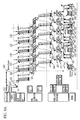
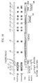
- the "Command” line in Fig. 19 shows the indication of operations to the SDRAM, and as examples, "A1” shows an activation ("A” representing "Activate) of bank 1, "R0” shows a read (“R” representing "Read”) of bank 0, "P1” shows a precharging ("P” representing "Precharge”) of bank 1, and "BS” showing a termination of consecutive transfers (“BS” representing "Burst Stop”).
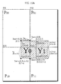
- Step S59 the top left vertex (X,Y) of the Y01 block is positioned towards the top of the 16 horizontal pixels by 32 vertical pixels included in the top left page P00, so that the overlapping parts of the top left page P00 and the top right page P01 have the greatest heights.
- step S68 in Fig. 16 an RAS signal is issued to the RAS pins of the SDRAM at timing c1 and at the same time an activate command for bank 1 of the SDRAM to be read is issued.
- the activate command A1 the activation of bank 1 is performed during the period d1 (the timing d1 mentioned here including the effective activation of the memory array and the CAS delay (labeled as the "CAS latency" in Fig. 19)).
- the timing d1 mentioned here including the effective activation of the memory array and the CAS delay (labeled as the "CAS latency" in Fig. 19)).
- Three clock pulses later at timing c2 an RAS signal is issued to the RAS pins of the SDRAM and at the same time an activate command A0 for bank 0 of the SDRAM is issued.
- the activate command A0 the activation of bank 0 can be performed during the period d2.
- step S24 the column address which has been converted from the relative coordinates (X+15-A,Y+n-31) in the pixel block is outputted to the address pins, and in step S25 the CAS is outputted to the bank address calculated by the luminance address encoder 61 at timing c16 in Fig. 18.
- step S26 the read length "1" is set in the word length register 59 and the read command R0 is issued.
- the buffer A 12 When the luminance components and chrominance components that compose the Y01 block, the Y23 block, and the CbCr block in a future direction are read from the memory access unit 11, the buffer A 12 writes these into one of its internal memory areas in accordance with the write address coordinates indicated by the write address generation unit 13. The buffer A 12 also outputs data at the read address coordinates indicated by the read address generation unit 14, out of the luminance components and chrominance components written into the internal memory areas, to the half-pel interpolation unit 15.
- the write address generation unit 13 When the compensation control unit 10 has started to read the luminance components and the chrominance components from the SDRAM, the write address generation unit 13 generates a linear address and has the read luminance components and chrominance components written into the buffer A 12 at the area indicated by the generated linear address.
- the selector 85 When the read pattern is set for the Y02 block and half-pel interpolation in the horizontal direction is necessary, luminance components are read in a block of 9 horizontal pixels by 16 vertical pixels. Since luminance components are stored for nine pixels, the selector 85 outputs the value "+3" to the multiplier 86. By outputting the value "+3" to the multiplier 86 in this way, the increase in the count value can be tripled every time the Y counter 83 increments the Y coordinate.
- the start address for storing an overlapping part read from the top left page P00 may be set as the address 0000 in the buffer A 12, so that in this case the selector 87 can output the linear address 0000 to the adder 88.
- Y01(14,8), Y01(15,8), Y01(16,8) are not overwritten and so remain in the buffer A 12.
- the reason this one row of luminance components is allowed to remain in the buffer A 12 is that of the pixels in the Y23 block, the luminance components of the pixels with the row addresses Y23(0,0), Y23(1,0), Y23(2,0), Y23(3,0), ... Y23(14,0), Y23(15,0), Y23(16,0) are generated by taking an average with the luminance components on this ninth row.
- Fig. 26A the internal area of the buffer A 12 completely used up by the 9 horizontal pixels by 17 vertical pixels included in the Y02 block, but when the Y13 block is read, the 8 horizontal pixels by 17 vertical pixels included in the Y13 block are overwritten into the internal area of the buffer A 12 that is used for the Y02 block in Fig. 26A.
- the Y02 block is composed of 9 horizontal pixels by 17 vertical pixels and includes one more column of luminance components than the Y13 block, the luminance components in the ninth column Y02(8,0), Y02(8,1), Y02(8,2), Y02(8,3), ...
- Y02(8,14), Y02(8,15), Y02(8,16) are not overwritten and so remain in the buffer A 12.
- the reason this one column of luminance components is allowed to remain in the buffer A 12 is that of the pixels in the Y13 block, the luminance components of the pixels with the column addresses Y13(0,0), Y13(0,1), Y13(0,2), Y13(0,3) ... Y13(0,14), Y13(0,15), Y13(0,16) are generated by taking an average with the luminance components in this ninth column.
- the MOD calculator 93 adds "1" to the count value outputted by the X counter 91 as the X coordinate and outputs the remainder of the addition result divided by the total number of columns z to the buffer A 12.
- the divider 103 divides the addition result of the adder 102 by two. When half-pel interpolation is not required in either of the horizontal or vertical directions, the value which was outputted through the divider 96 is again outputted without amendment.
- the read address generation unit 18 has the same configuration as the read address generation unit 14 and outputs the X coordinate and Y coordinate of the read address coordinates that should be blended with the differences and outputs the generated coordinates to the buffer B 16.
- the adder 76 adds the result of the multiplier 74 having multiplied the count value of the X counter 71 by "2" to the first coordinate outputted by the selector 75.
- the selector 79 outputs a first coordinate of a read address or a write address to the adder 80.
- the selector 79 When half-pel interpolation is performed for the Y01 block, the Y23 block, the Y02 block, the Y13 block, or the CbCr block and the next difference to be blended is for the Y0 block, the Y1 block, the Y2 block, the Y3 block, the Cb block, or the Cr block, the selector 79 outputs "0" to the adder 80 as the first Y coordinate for the read address and write address.
- the X counter 27 and the Y counter 28 output the same values to the buffer D 25 as the write address for calculation result of the half-pel interpolation unit 15, and the result of the addition by the blend unit 29 is stored in the buffer C 20 as the luminance component for the same coordinates.
- the luminance components Y01(4,0), Y01(5,0), Y01(4,1), and Y01(5,1) are outputted from the buffer A 12 and an average of these values is calculated by the half-pel interpolation unit 15.
- the luminance components Y01(13,8), Y01(14,8), Y23(13,0), and Y23(14,0) are outputted from the buffer A 12 and an average of these values is calculated by the half-pel interpolation unit 15.
- the X counter 27 and the Y counter 28 output the same values to the buffer D 25 as the write address for calculation result of the half-pel interpolation unit 15, and the result of the addition by the blend unit 29 is stored in the buffer C 20 as the luminance component for the same coordinates.
- the luminance components Y01(15,8), Y01(16,8), Y23(15,0), and Y23(16,0) are outputted from the buffer A 12 and an average of these values is calculated by the half-pel interpolation unit 15.
- the X counter 27 and the Y counter 28 output the same values to the buffer D 25 as the write address for calculation result of the half-pel interpolation unit 15, and the result of the addition by the blend unit 29 is stored in the buffer C 20 as the luminance component for the same coordinates.
- the luminance components Y23(13,6). Y23(14,6), Y23(13,7), and Y23(14,7) are outputted from the buffer A 12 and an average of these values is calculated by the half-pel interpolation unit 15.
- the luminance components included in the Y02 block are calculated using the average values of the luminance components themselves, the luminance component positioned to the right, the luminance component below, and the luminance component below and to the right.
- the luminance components included in the Y13 block are generated using the average values of the luminance components themselves, the luminance component to the left, the luminance component directly below, and the luminance component below and to the left.
- the buffer D 25 stores this block at timing g1.
- the Y02 block of the reference picture is read and at timing g3 half-pel interpolation is performed on the read Y02 block, with the result of the half-pel interpolation being outputted to the blend unit 29 so that it can be blended with the Y0 block.
- the number of burst reads can be reduced to a number that is proportionate to two reads of the reference picture.
- the influence of the delay tRCD between the issuance of a row address and the issuance of a column address can be remarkably reduced.
- the luminance address encoder 61 and the chrominance address encoder 62 are configured as shown in Figs. 30A and 30B. As shown in Fig. 30A, the luminance address encoder 61 has been amended so that the column address is created using the three bits from the second bit to the fourth bit of the X coordinate.
- the chrominance address encoder 62 has been amended so that the 0 th bit is no longer used to distinguish between blue chrominance components and red chrominance components and that the X coordinate of blue chrominance components and red chrominance components is expressed as the 0 th bit to 3 rd bit.
- the word length of the SDRAM is set at two bytes and the luminance components, blue chrominance components, and red chrominance components are each one byte in length, so that two luminance components or a pair of a blue chrominance component and a red chrominance component can be stored in one word in the SDRAM.
Landscapes
- Engineering & Computer Science (AREA)
- Multimedia (AREA)
- Signal Processing (AREA)
- Compression Or Coding Systems Of Tv Signals (AREA)
- Color Television Systems (AREA)
- Memory System (AREA)
Claims (5)
- Appareil de décodage d'images équipé d'une mémoire d'images,
dans lequel la mémoire d'images (3) comprend des réseaux de mémoires, chaque réseau de mémoires étant une région de stockage en forme de réseau (51, 52) stockant une image en divisant l'image en une pluralité de blocs d'image qui mesurent chacun m pixels de large sur n pixels de haut, où m, n sont des entiers qui sont égaux ou supérieurs à 1,
1a région de stockage en forme de réseau (51, 52) est composée d'une pluralité de régions de pages comprenant une première et une seconde régions de pages,
la première région de page stocke s*t composantes de chrominance rouge et s*t composantes de chrominance bleue, où s, t sont des entiers et sont égaux ou supérieurs à 1, qui appartiennent à un bloc d'image,
la seconde région de page stocke m*n composantes de luminance qui appartiennent au bloc d'image,
la première région de page commence par une zone spécifiée par une adresse de rangée et un première adresse de colonne et se termine par une zone spécifiée par ladite adresse de rangée et une seconde adresse de colonne, et
la seconde région de page commence par une zone spécifiée par une autre adresse de rangée et une troisième adresse de colonne et se termine par une zone spécifiée par ladite autre adresse de rangée et une quatrième adresse de colonne,
l'appareil de décodage d'images comprenant :un moyen de décodage d'images différentielles (6) destiné à décoder un flux transmis depuis l'extérieur afin d'obtenir une image différentielle et des vecteurs de mouvement ;des moyens d'accès à la mémoire (11) destinés à lire des composantes de luminance et des composantes de chrominance à partir des régions de pages dans les réseaux de mémoires ; etun moyen d'ajout (29) destiné à ajouter lesdites composantes, lues à partir de la pluralité de régions de pages, à l'image différentielle,caractérisé en ce que l'appareil de décodage d'images comprend en outre :un moyen de détermination de partie de chevauchement destiné à calculer, lorsqu'une zone de lecture (Y0, Y1) à ajouter à l'image différentielle chevauche une pluralité de régions de pages (P00, P01, P10, P11), les coordonnées de vertex des parties de ladite zone de lecture chevauchant chaque région de page ; etun moyen de détermination d'ordre destiné à déterminer un ordre de lecture desdites parties de chevauchement en comparant respectivement les largeurs horizontales et les hauteurs verticales desdites parties de chevauchement ;dans lequel les moyens d'accès à la mémoire (11) sont agencés afin de lire les composantes de luminance et les composantes de chrominance des parties de chevauchement à partir des régions de pages dans les réseaux de mémoires selon l'ordre de lecture déterminé. - Appareil de décodage d'images selon la revendication 1,
dans lequel, lorsque la zone de lecture chevauche deux régions de pages (P00, P01, P10, P11) qui sont reliées dans la direction horizontale, l'unité de détermination de l'ordre détermine l'ordre de lecture de telle sorte que la partie de chevauchement horizontalement plus large soit lue en premier et que la partie de chevauchement horizontalement plus étroite soit lue ensuite. - Appareil de décodage d'images selon la revendication 2,
dans lequel, lorsque la zone de lecture chevauche quatre régions de pages (P00, P01, P10, P11), l'unité de détermination de l'ordre détermine l'ordre de lecture de telle sorte que la partie de chevauchement horizontalement la plus étroite mais verticalement la plus longue soit lue en premier et qu'une partie de chevauchement horizontalement la plus courte et verticalement la plus courte soit lue en dernier. - Appareil de décodage d'images selon la revendication 3, comprenant en outre :un moyen de transmission de commande de lecture qui, lorsque la zone de lecture a été calculée, transmet une pluralité de commandes de lecture permettant de lire les parties de chevauchement calculées à partir d'une pluralité de régions de pages ;un moyen de transmission de commande de précharge qui transmet une commande de précharge permettant de pré-charger des régions de pages qui stockent les parties de chevauchement restantes après que le moyen de transmission de commande de lecture ait transmis une commande de lecture finale permettant de lire un contenu d'une partie de chevauchement ; etun moyen de transmission de commande d'activation qui transmet une commande d'activation permettant d'activer les régions de pages qui stockent la partie de chevauchement restante après que le moyen de transmission de commande de lecture ait transmis la commande de lecture finale permettant de lire un contenu d'une partie de chevauchement.
- Appareil de décodage d'images selon la revendication 4,
dans lequel, lorsque l'ordre de lecture a été déterminé de telle sorte qu'une zone de lecture ayant une partie de chevauchement horizontalement la plus étroite mais verticalement la plus longue soit la première, le moyen de transmission de commande d'activation transmet une commande d'activation permettant d'activer une pluralité d'adresses de banques avant qu'une commande de lecture ne soit transmise pour la mémoire d'images (3).
Applications Claiming Priority (3)
| Application Number | Priority Date | Filing Date | Title |
|---|---|---|---|
| JP22885096 | 1996-08-29 | ||
| JP228850/96 | 1996-08-29 | ||
| PCT/JP1997/002995 WO1998009444A1 (fr) | 1996-08-29 | 1997-08-28 | Decodeur d'images et memoire d'images apportant une reponse aux divers facteurs de retard dus a certaines caracteristiques de materiels propres a la memoire d'images grace a un systeme de stockage et a un systeme de lecture ameliores |
Publications (3)
| Publication Number | Publication Date |
|---|---|
| EP0859524A1 EP0859524A1 (fr) | 1998-08-19 |
| EP0859524A4 EP0859524A4 (fr) | 2000-11-22 |
| EP0859524B1 true EP0859524B1 (fr) | 2007-06-27 |
Family
ID=16882861
Family Applications (1)
| Application Number | Title | Priority Date | Filing Date |
|---|---|---|---|
| EP97937819A Expired - Lifetime EP0859524B1 (fr) | 1996-08-29 | 1997-08-28 | Decodeur d'images et memoire d'images apportant une reponse aux divers facteurs de retard dus a certaines caracteristiques de materiels propres a la memoire d'images grace a un systeme de stockage et a un systeme de lecture ameliores |
Country Status (7)
| Country | Link |
|---|---|
| US (1) | US6075899A (fr) |
| EP (1) | EP0859524B1 (fr) |
| JP (1) | JP3294854B2 (fr) |
| KR (1) | KR100440522B1 (fr) |
| CN (1) | CN1162010C (fr) |
| DE (1) | DE69737852T2 (fr) |
| WO (1) | WO1998009444A1 (fr) |
Families Citing this family (33)
| Publication number | Priority date | Publication date | Assignee | Title |
|---|---|---|---|---|
| US6104416A (en) * | 1997-11-18 | 2000-08-15 | Stmicroelectronics, Inc. | Tiling in picture memory mapping to minimize memory bandwidth in compression and decompression of data sequences |
| US6028612A (en) * | 1997-11-18 | 2000-02-22 | Stmicroelectronics, Inc. | Picture memory mapping to minimize memory bandwidth in compression and decompression of data sequences |
| EP1645966A1 (fr) * | 1999-10-29 | 2006-04-12 | Sony Corporation | Support de stockage, procédé et dispositif de traitment d'informations |
| US6542541B1 (en) | 2000-01-12 | 2003-04-01 | Sony Corporation | Method and apparatus for decoding MPEG video signals using multiple data transfer units |
| US6944087B2 (en) * | 2001-02-24 | 2005-09-13 | Intel Corporation | Method and apparatus for off boundary memory access |
| EP1185109A1 (fr) * | 2000-08-10 | 2002-03-06 | Siemens Aktiengesellschaft | Procédé et dispositif de stockage d'image vidéo en mémoire et dispositif de radio mobile associé |
| JP4321064B2 (ja) | 2001-03-05 | 2009-08-26 | 株式会社ニコン | 画像処理装置および画像処理プログラム |
| JP4078132B2 (ja) * | 2002-06-28 | 2008-04-23 | キヤノン株式会社 | 画像処理装置及びその方法 |
| JP4078906B2 (ja) * | 2002-07-19 | 2008-04-23 | ソニー株式会社 | 画像信号の処理装置および処理方法、画像表示装置、それに使用される係数データの生成装置および生成方法、並びに各方法を実行するためのプログラムおよびそのプログラムを記録したコンピュータ読み取り可能な媒体 |
| JP4319984B2 (ja) * | 2002-09-02 | 2009-08-26 | セッテック インコーポレイテッド | 記録媒体複製用の複製装置、その方法、及びそのコンピュータプログラム |
| US6925117B2 (en) * | 2003-03-12 | 2005-08-02 | Kabushiki Kaisha Toshiba | Data transmission apparatus, method and program, data reception apparatus and method, and data transmission and reception system, using differential data |
| KR100510677B1 (ko) * | 2003-03-19 | 2005-08-31 | 엘지전자 주식회사 | 메모리 억세스 제어 장치 |
| JP2004336451A (ja) * | 2003-05-08 | 2004-11-25 | Matsushita Electric Ind Co Ltd | 画像復号ユニットとそれを用いた画像符号化装置及び符号化方法並びに画像復号装置及び復号方法 |
| JPWO2005109205A1 (ja) * | 2004-04-15 | 2008-03-21 | 松下電器産業株式会社 | 情報処理装置およびデータアクセス方法 |
| JP4476065B2 (ja) * | 2004-07-29 | 2010-06-09 | 富士通マイクロエレクトロニクス株式会社 | 画像処理システム |
| US7649531B2 (en) * | 2004-09-06 | 2010-01-19 | Panasonic Corporation | Image generation device and image generation method |
| KR100695141B1 (ko) * | 2005-02-15 | 2007-03-14 | 삼성전자주식회사 | 영상처리시스템에 있어서 메모리 억세스장치 및 방법, 데이터 기록장치 및 방법과 데이터 독출장치 및 방법 |
| US20060204125A1 (en) * | 2005-03-09 | 2006-09-14 | Kempf Jeffrey M | Multi-dimensional keystone correction image projection system and method |
| CN103458243B (zh) * | 2005-04-13 | 2017-03-01 | 汤姆逊许可公司 | 视频解码方法和设备 |
| US7660354B2 (en) * | 2005-05-11 | 2010-02-09 | Fang Shi | Temporal error concealment for bi-directionally predicted frames |
| JP4762095B2 (ja) * | 2006-09-20 | 2011-08-31 | 株式会社東芝 | 画像復号装置及び画像復号方法 |
| US20100118943A1 (en) * | 2007-01-09 | 2010-05-13 | Kabushiki Kaisha Toshiba | Method and apparatus for encoding and decoding image |
| US8472066B1 (en) | 2007-01-11 | 2013-06-25 | Marvell International Ltd. | Usage maps in image deposition devices |
| EP2188979A2 (fr) * | 2007-09-10 | 2010-05-26 | Nxp B.V. | Procédé et appareil d'estimation de mouvement dans des données d'images vidéo |
| JP4695124B2 (ja) * | 2007-09-13 | 2011-06-08 | 日本電信電話株式会社 | 動画像符号化における動き探索装置 |
| US8358314B2 (en) * | 2008-02-08 | 2013-01-22 | Apple Inc. | Method for reducing framebuffer memory accesses |
| WO2009136051A2 (fr) * | 2008-04-15 | 2009-11-12 | France Telecom | Codage et decodage d'une image ou d'une sequence d'images decoupees selon des partitions de pixels de forme lineaire |
| US8587598B2 (en) * | 2009-10-29 | 2013-11-19 | Mediatek Inc. | Memory address mapping method for controlling storage of images in memory device and memory address mapping circuit thereof |
| JP5662233B2 (ja) * | 2011-04-15 | 2015-01-28 | 株式会社東芝 | 画像符号化装置及び画像復号装置 |
| JP6084000B2 (ja) * | 2012-10-18 | 2017-02-22 | 株式会社メガチップス | 画像処理装置 |
| FR3009432B1 (fr) | 2013-08-05 | 2016-12-23 | Commissariat Energie Atomique | Circuit integre sur soi muni d'un dispositif de protection contre les decharges electrostatiques |
| US11394987B2 (en) * | 2020-12-11 | 2022-07-19 | Qualcomm Incorporated | Chroma samples from luma samples prediction for video coding |
| CN115426466B (zh) * | 2022-08-22 | 2024-12-31 | 珠海一微半导体股份有限公司 | 一种图像数据的读写控制系统及读写控制方法 |
Family Cites Families (9)
| Publication number | Priority date | Publication date | Assignee | Title |
|---|---|---|---|---|
| CA2062200A1 (fr) * | 1991-03-15 | 1992-09-16 | Stephen C. Purcell | Processeur de decompression pour applications video |
| JPH05244438A (ja) * | 1992-02-28 | 1993-09-21 | Canon Inc | 圧縮伸長回路 |
| TW245871B (en) * | 1994-08-15 | 1995-04-21 | Gen Instrument Corp | Method and apparatus for efficient addressing of dram in a video decompression processor |
| JPH0877345A (ja) * | 1994-09-09 | 1996-03-22 | Toshiba Corp | 画像データ処理装置 |
| DE4441295A1 (de) * | 1994-11-21 | 1996-05-23 | Sican Gmbh | Verfahren und Schaltungsanordnung zur Adressierung von Komponenten blockweise organisierter digitaler Bilddaten in einem Speicher mit Page-Adressierung |
| JP3120010B2 (ja) * | 1994-12-28 | 2000-12-25 | 株式会社グラフィックス・コミュニケーション・ラボラトリーズ | 画像復号処理方法および画像復号装置 |
| JP3624457B2 (ja) * | 1995-04-07 | 2005-03-02 | ソニー株式会社 | 画像信号符号化装置及び画像信号復号化装置 |
| US5960115A (en) * | 1995-07-11 | 1999-09-28 | Xerox Corporation | Method for decompressing multiple codes in a single clock cycle |
| JP3880088B2 (ja) * | 1995-12-28 | 2007-02-14 | キヤノン株式会社 | 符号化装置及び復号化装置 |
-
1997
- 1997-08-28 CN CNB971911444A patent/CN1162010C/zh not_active Expired - Lifetime
- 1997-08-28 DE DE1997637852 patent/DE69737852T2/de not_active Expired - Lifetime
- 1997-08-28 EP EP97937819A patent/EP0859524B1/fr not_active Expired - Lifetime
- 1997-08-28 JP JP50782598A patent/JP3294854B2/ja not_active Expired - Lifetime
- 1997-08-28 WO PCT/JP1997/002995 patent/WO1998009444A1/fr not_active Ceased
- 1997-08-28 KR KR10-1998-0703148A patent/KR100440522B1/ko not_active Expired - Lifetime
- 1997-08-29 US US09/066,308 patent/US6075899A/en not_active Expired - Lifetime
Non-Patent Citations (1)
| Title |
|---|
| None * |
Also Published As
| Publication number | Publication date |
|---|---|
| US6075899A (en) | 2000-06-13 |
| CN1199533A (zh) | 1998-11-18 |
| DE69737852D1 (de) | 2007-08-09 |
| KR19990067196A (ko) | 1999-08-16 |
| KR100440522B1 (ko) | 2004-10-15 |
| EP0859524A1 (fr) | 1998-08-19 |
| CN1162010C (zh) | 2004-08-11 |
| WO1998009444A1 (fr) | 1998-03-05 |
| EP0859524A4 (fr) | 2000-11-22 |
| JP3294854B2 (ja) | 2002-06-24 |
| DE69737852T2 (de) | 2007-10-18 |
Similar Documents
| Publication | Publication Date | Title |
|---|---|---|
| EP0859524B1 (fr) | Decodeur d'images et memoire d'images apportant une reponse aux divers facteurs de retard dus a certaines caracteristiques de materiels propres a la memoire d'images grace a un systeme de stockage et a un systeme de lecture ameliores | |
| JPWO1998009444A1 (ja) | 画像メモリ特有のハードウェアスペックに起因する各種の遅延要因を格納方式及び読出方式の改善により克服した画像復号装置及び画像メモリ | |
| US6996174B2 (en) | MPEG video decoder with integrated scaling and display functions | |
| US6088047A (en) | Motion compensated digital video decoding with buffered picture storage memory map | |
| US5473378A (en) | Motion compensating inter-frame predictive picture coding apparatus | |
| US6088391A (en) | Method and apparatus for segmenting memory to reduce the memory required for bidirectionally predictive-coded frames | |
| US5357282A (en) | Video decoder with parallel implementation | |
| US7773676B2 (en) | Video decoding system with external memory rearranging on a field or frames basis | |
| KR19980019167A (ko) | 블록 지향 이미지 처리 시스템용 이미지 기억 시스템 및 방법(Image storage system and method for a block oriented image processing systems) | |
| US6525783B1 (en) | Video decoding system | |
| WO1999066733A2 (fr) | Systeme de memorisation de donnees de pixel a utiliser dans l'interpolation de demi-pixels | |
| US6020924A (en) | Reduced memory size set top box which stores frames and associated motion vectors which indicate which block or blocks are to be retrieved from memory | |
| EP0714212A2 (fr) | Décodeur vidéo employant traitement concurrent et partage de ressources | |
| EP1147671B1 (fr) | Procede et dispositif pour la compensation du mouvement dans un moteur de mappage de texture | |
| JPH08294115A (ja) | Mpeg復号化器及びその復号化方法 | |
| JPH10178644A (ja) | 動画像復号装置 | |
| US5883679A (en) | Scanning scheme for images stored in dynamic random access memory | |
| GB2311680A (en) | Reordering frames in MPEG coder/decoder | |
| JPH1188886A (ja) | 圧縮動画像信号のデコード装置 | |
| US6307969B1 (en) | Dynamic image encoding method and apparatus | |
| US5467135A (en) | Apparatus and method for moving picture coding | |
| US20030123555A1 (en) | Video decoding system and memory interface apparatus | |
| JPH07298264A (ja) | 画像データの処理方法およびそれに用いる記憶装置ならびに画像データの処理装置 | |
| WO1998044745A1 (fr) | Appareil et procede de decompression video simultanee | |
| JP2002058044A (ja) | 画像復号装置及び画像メモリ |
Legal Events
| Date | Code | Title | Description |
|---|---|---|---|
| PUAI | Public reference made under article 153(3) epc to a published international application that has entered the european phase |
Free format text: ORIGINAL CODE: 0009012 |
|
| 17P | Request for examination filed |
Effective date: 19980501 |
|
| AK | Designated contracting states |
Kind code of ref document: A1 Designated state(s): DE FR GB |
|
| A4 | Supplementary search report drawn up and despatched |
Effective date: 20001006 |
|
| AK | Designated contracting states |
Kind code of ref document: A4 Designated state(s): DE FR GB |
|
| RIC1 | Information provided on ipc code assigned before grant |
Free format text: 7H 04N 11/04 A, 7H 04N 9/808 B, 7H 04N 7/24 B, 7H 04N 7/50 B, 7H 04N 7/36 B |
|
| 17Q | First examination report despatched |
Effective date: 20031014 |
|
| GRAP | Despatch of communication of intention to grant a patent |
Free format text: ORIGINAL CODE: EPIDOSNIGR1 |
|
| GRAS | Grant fee paid |
Free format text: ORIGINAL CODE: EPIDOSNIGR3 |
|
| GRAA | (expected) grant |
Free format text: ORIGINAL CODE: 0009210 |
|
| AK | Designated contracting states |
Kind code of ref document: B1 Designated state(s): DE FR GB |
|
| REG | Reference to a national code |
Ref country code: GB Ref legal event code: FG4D |
|
| REF | Corresponds to: |
Ref document number: 69737852 Country of ref document: DE Date of ref document: 20070809 Kind code of ref document: P |
|
| ET | Fr: translation filed | ||
| PLBE | No opposition filed within time limit |
Free format text: ORIGINAL CODE: 0009261 |
|
| STAA | Information on the status of an ep patent application or granted ep patent |
Free format text: STATUS: NO OPPOSITION FILED WITHIN TIME LIMIT |
|
| 26N | No opposition filed |
Effective date: 20080328 |
|
| REG | Reference to a national code |
Ref country code: FR Ref legal event code: CD Owner name: PANASONIC CORPORATION, JP Effective date: 20150120 |
|
| REG | Reference to a national code |
Ref country code: DE Ref legal event code: R082 Ref document number: 69737852 Country of ref document: DE Representative=s name: GRUENECKER PATENT- UND RECHTSANWAELTE PARTG MB, DE |
|
| REG | Reference to a national code |
Ref country code: DE Ref legal event code: R082 Ref document number: 69737852 Country of ref document: DE Representative=s name: GRUENECKER PATENT- UND RECHTSANWAELTE PARTG MB, DE Effective date: 20150316 Ref country code: DE Ref legal event code: R081 Ref document number: 69737852 Country of ref document: DE Owner name: GODO KAISHA IP BRIDGE 1, JP Free format text: FORMER OWNER: PANASONIC CORPORATION, KADOMA-SHI, OSAKA, JP Effective date: 20150316 |
|
| REG | Reference to a national code |
Ref country code: FR Ref legal event code: TP Owner name: GODO KAISHA IP BRIDGE 1, JP Effective date: 20150422 |
|
| REG | Reference to a national code |
Ref country code: GB Ref legal event code: 732E Free format text: REGISTERED BETWEEN 20150611 AND 20150617 |
|
| REG | Reference to a national code |
Ref country code: FR Ref legal event code: PLFP Year of fee payment: 20 |
|
| PGFP | Annual fee paid to national office [announced via postgrant information from national office to epo] |
Ref country code: GB Payment date: 20160824 Year of fee payment: 20 Ref country code: DE Payment date: 20160823 Year of fee payment: 20 |
|
| PGFP | Annual fee paid to national office [announced via postgrant information from national office to epo] |
Ref country code: FR Payment date: 20160712 Year of fee payment: 20 |
|
| REG | Reference to a national code |
Ref country code: DE Ref legal event code: R071 Ref document number: 69737852 Country of ref document: DE |
|
| REG | Reference to a national code |
Ref country code: GB Ref legal event code: PE20 Expiry date: 20170827 |
|
| PG25 | Lapsed in a contracting state [announced via postgrant information from national office to epo] |
Ref country code: GB Free format text: LAPSE BECAUSE OF EXPIRATION OF PROTECTION Effective date: 20170827 |